Introduction
This is the week I have been looking forward the most. As I wrote previously I've always worked with perfBoard and I've always designed my circuits basically with pen and paper. So this week should have been the one where I was finally leveling up and becoming more efficient and productive for my future electronic projects.
 Some of my circuits hand made design
Unfortunately the beginning was not as I expected, this is the first critic that I want to point out since I started the FabAcademy.
In the past lessons (for example, while explaining 3d printing and modeling concepts, as well the explanation of programmers and FTDI etc) I have always been amazed by the ability of the instructors to summarize everything in essential concepts that would allow us to immediately put our hands on the machines and practice.
Instead during the electronic lesson if I wasn't already super familiar with these concepts I would have lost it, I imagine my classmates how few the have really assimilated during the class.
The only thing I really needed help with was setting up the EDA program, but the instructor in charge of the lesson (who is more specialized in design and 3d printing rather than electronics) couldn't figure out how to fix my problem.
Something I solved the day after and it was due to the version of Kicad 5 (that we were told to use) having conflicts with the FabLab symbols and footprint libraries.
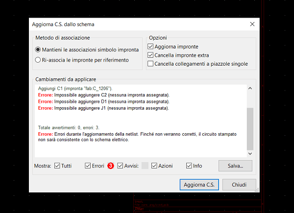 First Errors using KiCad
So unfortunately the start was very disappointing, if I were in charge of the lesson I would have changed how the concepts were presented. But the disappointment didn't last too much anyway, the day after was way better and in the end turned out to be a very productive week.
Bits of the lesson
Before diving into my experience with kicad, I had the lesson with the instructor Oscar. The most remarkable concepts for me are the following:
Workflow
The work flow to produce a custom designed PCB consists of the following steps:
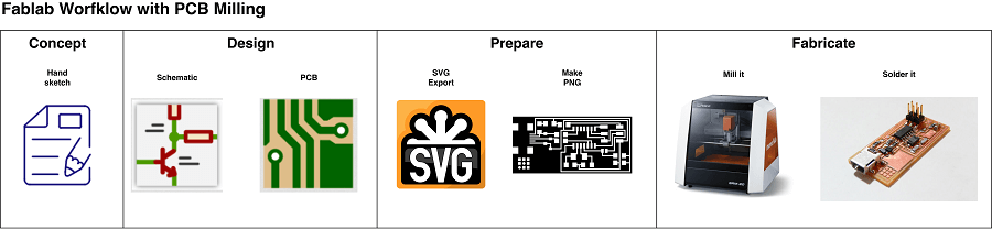 Workflow
I will now describe the steps in detail:
Schematic
This is the part I am already familiar with as I am used to drawing circuit diagrams, mostly on paper and on some simulators.
Basically we proceed by inserting circuit components and connecting them together through wires.
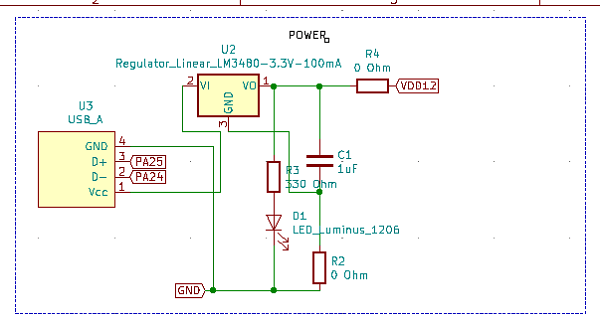 Kicad Circuit DIagram
To speed up the creation of the schematic it is very useful to know the keystrokes:
KiCad Keystrokes
The label function is very useful is which allows you to divide your circuit into many small sub-circuits but still connected to each other, in order to have one easily interpretable electronic scheme.
 Tidy wiring diagram image
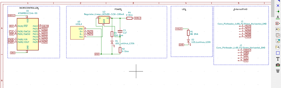
In my case, as a first practice exercise, I built a programmable board with the SAMD11C microcontroller, I added several external pins so that I can modularly connect other boards with different types of sensors without having to rebuild another PCB from scratch.
Other components I have inserted are a LED between USB power rails and another one connected directly to a pin of the microcontroller, then a voltage regulator obviously, with a capacitor and resistors for the LEDs.
You can also see I inserted a USB type-A connector traces, a footprint that is NOT present in the original library of kiCad but I, with the help of my istructor Oscar, created it appositely. Below I described the procedure.
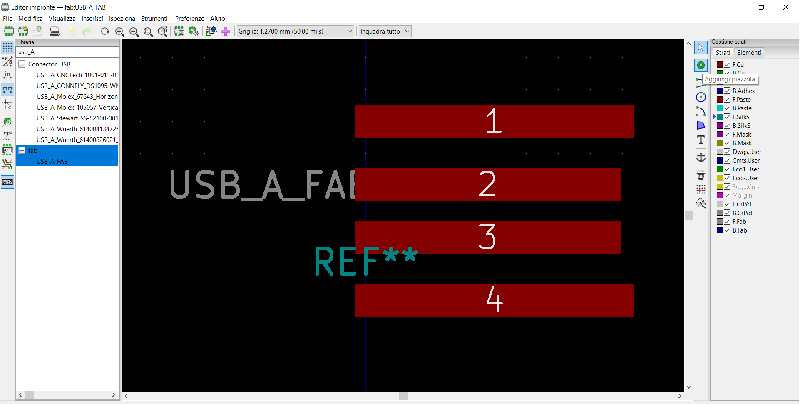 USB connector traces
PCB creation
Once the wiring diagram is done, I proceed by generating the netlist and passing to the PCB creation view, called PCBnew.
Here you can decide the places and the orientation of the components you want to have on your PCB. Once you're satisfied with that, next step is to connect them with
traces (you need to do this only after setting PCB rules, such as the distance of the traces (clearence) that it cannot be less than 0.4 mm, (that because the dimension of the smallest mill-bit we use for the traces is 1/64 = 0.015625 inches that is equal to 0.396875 mm), and also set the traces width of 0.3 mm for adequate electrical conductivity).
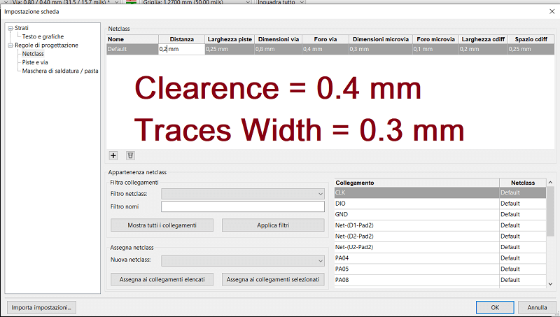 board setting
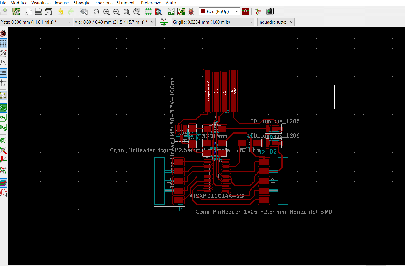
Connecting the traces is a lot of fun at first because it looks like a game. A little less when you spend almost 3 hours there, after several attempts,
forced to go back to modify the schematic and update each time the netlist.
I also had to add 0 ohm resistors to bridge zones of my PCB and to avoid crossing traces. I was about to add FOUR of 'em'! But thanks to my instructor Josep we managed to decrease them by just two.
 PCB traces completed
This is the result after milling the board, unfortunately some traces broke in a couple of points that I promptly fixed with solder and small pieces of wire. In the end everything worked, and I was able to program it as I explain below.
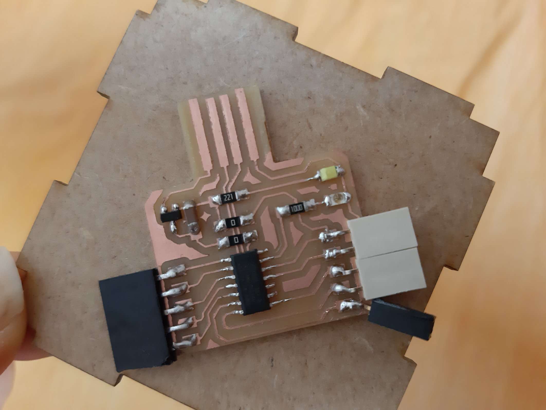 PCB board, stuffed
Programming my new Board
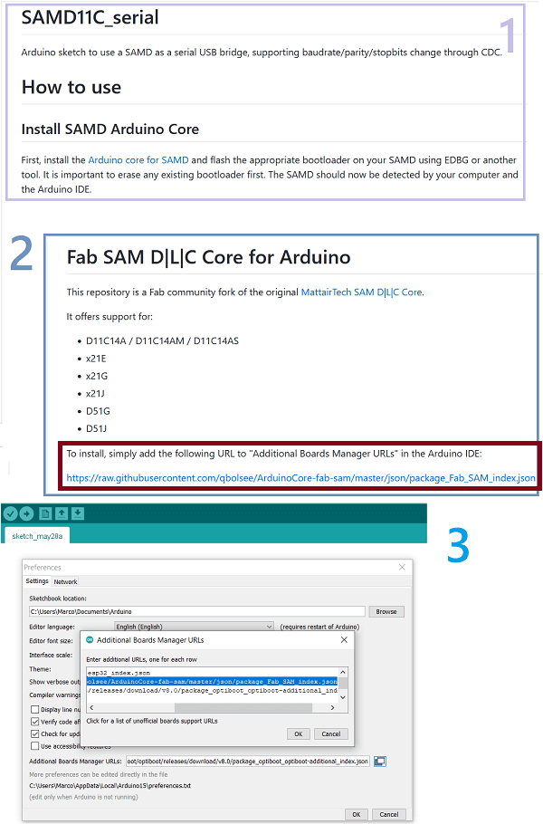
To burn the bootloader into my board and then make it compatible with the arduino IDE I have followed the procedure indicated on this SAMDino WebSite.
 image of the guide website / arduino ide
Basically I first flashed the Serial Interface bootloader into the SAMD11C, then I passed to the Arduino IDE where I installed Arduino core for SAMD (link), in the end I changed some settings as
indicated and here we are! I was able to upload my first Blink program!
 Installing the Arduino core for SAMD
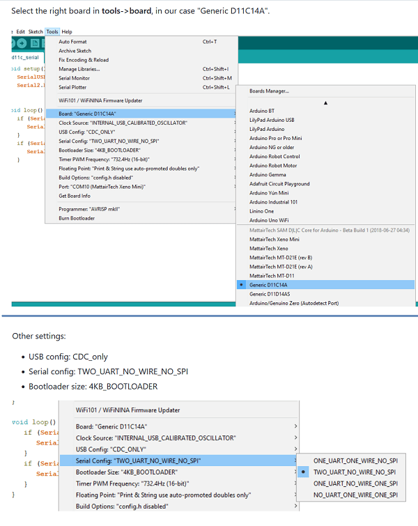 Be careful to have the right settings in the Arduino IDE before trying uploading code
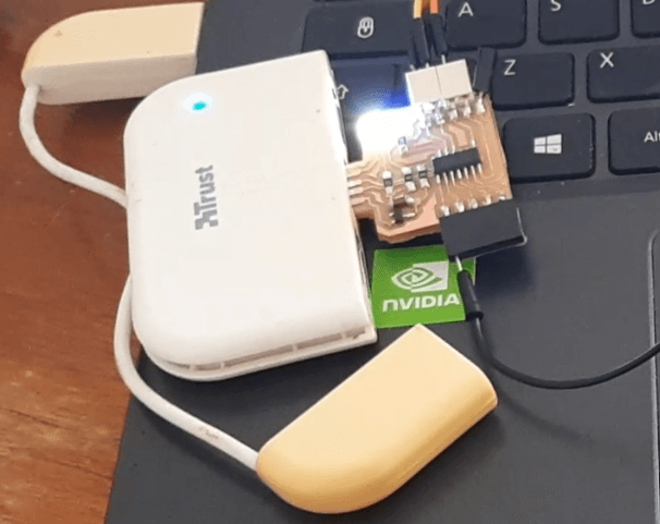 image of my programmed Board blinking
Input sensor module
I then repeated the same process, creating another PCB board and stuffing just one button and one trimmer on it. My idea is to create modular boards,
and use them to test different functions of the main board (I ended up creating just one tho). For example, in this case I can test both digital input signals (Push-button), and analog signals (Trimmer).
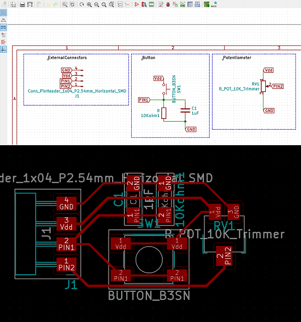 Kicad design image card
Debounce hardware
A particularity that I want to emphasize is the capacitor I added in parallel to the button pull-up resistor to create a button Debounce. Though for greater efficiency it would be better to use a shmitt trigger, I wanted however stay on a simple design.
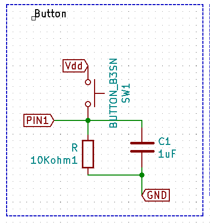 Debounce circuit on KiCad
I have reported below the simulation I made on Falstad website of the debounce circuit. What this circuit does?
When you release the button (and in this case ONLY when you release it), the output will not be instantaneously Zero, as it would be in a simple button circuit, but the capacitor prevents the undesirable impulses from the possible mechanical oscillation of the button.
In short the output signal tends to Zero not instantaneously but gradually with some delay.
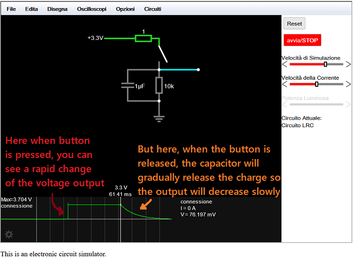 Debounce Simulation
I therefore set this signal output delay to a typical value of 50ms, which is an average time to dissipate all the mechanical oscillations of the button.
For the calculations I used the equation of a discharging capacitor:
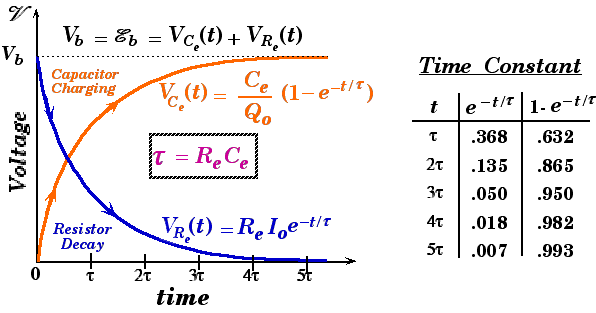 Charging and Discharging Capacitor Formulas
Basically, a Capasitor dicharging (or Charging) time, depends on the Resistence of the circuit and the Capacity itself, to complitely discharge the Capacitor in the above circuit you need to wait 5 times the value of RC, so to have a debouncing time of 50ms I just choose a Capacitor of 10uF and then calculated with a reverse formula that I would need a Resistor of 5kOhm.
I then want to show how I enjoyed putting a logo on the board on Inkscape ed to create a particular outline.
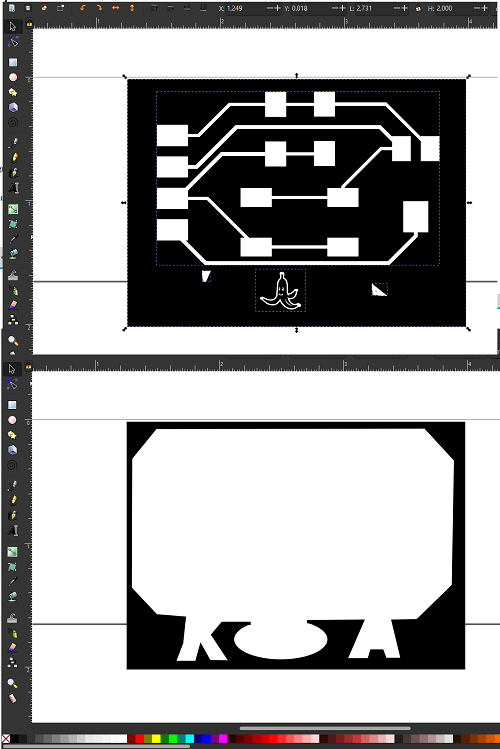 Trace and outline of the module, inkscape
Koa would be my nickname that my old roommates gave me when I lived there in Rome, it would be the central part of my name: MarKOAntonio.
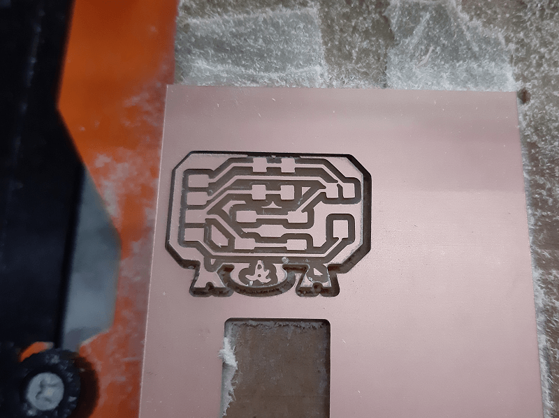 The fresh milled module
Finally, here is the module connected and the main board:
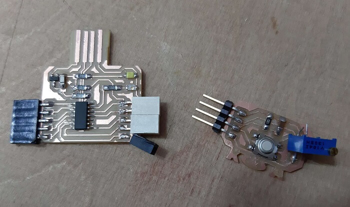 PCB SAMDUINO and the input module
Making my own Arduino Uno
This is an experience I did during the Input Device week, but I want to put it here because it suites the topic more.
I've always wanted to make my own Arduino ever since I burned the first Arduino Uno (the first of a long series) and I was wondering if it was possible to at least reuse the AtMega chip.
 some of my burned Arduino Uno boards/ AtMega318 chips
In my case some of the AtMega318 taken from burnt out Arduino Uno boards were still working.
To carry out this project I referred to the official guide (link page) of how to make an Arduino on Breadboard.
 Arduino on breadboard web page
Luckly very few components are required for a minimal board design
Components list
I also made other researches, for example about the AVcc and how to power the Analog Circuitry at best, like is shown in the following topic reply.
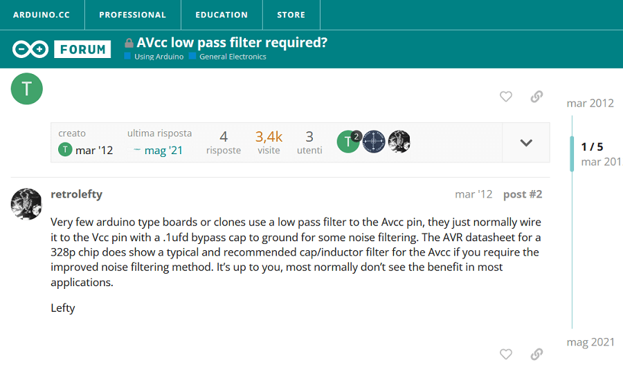 The need of another Capacitor for the AVcc
Even so few components, I managed to end up with a lot of failings with this project, I'm not gonna describe all of them in details ('cause this page is already very long) but just put some pictures with minimal descriptions.
Anyway this is the story of my own Arduino's that I called: Marcuino
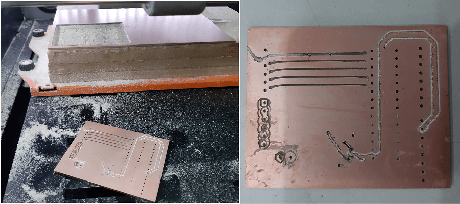 I attempt, after flip the board to mill the other face, the tape couldn't hold the board correctly
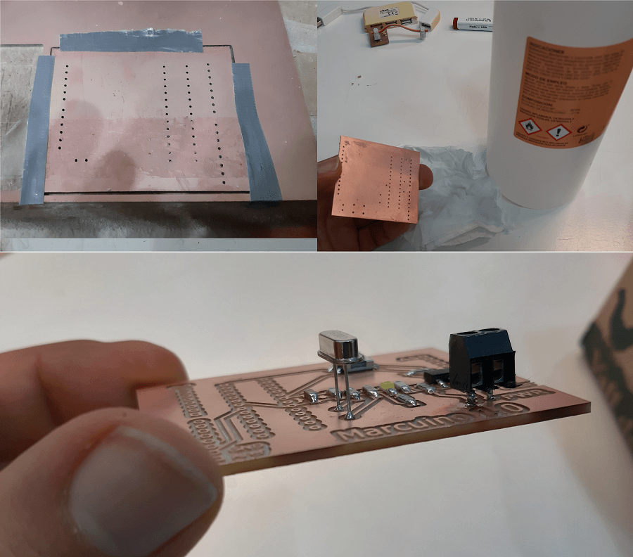 II Attempt, managed to mill it correctly but then realized that some components were badly located for soldering
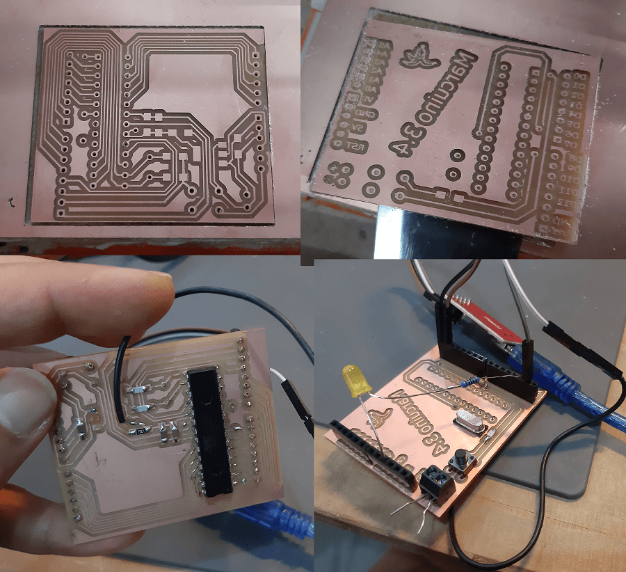 III Attempt, managed to easily solder all the components, still some component placing mistakes, but the voltage regulator circuit failed the smoke test
3.4 was not the version number, but the number of ages this project took until then to be done :(
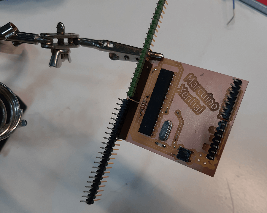 IV Attempt, get rid of not essential components (that's why Marcuino Xential), BUT I then realized I was following a wrong guide and the Oscillator was not connected correctly
A classmate of mine, instead of Marcuino Xential, used to call it Marcuino Henital, so funny.
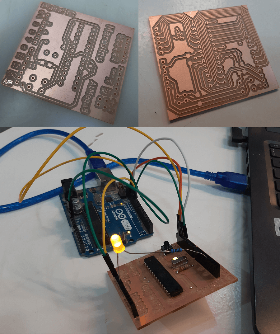 V attempt, the final one
Below you can see the final schematic and PCB traces
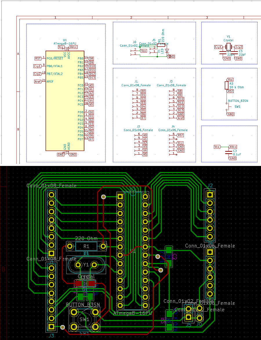 Schematic and Traces
In order to put the female sockets at the exact same place of a standard Arduino UNO is very useful use the Rule. You can find it under the Inspection Menu.
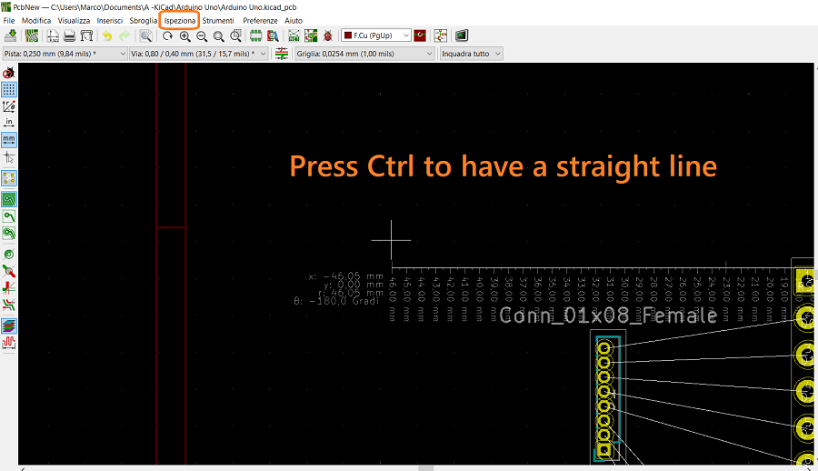 KiCad Trick
Here the Inkscape customization:
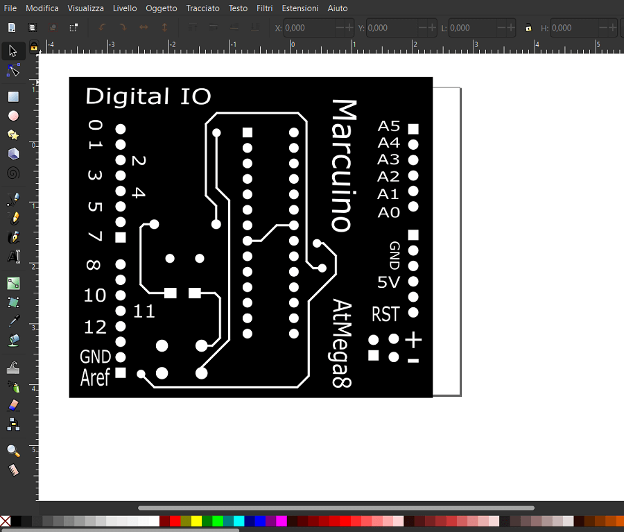 Customizing my Marcuino board
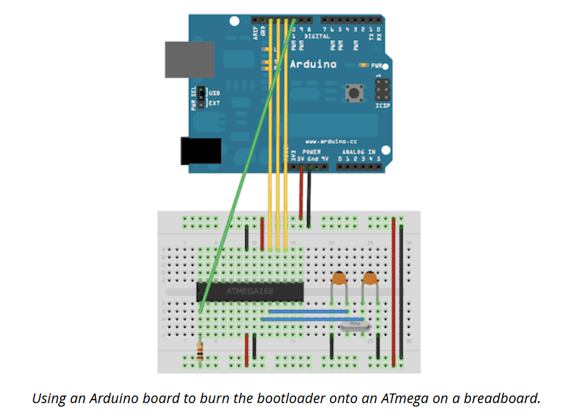
Burn the bootloader with an Arduino Uno
once you have your physical PCB board with an AtMega chip, you could program it with the aid of an Arduino Uno used as a Programmer or, if the chip is brand new, you need to first burn a bootloader.
I will explain how I proceeded to burn a bootloader and upload my first Blink sketch on the Marcuino with the AtMega8 using an Arduino Uno as a programmer.
First, I uploaded the ArduinoISP sketch you find in the examples folder of the Arduino IDE into the Arduino UNO.
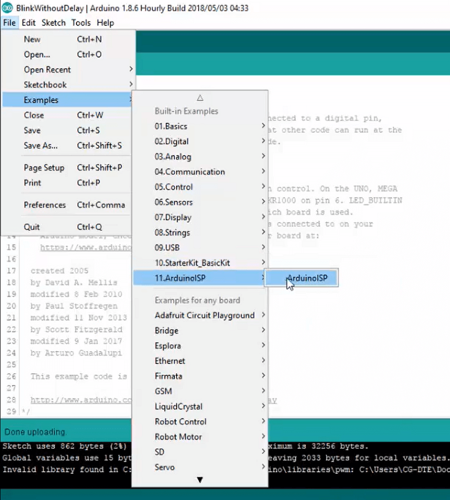 Compiling ArduinoISP sketch
This way you are starting setting the Arduino UNO as a Programmer, so you can connect to the target board (in my case the Marcuino) as indicated in the picture below:
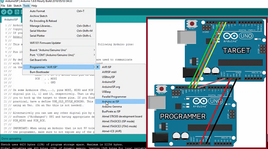 Programmer and Terget Board electrical connections
Finally, you select the lest setting for the Target board, in this case the chip to program is an AtMega8, and then click on Burning Bootloader, wait until the IDE indicates the process is complited.
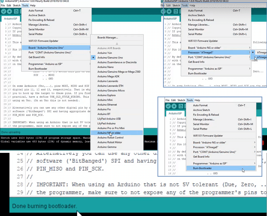 Burning the Bootloader
To upload a generic code, keep the same electrical connections between Programmer and Target Board and the same board settings. Just choose the program you want to upload and then go to Sketch -> Upload using a Programmer.
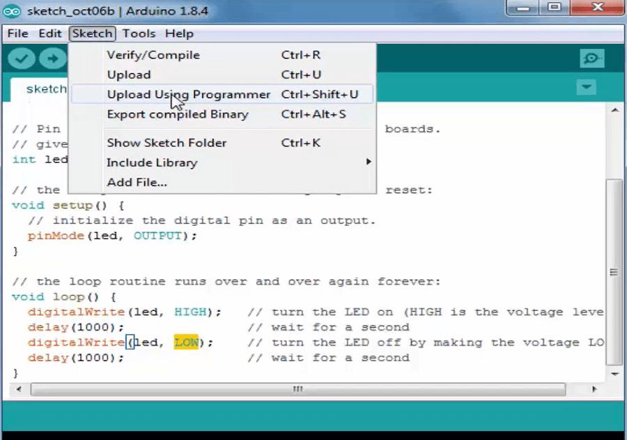 Uploading using a Programmer
How Create a doble side PCB and putting Via Connections
WIth a doble side PCB as It's the Marcuino I happly improved my knowledge in manufacturing Electronics boards.
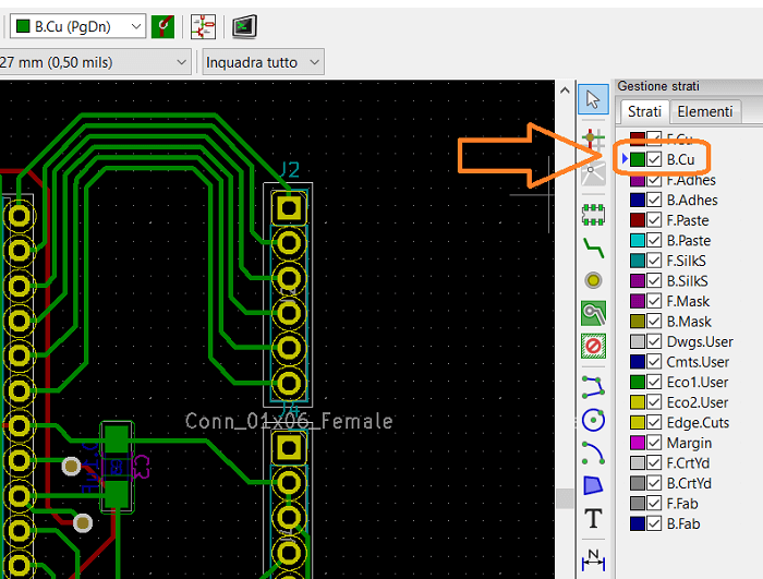
To do that, first you need to design your PCB accordingly, on KiCad you can flip the components on the other side (pressing F) and consequently set the bakward traces on the side menu, those will be green to differentiate from the red front traces.
 Backward Traces on KiCad
Once you are satisfied with the result, export the whole file as usual, with an .SVG extension, selecting both the front and backward faces. On the InkScape side you are gonna add at least 2 more layers: BackwardTraces and Holes to the 3 standard layers we generally use Backgroud, Outline and FrontTraces
Now that you have your dobleside PCB, let's put some Via in it.
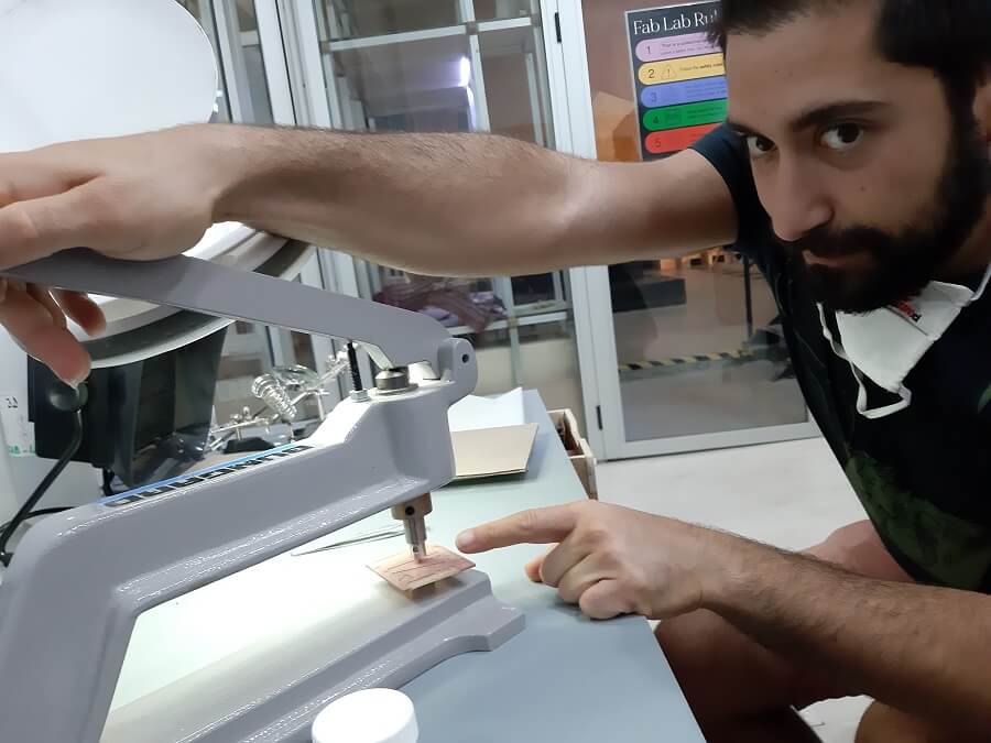 Me putting a Via with the proper tool
In order to do that, you need a special tool, like the one in the picture above.
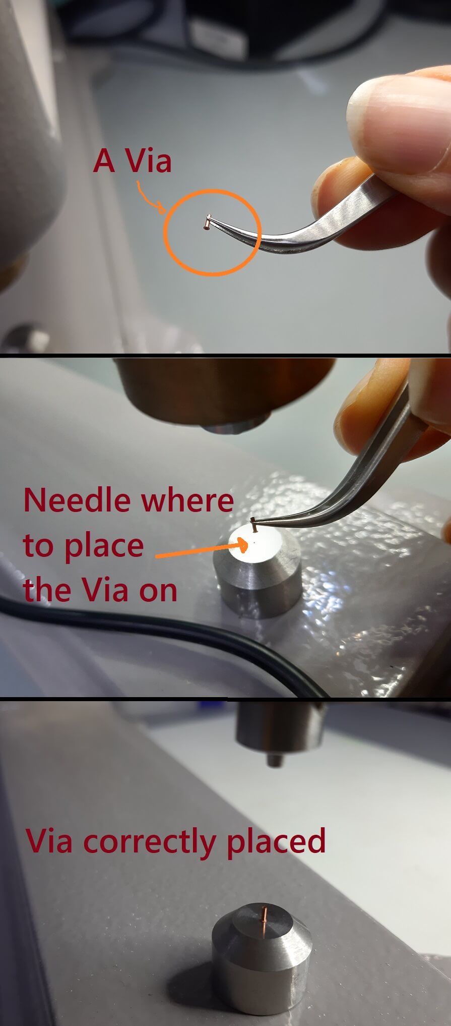 A via and where to place it
Basically, a Via is just a very tiny tube of copper, that you carefully place on the needle that keep it fix in place.
Then, as showed below, you put the PCB on, align its hole on the Via. Once the Via is inserted, you can press it.
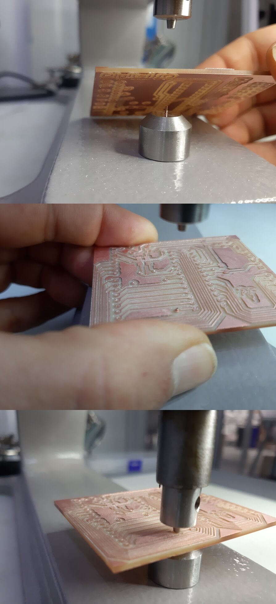 Inserting the Via in the PCB board
You finish putting some solder on them to keep them in place.
The whole thing can be very frustrating and very time consuming at the beginning because it is about maneging very small things, but after a while I became a pro and could place Vias in a matter of seconds.
APPENDIX
How Create a new Customized Component in KiCad
In order to create a new component in KiCad, there are basically 2 steps to follow:
First, create a New Symbol, you can do it in the main view of the software by clicking on the specific button. The Symbol Editor Page will appear and there you can create a new Symbol in a specific library (fab in my case) using the side menu bar where you can place input/output pins, geometrical drawing and Text.
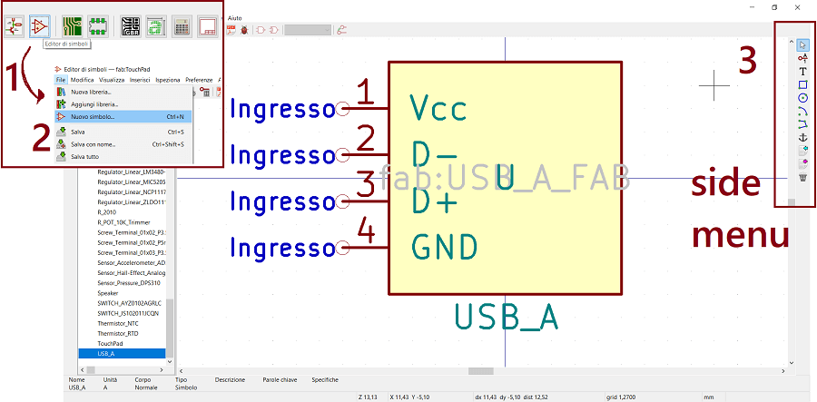 Symbol Editor steps
Once that, the second step is about creating and associating the Footprint.
Back on the main view of the sw and by clicking on the Footprint Editor button, the editor page will appear as well. You then create a new footprint (if you need it, otherwise you can associate it with some already done footprint) and you name it (with the same name you gave to the Symbol you created before).
After that, the side bar menu would active and you can place the first Pad, the default is a through Hole Type (THT), but you can modify the property, the shape and the distances between them.
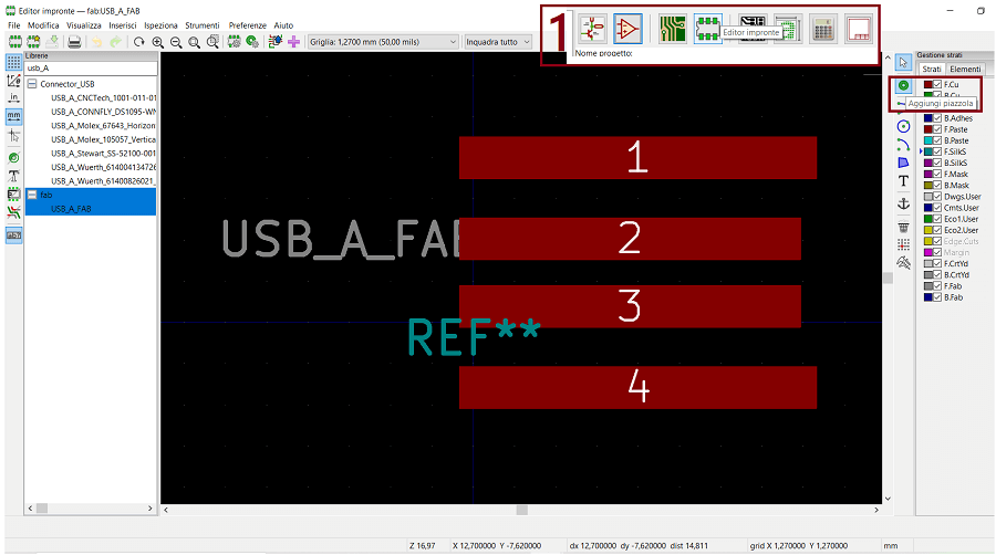 Footprint Editor steps
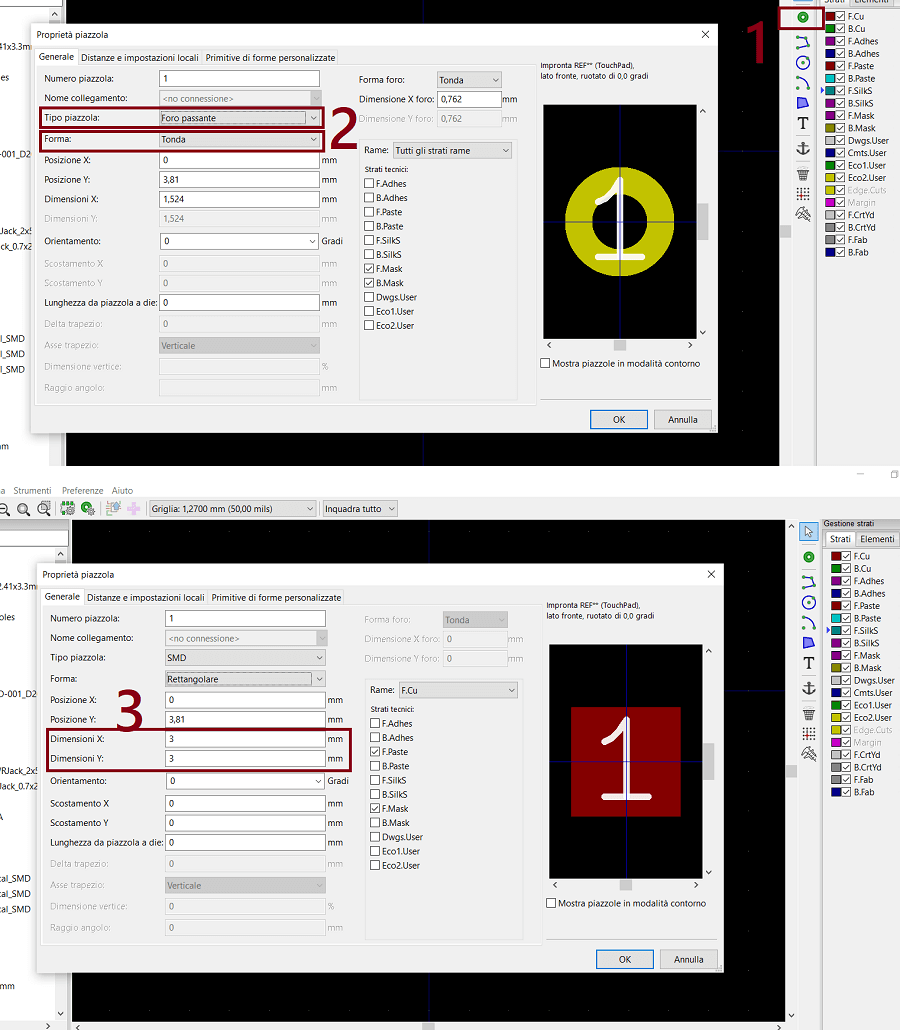 Pad editing menu
In my case, I had to carefully measure with a caliber the dimentions and distances of the Pads in a real USB type A connector and apply them in the Editor.
In the end you save the new footprint in a specific library (still fab in my case) and finally you go back to the Symbol in the Symbol Editor, go to Edit -> Properties and associate the footprint.
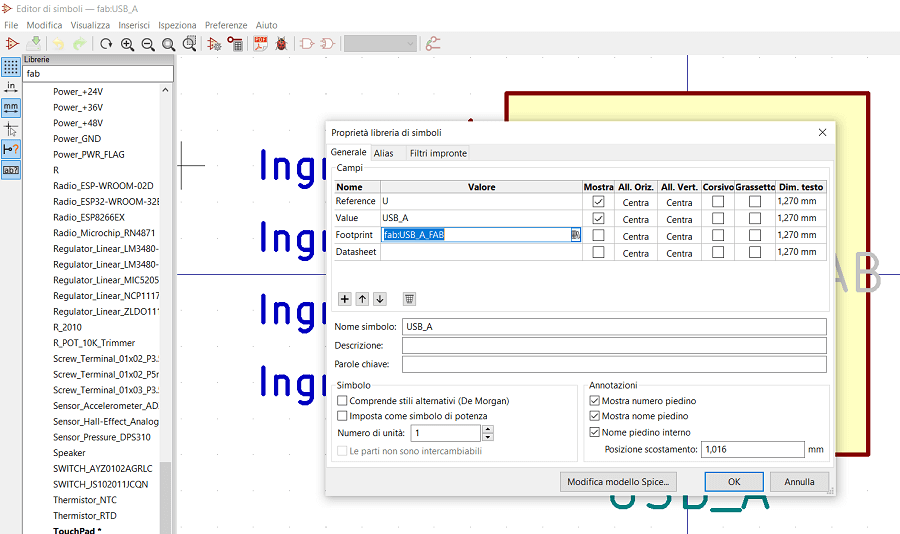 Editor Symbol's Properties menu and Footprint association
Now, you have your new component ready to use for future projects.