7. Electronics design
This week I learned electronics design in KiCAD, and double sided PCB manufacturing
Group assignment
You can find the group assignment page here. I am applying KiCAD and MCB milling below.
KiCAD
KiCAD is an open source Circuit and PCB design software. For an open source software, KiCAD seems to be very popular even in professional settings. Indeed, the electronics department at my company uses KiCAD, so learning it will be quite useful for me as well.
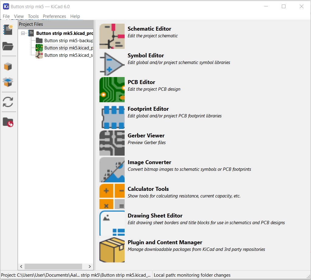
After loading and installing KiCAD. one is met by the main screen:
The first step was installing the custom libraries provided by fab academy. These are a convenient way of accessing all the components available at fablab, all in ope place. In addition, the fablab components have pre-assigned footprints and even 3d models!
The actual design work starts with the schematic editor. Here, components in schematic form are placed out, and electrical connections are routed between them, either as actual conduits or as flags. The schematic editor assigns numbers to the components, and performs an electrical rules check.
After the schematic is done and cleared by the rules check, the next step is the PCB editor. Here the components are actually represented as their footprints, placed on a PCB and routed with actual traces.
The components are at first dropped in as a “ratsnest”, essentially a big pile with lines representing the connections from the schematic.
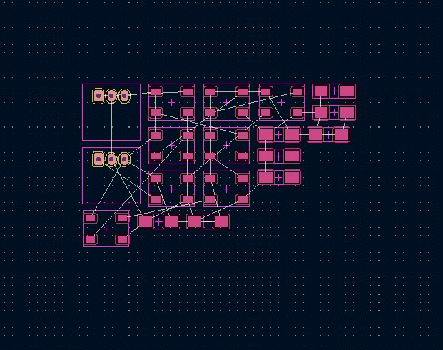
The components can then be moved around to their final spots, and connected with traces on the PCB.
The PCB outline can either be drawn in KiCAD itself or imported as a DXF file. The import function makes it quite easy to integrate with 3D CAD workflow.
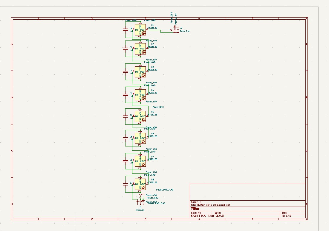
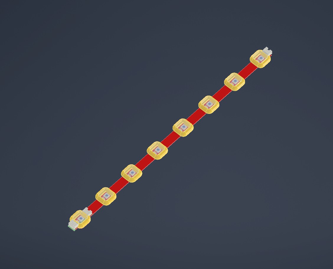
For example, I’ve been working on my LED button project in KiCAD
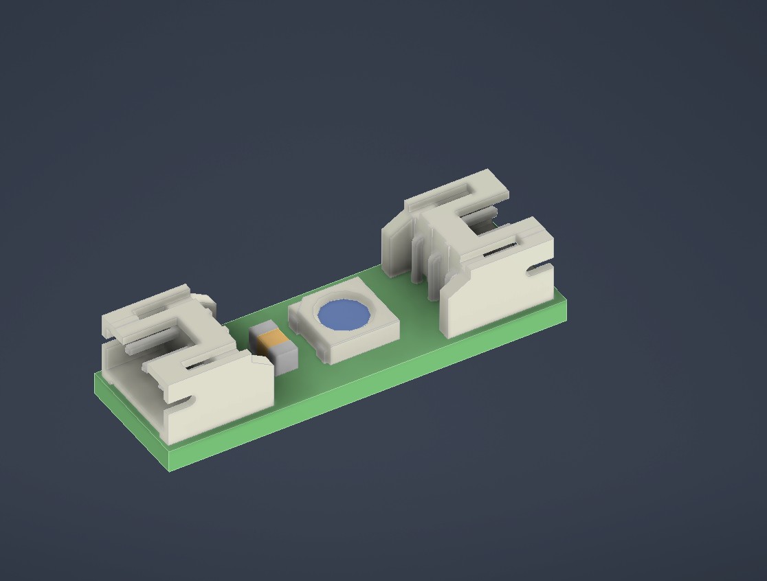
I modelled a 3D printed and laser cut model for the button, around a simple board exported from KiCAD. I will need both two single buttons, and one strip of 8. The strip of 8 was developed from the single button.
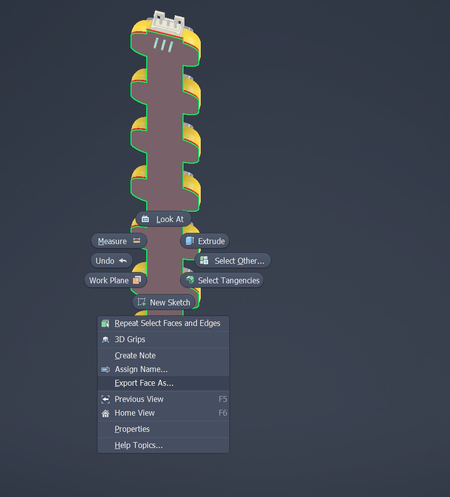
From here, I can export the full board as a DXF from inventor back to KiCAD
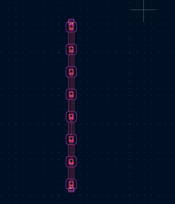
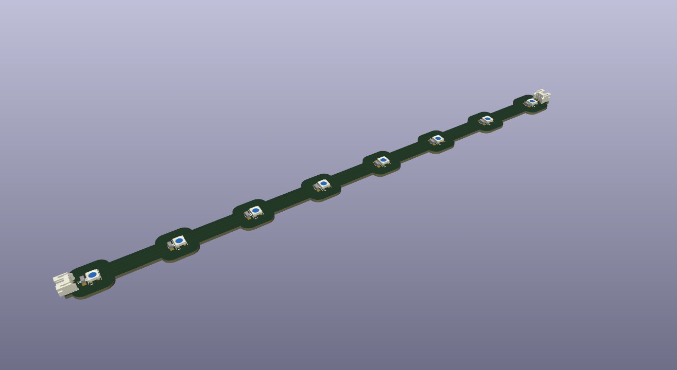
Back in KiCAD, here is the complete board.
This board will be made with the vinyl cutter flexible board method, so trace density is intentionally quite low.
Double layer PCBs
When designing PCBs in KiCAD, it quickly becomes apparent, that single layer boards have significant limitations. There is fortunately a solution: double layer boards!
Double layer boards look exactly like single layer ones, except that they have copper on both sides of the substrate. The board can then be milled from both sides, essentially doubling the board space.
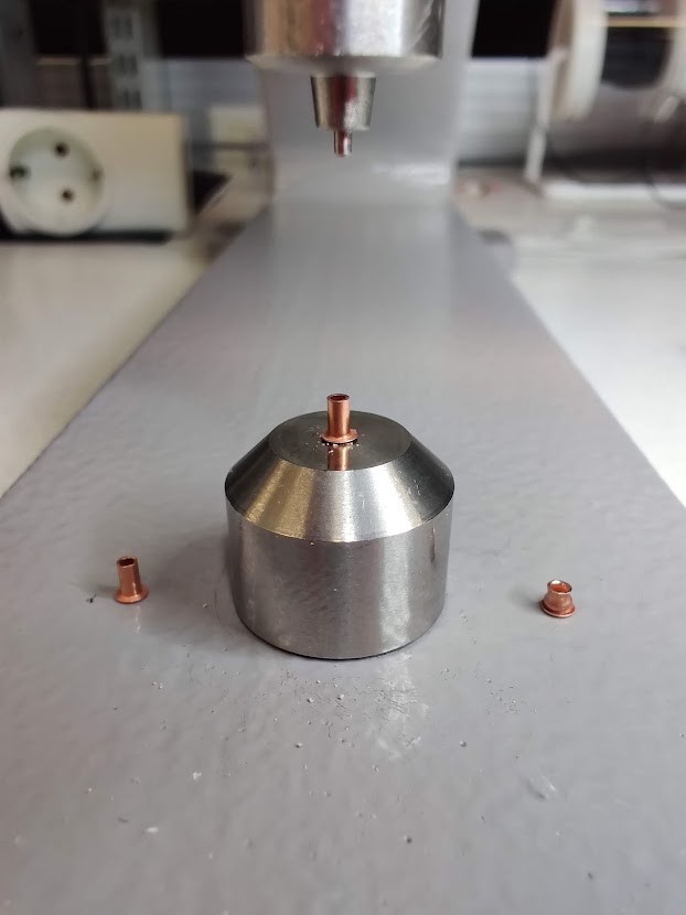
This of course wouldn’t make much difference if the board sides couldn’t be interconnected. Fortunately, they can. This is done using vias, tiny copper rivets that are pressed in little drilled holes in the PCB.
Attiny 412 board
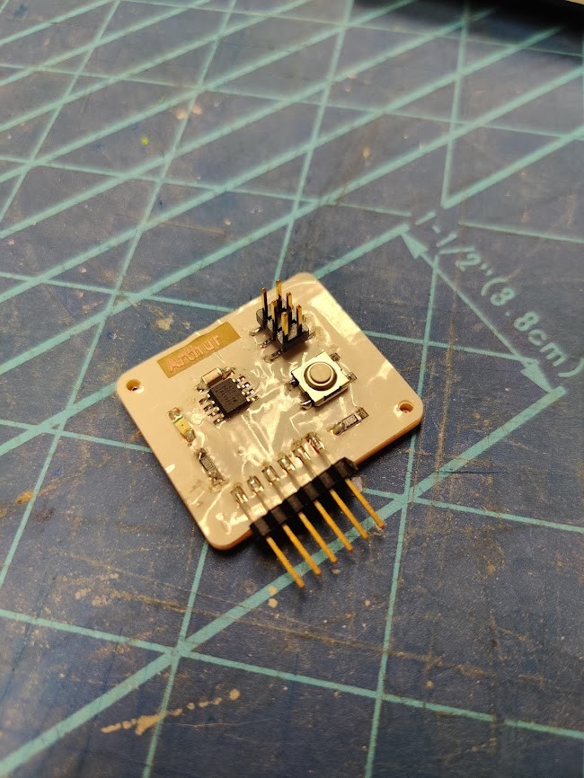
For the weekly assignment, I set out to design a simple microcontroller board, with a led and a push button. The microcontroller used is the attiny 412, a mere 8-pin IC with a full on programmable microcontroller!
I think it might have been theoretically possible to make the circuit with a single sided board. However, going double sided really made the process a lot simpler.
In a simple case like this, I could next time use the bottom layer entirely for ground. In that case, the bottom could be left unmachined, with vias connecting ground traces between the bottom plane and components. In essence, we would have a double sided board, but only need to machine one side!
PCB milling
The board machining process went as follows:
- Engrave upper side with 0.2mm V-mill
- Drill via holes w 0.8mm drill
- Drill mounting holes w. 2mm drill
- Upper side hatching with 1mm flat mill
- Outline cut w 1mm flat mill
- Flip and align board.
- Lower side hatching, 1mm flat mill
- Lower side engrave, 0.2mm V-mill
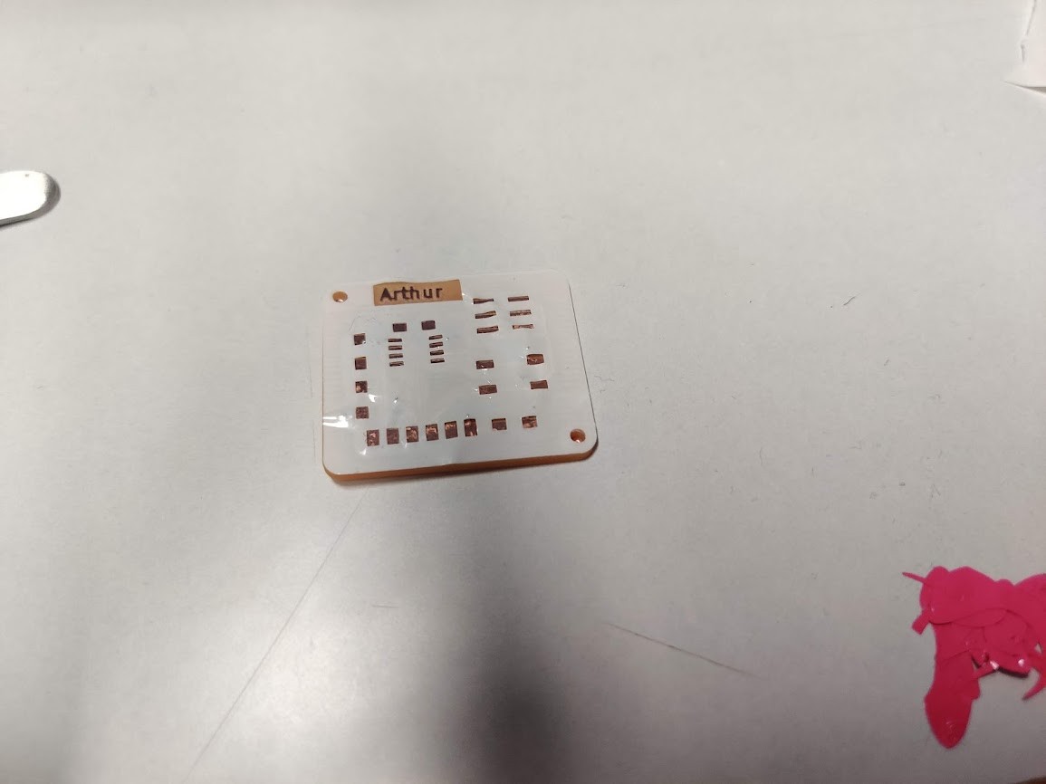
Here’s the board after milling.
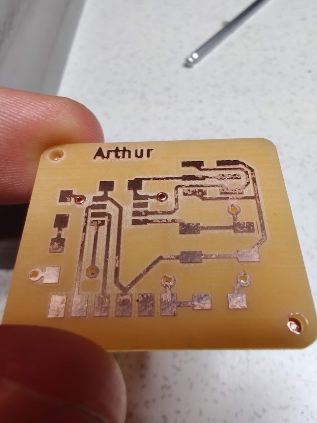
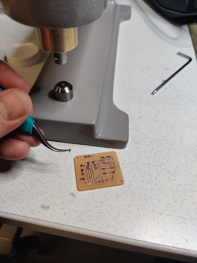
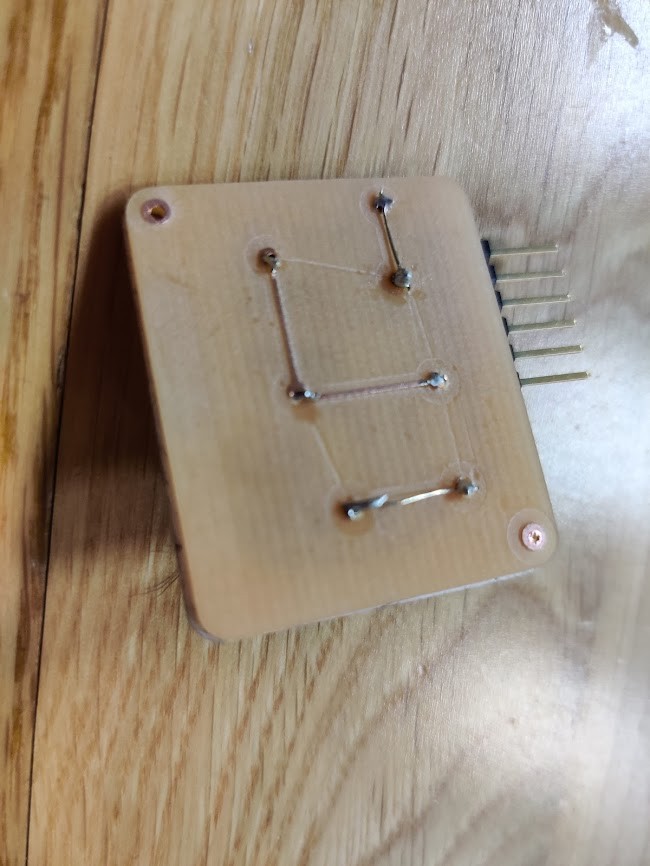
The miling process generally went okay. The drill holes ended up a bit too shallow, so i decided to redrill them from the opposite side. This time however, my z-position seems to have been messed up, so the travels ripped out the traces! Ive gone too far to redo the board, but i have an alternative solution. Que meme.

I’ll just manually solder the vias together. No biggie.
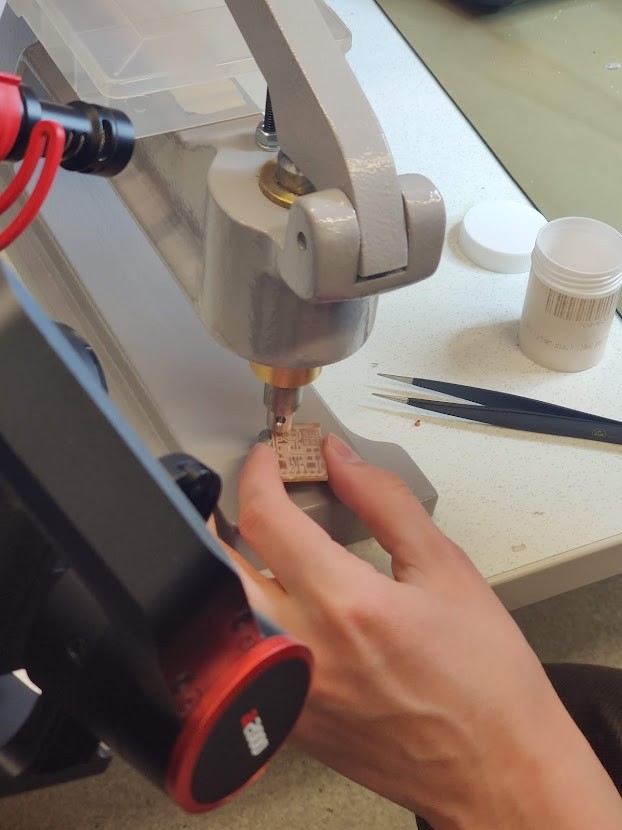
Speaking of vias, those need to be installed. The vias use tiny 0.8mm rivets, that are attached to the board using a punch press.
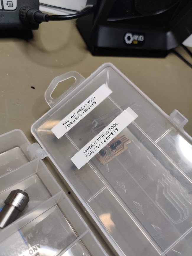
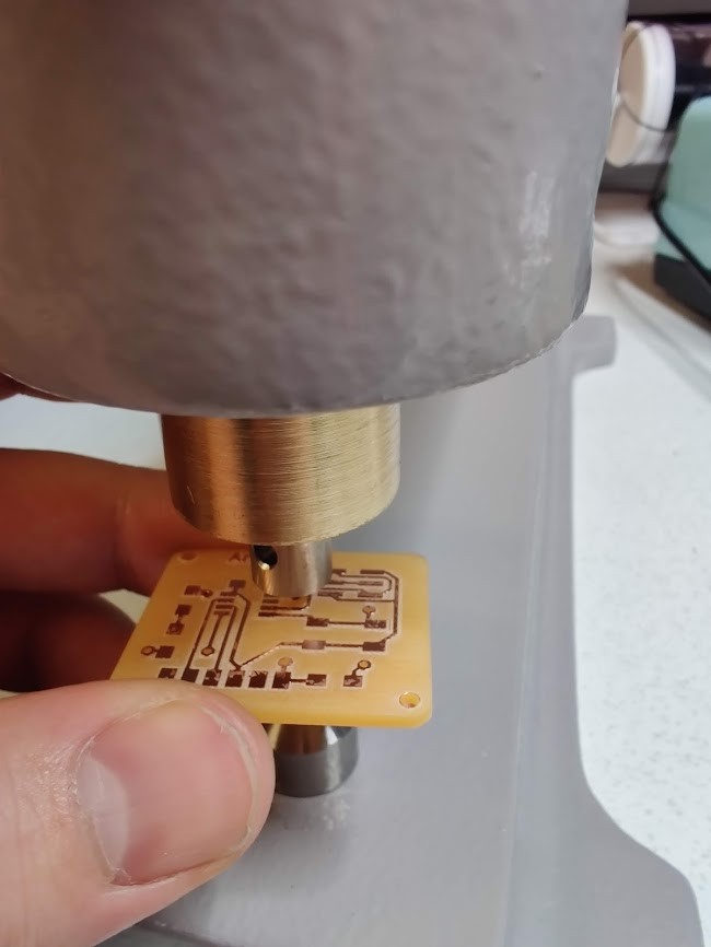
This step was easy, except that I kept loosing the tiny rivets!
Solder mask
I noticed during week 5 that most of my issues when producing boards were caused by solder unintentionally shorting random traces, especially a problem with traces under components. To prevent this from happening this time, I decided to create a solder mask
A solder mask is simply a layer, that masks everything except the pads for the component sbeing soldered to the board, hence the name. Creating a solder mask is easy, KiCAD can readily export them in various formats from the “plot” menu.
There are multiple ways to actually manufacture a solder mask. Seeing that I have access to the vinyl cutter and heat resistant material, I decided to try that route, using 3M-1.
The vinyl cutter ran with 100g force and 4cm/s. This gave quite good results.
After weeding, the 3M-1 was glued to the board using its inherent sticking action.
The vias were left under the solder mask, but protrude slightly, thus making the mask a bit uneven. KiCAD has an option to leave the vias uncovered. This could alleviate the problem. The mask remains equally functional though.
Soldering
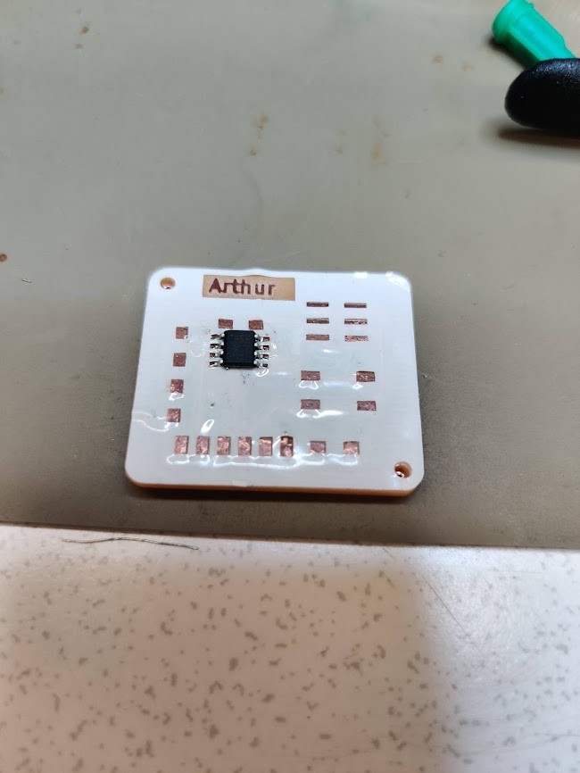
Learning from last time’s experience, I mostly used solder wire and the iron this time, except for the 412 itself, which was soldered using paste and hot air.
The electrical wire available was quite big for the vias, I instead used the individual strands from that.
Incredibly, the components were correctly soldered after the first time! Go solder mask! My only problem was that one of the soldered vias had proken loose, resulting in a bad connection. This was easy to fix.
Programming
See week 9 for my programming shenanigans.
You can find this week’s design files here