WEEK 16 - System Integration
Final Project Case for PCB Integration
Direct Link to Final Project
This System Integration assignment is directly connected to my final project, OrquiWall Smart System. This page documents one of the required integration stages of the final project, where the electronics, PCB, A4988 driver, wiring, packaging, sensors, actuator and final assembly are organized as part of the complete working system.
Please review the complete final project documentation here:
Assignment Checklist Evidence
- Made a plan for system integration for my final project.
- Documented the plan with CAD and sketches.
- Implemented methods of packaging.
- Designed the final project to look like a finished product.
- Documented system integration of the final project.
- Linked this documentation with my Final Project page: this Week 16 System Integration documentation includes a direct link to my Final Project page so the integration work can be reviewed in context.
- Tracked the progress of my project.
- Specified the country of origin of materials and components.
- Tested the integrated system by checking fit, wiring, packaging, sensor connection and motion logic.
- Documented the final project as a complete working system.
- Documented final assembly design adjustments.
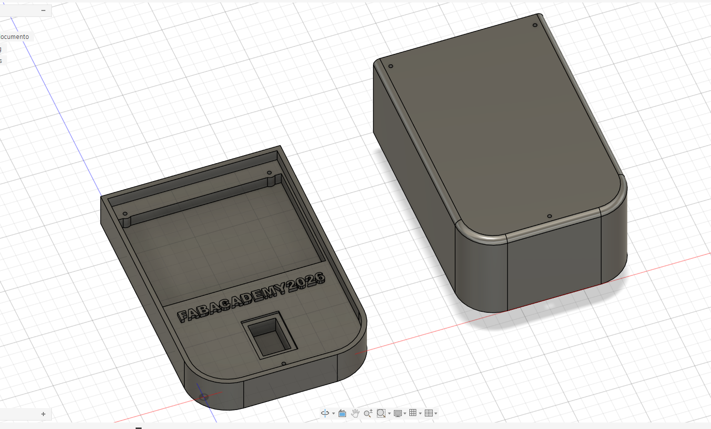
The goal of this week was to integrate the electronic system of the final project into a physical enclosure. For this stage I designed a custom case for the PCB developed for the final project. The case was modeled in Fusion 360 and fabricated in PLA using a Bambu Lab X1 Carbon 3D printer.
The enclosure was designed to hold the main PCB and also leave internal space for an A4988 driver and its wiring. The case includes cable exits so that the electronic system can connect to external devices without forcing or bending the cables inside the box.
Connection with Final Project
This System Integration assignment is directly connected to my Final Project because it documents how the electronics were packaged, organized and prepared to become part of the complete OrquiWall Smart System. The work shown on this page explains how the final project PCB, A4988 driver, wiring, cable exits and PLA enclosure were integrated as one physical electronic module.
This connection is important because the final project is not only an electronic circuit or a mechanical structure; it is a complete system where the PCB, sensors, motor driver, actuator, wiring, enclosure and irrigation mechanism must work together. For this reason, this documentation should be reviewed together with the Final Project page.
1. Assignment Requirements and Questions Answered
This section explains how my Week 16 documentation answers the System Integration assignment requirements. The objective of this assignment was to design and document how the different parts of my final project come together as one complete system.
| Assignment Question | How I Answered It in My Final Project | Where It Is Documented |
|---|---|---|
| Made a plan for system integration for your final project? | Yes. I divided the OrquiWall Smart System into subsystems: mechanical system, motion system, electronic control system, sensors, user interface, power and wiring, packaging and final system integration. This helped me define how each part connects with the others. | Section 3: System Integration Plan |
| Documented your plan with CAD and/or sketches for system integration? | Yes. I documented the Fusion 360 CAD process used to design the PLA enclosure for the PCB, A4988 driver and cable routing. The page includes the final CAD model, dimensions and printed case evidence. | Sections 7, 8, 9 and 10 |
| Implemented methods of packaging? | Yes. I implemented a two-part PLA enclosure with a base, removable cover, internal PCB area, space for the A4988 driver and side cable exits. The electronics are placed in a dedicated area instead of being exposed on the workbench. | Section 11: Packaging Method Implemented |
| Designed your final project to look like a finished product? | Yes. The enclosure gives the electronics a cleaner and more protected appearance. The rounded corners, removable cover, defined cable exits and organized internal layout make the electronic module look closer to a finished product. | Sections 11, 12 and 13 |
| Documented system integration of your final project? | Yes. I documented how the mechanical structure, PCB, A4988 driver, wiring, sensors, motor system, display and PLA enclosure are integrated into the OrquiWall Smart System. The system is already working as a complete prototype for automated orchid immersion irrigation. I also included system integration testing, complete system integration and final assembly design adjustments to show how the final project works as one unified prototype. | Full Week 16 documentation, especially Sections 3, 4, 6, 11, 13, 15 and 16 |
| Linked to your system integration documentation from your final project page? | Yes. This page includes a direct link to the Final Project page. The Final Project page should also include a return link to this Week 16 System Integration page so the evaluator can review both documents together. | Direct Link to Final Project, Connection with Final Project and Download Files sections |
Important note: System integration in this project is not only about putting the components together. It is about defining a dedicated place for each part, organizing the wiring, protecting the electronics, connecting the mechanical and electronic subsystems, and making the prototype look and work as a complete final project.
2. Integration Objective
The integration objective was to move from separate electronic tests to a more complete physical system. The PCB, driver and wiring need protection, organization and a defined position inside the final project. The enclosure helps make the electronics easier to transport, safer to handle and cleaner to connect.
| Requirement | Design Response |
|---|---|
| Hold the final project PCB | The base includes a rectangular internal area sized for the PCB. |
| Include A4988 driver and wiring | The case leaves free internal volume for the driver module and cable routing. |
| Allow cable exits | Openings were added to route external cables without compressing them. |
| Protect electronics | The enclosure walls separate the PCB from external handling and accidental contact. |
| Be printable in the Fab Lab | The design was prepared for PLA printing on a Bambu Lab printer. |
| Look like a finished product | The rounded case, removable cover and organized wiring make the electronic module cleaner and more finished. |
3. System Integration Plan
Before integrating the final project, I divided the OrquiWall Smart System into smaller subsystems. This helped me understand how each part should connect with the others and what needed to be tested before the final assembly. The integration plan was useful to organize the mechanical structure, electronics, sensor inputs, actuator movement, user interface and packaging as one complete system.
| Subsystem | Main Elements | Integration Objective |
|---|---|---|
| Mechanical system | MDF wall frame, 3D printed supports, reservoir, orchid pot, guide system, lead screw and bearing holders. | Support the orchid and allow the reservoir to move vertically for the immersion irrigation process. |
| Motion system | Stepper motor, A4988 driver, lead screw, guide rods and upper/lower limit switches. | Move the water reservoir up and down safely, stopping at the correct positions using the limit switches. |
| Electronic control system | Custom PCB, XIAO ESP32C3, resistors, capacitor, screw terminals, headers and power connections. | Organize the electronic connections and control the sensors, motor driver and display from one main board. |
| Sensor system | Capacitive humidity sensor and water level/contact sensor. | Read the substrate moisture condition and verify the water/reservoir state before activating the irrigation sequence. |
| User interface | OLED/LCD display and system status messages. | Show the user the current state of the system, such as dry substrate, wet substrate, moving up, irrigating and moving down. |
| Power and wiring | 12 V power supply, motor wiring, sensor cables, display cables and PCB connections. | Provide energy to the system and organize the cable paths to avoid loose or exposed connections. |
| Packaging | 3D printed PLA enclosure, removable cover, PCB tray and side cable exits. | Protect the PCB and A4988 driver, organize the wiring and separate the electronics from the water and plant area. |
| Final system integration | Mechanical structure, electronics, sensors, actuator, display, wiring and enclosure. | Combine all fabricated and electronic parts into one functional prototype for automated orchid immersion irrigation. |
Integration strategy: I first tested the electronic components separately, then placed the PCB and A4988 driver inside the printed enclosure. After that, I routed the cables through the side exits and connected the module to the mechanical structure, sensors, motor and display. This process helped me verify the system step by step before the final assembly.
4. Track the Progress of My Project
To track the progress of my final project, I used the same subsystem division from the integration plan. This allowed me to identify which parts were already completed, which ones were still in progress and what actions were needed before the final system test.
| Subsystem | Progress Status | Evidence / Result | Next Action |
|---|---|---|---|
| Mechanical system | Completed and integrated | MDF wall frame and 3D printed supports were designed, fabricated and assembled with the movement system. | Continue observing alignment during repeated irrigation cycles. |
| Motion system | Working | The stepper motor, A4988 driver, lead screw and limit switches move the reservoir up and down during operation. | Improve smoothness and reliability for long-term use. |
| Electronic control system | Working | The custom PCB was designed, fabricated, soldered and integrated with the PLA enclosure. | Improve connector labels and cable organization in the next version. |
| Sensor system | Working | The humidity sensor reads the substrate condition and supports the irrigation decision. | Continue refining threshold values according to orchid substrate behavior. |
| User interface | Working | The display shows the main system states during the irrigation sequence. | Improve final messages and visual feedback if needed. |
| Packaging | Implemented | A two-part PLA enclosure was designed in Fusion 360 and printed for the PCB and driver. | Improve the next version with connector labels, mounting holes or ventilation if needed. |
| Final integration | Working as complete prototype | The system reads humidity, activates the motor, moves the reservoir, stops with limit switches and shows status on the display. | Continue testing repeated cycles for robustness and final presentation. |
Progress tracking conclusion: The project advanced from isolated tests to a complete working integrated prototype. The main subsystems are connected and functioning together, while the next improvements are focused on reliability, cable labeling and repeated cycle validation.
5. Materials and Components Origin
As part of the sourcing and planning process, I identified the origin of the main materials and components used in the system integration stage. Some components were locally available in Ecuador through the Fab Lab or local suppliers, while other electronic modules are internationally manufactured and commonly distributed through electronics suppliers.
This information helps evaluate availability, replacement options, fabrication constraints and the possibility of making more parts locally instead of buying them.
| Material / Component | Function in the System | Country of Origin / Source | Planning Notes |
|---|---|---|---|
| PLA filament | Used to 3D print the electronics enclosure, base and cover. | Available locally in Ecuador / commercial filament supply. | Selected because it is easy to print, rigid and available in the Fab Lab. |
| PCB material | Base material for fabricating the custom electronic control board. | Commercial PCB stock available in Ecuador / Fab Lab inventory. | Used to fabricate the board locally instead of buying a complete commercial control board. |
| Seeed Studio XIAO ESP32C3 | Main microcontroller for reading sensors and controlling the system. | China. | Compact size, Wi-Fi capability and compatibility with Arduino IDE. |
| A4988 stepper motor driver | Controls the stepper motor used for the vertical movement system. | China / international electronics supplier. | Common and accessible driver for small stepper motor control. |
| Stepper motor | Actuator used to move the reservoir through the lead screw mechanism. | China / international electronics supplier. | Selected because it allows controlled movement and positioning. |
| Lead screw | Mechanical transmission element for vertical movement. | China / international mechanical component supplier. | Used to transform rotational movement into linear movement. |
| Capacitive humidity sensor | Reads the moisture condition of the orchid substrate. | China / international electronics supplier. | Used as the main input for deciding when irrigation is needed. |
| Water level/contact sensor | Verifies the water or reservoir condition before irrigation. | China / international electronics supplier. | Used to support safer irrigation operation. |
| Limit switches | Detect upper and lower travel limits for safe movement. | China / international electronics supplier. | Important for preventing overtravel in the lifting mechanism. |
| OLED / LCD display | Shows the current state of the system to the user. | China / international electronics supplier. | Used as a simple interface for system feedback. |
| Resistors, capacitor, headers and screw terminals | Electronic assembly and connection elements for the PCB. | China / local electronics supplier in Ecuador. | Standard components used for soldering and wiring the final project PCB. |
| MDF board | Used in the final project structure and wall frame. | Ecuador / local material supplier. | Locally available material suitable for laser cutting and structural prototyping. |
| 3D printed supports | Mechanical support parts for the system structure. | Fabricated locally in Ecuador at Industrial FabLab UCuenca. | Designed and made locally using digital fabrication. |
Sourcing reflection: The project combines locally fabricated parts, such as the PLA enclosure, MDF structure and custom PCB, with imported electronic components such as the XIAO ESP32C3, A4988 driver, sensors and motor. This shows which parts can be made in the Fab Lab and which parts still depend on external suppliers.
6. System Integration Concept
The final project electronics are not only a PCB. They also include the driver stage, power and signal cables, and connections going to the external parts of the system. For this reason, the case was designed as an integration component rather than only a decorative cover.
The base of the case organizes the components, while the top cover closes the system. The design includes rounded corners to reduce sharp edges, screw holes for closing the case, and openings for cables. The internal layout separates the PCB area from the cable exit area so the wiring has a predictable path.
7. Measuring and Planning the Case
The first design step was to define the main dimensions of the enclosure. I used the PCB size, cable clearance and available space for the A4988 driver as references. The case footprint was planned around a rectangular electronic area with rounded corners and screw points.
The CAD model helped me define the relationship between the PCB, the cover, the walls and the cable exits before creating the printed enclosure.
8. Fusion 360 Modeling Process
After the 2D sketches were defined, I extruded the geometry to create the 3D enclosure. The design was divided into two parts: a base for holding the electronics and a top cover for closing the system. The base includes an internal recessed area for the PCB and space for the cable exit.
The corners were rounded to make the case easier to handle and to improve printability. Screw holes were placed so the cover can be aligned with the base. A rectangular opening was added as a cable outlet, allowing the wiring from the PCB and A4988 driver to exit the enclosure.
9. Cable Exit and Component Placement
One of the most important integration details was the cable exit. The PCB and A4988 driver require several wires, so the case needed openings large enough for cable bundles. The cable exit prevents the lid from pressing on the wires and gives the system a controlled connection point.
The base also includes internal space for the PCB and the driver. This is important because the A4988 needs room for its pin headers and wiring. The enclosure does not permanently hide the electronics; it organizes them so they can still be accessed during tests and debugging.
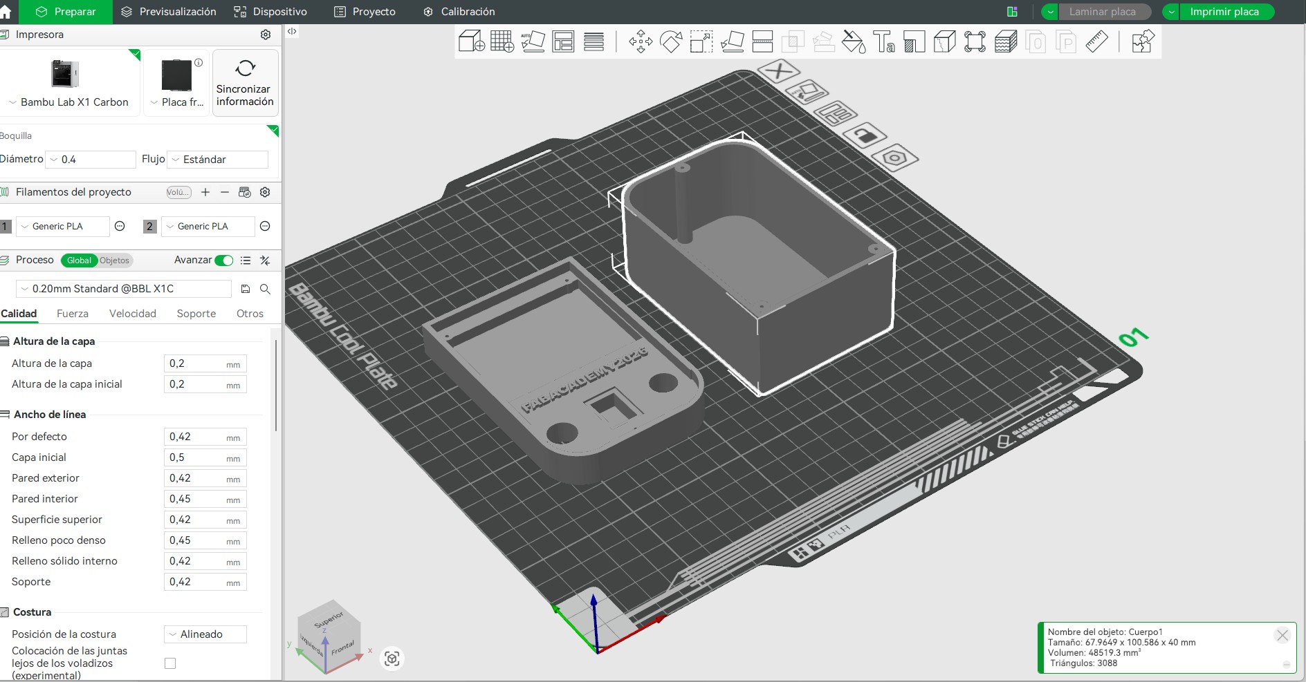
10. Preparing the Print in Bambu Studio
Once the model was ready, I exported the case for 3D printing and prepared it in Bambu Studio. The print was arranged on the build plate with the base and cover separated. The selected material was PLA because it is easy to print, dimensionally stable for this type of enclosure, and rigid enough to protect the electronics.
| Print Parameter | Value / Decision |
|---|---|
| Printer | Bambu Lab X1 Carbon |
| Material | PLA |
| Nozzle | 0.4 mm |
| Layer height | 0.20 mm standard profile |
| Parts printed | Case base and top cover |
11. Packaging Method Implemented
The packaging method implemented for this project was a two-part 3D printed PLA enclosure. The base works as the component tray for the PCB, A4988 driver and cable bundles, while the top cover protects the electronics from direct handling. This method was chosen because the case could be customized from the real dimensions of my board and quickly iterated in Fusion 360.
The enclosure is not only a box: it defines how the electronics are packaged inside the final product. The cable exits keep wires from being compressed by the lid, the internal space separates the PCB area from the driver and routing area, and the cover makes the module look more finished while still allowing inspection during tests.
| Packaging Decision | Reason |
|---|---|
| Two-part enclosure | Allows the PCB and wiring to be installed in the base and then protected with a removable cover. |
| PLA material | Fast to fabricate, rigid enough for a prototype case, and available in the Fab Lab. |
| Cable exits | Prevent wire compression and create a defined path toward the sensors, driver, motor and interface. |
| Rounded corners and screw points | Improve handling, make the case look like a finished product and help align the cover with the base. |
Packaging Methods Implemented
- Mechanical packaging: a custom PLA base and top cover package the PCB as a removable electronic module.
- Electrical packaging: the PCB, A4988 driver and cable bundles are grouped in one protected area instead of remaining exposed on the workbench.
- Cable packaging: side exits define where signal and power wires leave the case, avoiding pressure from the lid.
- Product packaging: the enclosure gives the electronics a cleaner final-product appearance and separates them from the water and plant area.
12. Finished Product Appearance
To make the project look more like a finished product, I focused on packaging the electronics instead of leaving the PCB, driver and wires exposed. The case has a defined shape, rounded corners, a removable cover and side cable exits. This gives the electronic module a cleaner appearance and makes it safer to handle during the final project tests.
The design is more than a simple box because it was created around the real integration needs of the final project. It includes a dedicated area for the PCB, space for the A4988 driver, a cable routing strategy and a cover that protects the electronics while keeping the wiring accessible.
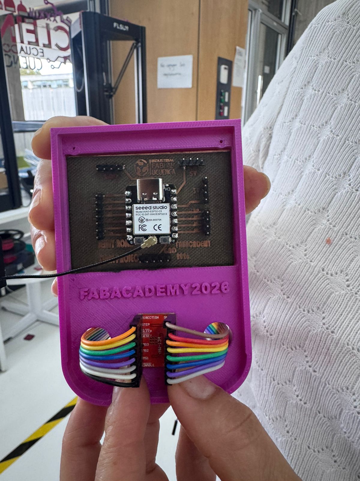
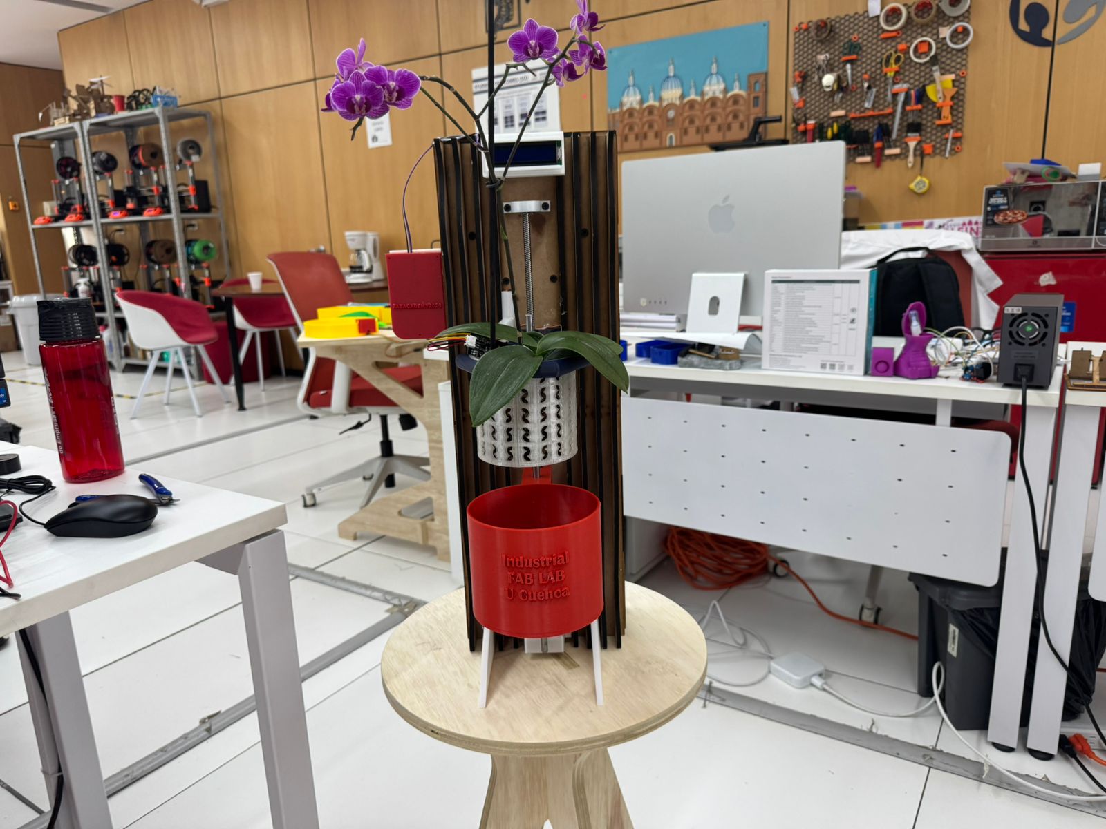
13. Hero Shot: Finished Product Integration
After printing the PLA case, I tested the real placement of the final project electronics inside the enclosure. The PCB sits in the internal area, the sensor connection remains connected to the XIAO ESP32C3, and the A4988 driver is positioned with the cables routed through the designed side exits.
These images document the system as an integrated product, not only as isolated parts. The goal was to confirm that the case could hold the PCB, allow the sensor and wiring to exit without pressure, keep the driver accessible and connect the electronic module with the final project system.
| Element | Hero Shot Evidence |
|---|---|
| Final project PCB | The PCB is placed inside the upper cavity of the PLA base and remains visible for inspection. |
| Sensor connection | The external sensor cable stays connected to the XIAO ESP32C3 without being forced by the enclosure. |
| A4988 driver | The driver is located in the lower opening, with cables routed through the side holes. |
| Case closure | The cover can be positioned over the base while leaving the cable path free. |
| System context | The integrated electronics are connected with the final project system for functional testing. |
14. Integration Evaluation
| Integration Point | Evaluation |
|---|---|
| PCB space | The base includes a defined internal area for placing the final project PCB. |
| A4988 driver space | The internal volume leaves space for the driver and its cables. |
| Cable routing | Openings allow cables to exit the enclosure without being compressed by the lid. |
| Protection | The PLA walls protect the electronic board from direct contact during handling. |
| Packaging method | The PCB, driver and wiring have a dedicated place inside the printed enclosure. |
| Finished product appearance | The case gives the electronics a cleaner and more organized final-product appearance. |
| Progress tracking | The project progress was tracked by subsystem, identifying completed, in-progress and next improvement tasks. |
| Material origin | The BOM now includes the origin or sourcing information of the main materials and components. |
| Working system | The final system is working as an integrated prototype for automated orchid immersion irrigation. |
| Design adjustments | Final assembly adjustments were made to improve cable routing, component placement, enclosure fit and mechanical-electronic integration. |
| Connection with Final Project | This integration case is part of the final OrquiWall system and is linked to the complete Final Project page. |
| Next improvement | After final wiring, the case can be adjusted with extra ventilation, mounting supports or connector labels. |
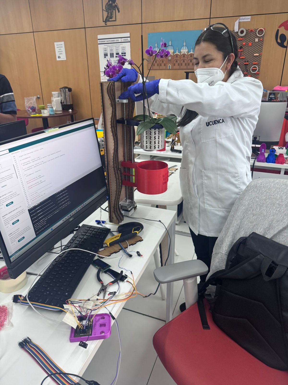
15. System Integration Testing
After placing the PCB, A4988 driver and wiring inside the printed PLA enclosure, I performed an integration testing process to verify that the electronic module could work as part of the complete OrquiWall Smart System. The purpose of this test was not only to check each component separately, but also to confirm that the mechanical, electronic, sensor, actuator, interface and packaging elements could work together as one system.
| Test | Objective | Procedure | Result |
|---|---|---|---|
| PCB fit test | Verify that the final project PCB fits inside the printed enclosure. | The PCB was placed inside the PLA base to check the available space, connector access and alignment. | The PCB fitted inside the enclosure and remained accessible for inspection and wiring. |
| A4988 driver placement test | Check that the motor driver has a dedicated position inside the case. | The A4988 driver was positioned in the lower internal area with its cables connected. | The driver could be placed inside the enclosure while keeping the wiring visible and accessible. |
| Cable routing test | Verify that the cables can exit the case without being compressed by the cover. | The sensor, motor and driver wires were routed through the side openings of the case. | The cables exited correctly through the designed openings and the cover could still be positioned. |
| Cover alignment test | Check if the removable cover aligns with the base after placing the electronics. | The cover was placed over the base with the PCB and cables inside. | The cover aligned with the base while leaving the cable path free. |
| Sensor connection test | Verify that the humidity sensor connection remains stable during handling. | The sensor cable was connected to the PCB and moved slightly to check if the connection remained in place. | The sensor connection remained connected and was not forced by the enclosure. |
| System status display test | Check that the display can show the main system states. | The system was programmed to show states such as dry substrate, wet substrate, moving up, irrigating and moving down. | The display identified the current operation state during the working system test. |
| Motor movement test | Verify that the stepper motor can move the reservoir using the lead screw mechanism. | The motor was activated through the A4988 driver to move the reservoir upward and downward. | The stepper motor moved the reservoir vertically as part of the irrigation sequence. |
| Limit switch test | Check that the upper and lower limit switches stop the motion safely. | The reservoir movement was tested until reaching the upper and lower limit switches. | The limit switches stopped the system at the upper and lower positions. |
| Complete cycle test | Evaluate the complete irrigation logic of the integrated system. | The complete cycle was tested: read humidity, move reservoir up, stop, irrigate by immersion, move reservoir down and stop. | The complete OrquiWall Smart System worked as an integrated prototype for automated orchid immersion irrigation. |
Testing conclusion: The integration test confirmed that the PCB, A4988 driver, sensor wiring and PLA enclosure work together as an organized electronic module. The complete system is already functioning as an integrated prototype: it reads the humidity condition, activates the motorized reservoir movement, stops with the limit switches, performs the immersion irrigation sequence and shows the operation status on the display.
16. Complete System Integration
After testing the electronic module, the OrquiWall Smart System was integrated as a complete final project prototype. The system includes the mechanical structure, the vertical movement mechanism, the custom PCB, the A4988 motor driver, the XIAO ESP32C3 microcontroller, the humidity sensor, the water/reservoir sensor, the display, the wiring and the PLA electronics enclosure.
The complete system is already working as an integrated prototype. The humidity sensor reads the orchid substrate condition, the PCB processes the input, the A4988 driver activates the stepper motor, and the reservoir moves vertically using the lead screw mechanism. The upper and lower limit switches stop the movement at the correct positions, and the display shows the system status during the process.
The purpose of this complete integration was to verify that the project works as a unified system instead of separate parts. The electronics were packaged inside the PLA case, the cables were routed through the designed exits, the sensor inputs were connected to the PCB, and the motor driver was connected to the stepper motor and limit switches.
The final working logic is: the system reads the humidity sensor, identifies if the orchid substrate is dry, activates the stepper motor, moves the reservoir upward, stops with the upper limit switch, performs the immersion irrigation stage, moves the reservoir downward, stops with the lower limit switch and updates the display status during the process.
Quantitative Sensor Measurement and Output Activation Logic
The final integration uses the output-device logic developed in Week 10. In the Arduino IDE code, the
humidity sensor is read with analogRead(SENSOR_PIN) and the value is printed in the Serial
Monitor as Humedad. The system uses a threshold value of 3000 to decide
when the orchid substrate is dry enough to activate the irrigation movement.
| Parameter from IDE Code | Quantitative Value | Function in the Integrated System |
|---|---|---|
| Sensor input pin | SENSOR_PIN = 2 |
The XIAO ESP32C3 reads the analog humidity sensor signal from this pin. |
| Sensor reading command | analogRead(SENSOR_PIN) |
The microcontroller converts the sensor signal into a numeric value for decision making. |
| Decision threshold | umbral = 3000 |
Values below this threshold are interpreted as dry substrate and start the irrigation sequence. |
| Measurement interval | delay(3000) = 3 s |
When the system is not busy, the sensor is checked approximately every 3 seconds. |
| Stepper pulse speed | velocidad = 900 us |
Each step pulse uses 900 us HIGH and 900 us LOW, producing approximately 556 pulses per second. |
| Up movement time | tiempoSubida = 3000 ms |
The reservoir moves upward for 3 seconds when irrigation starts. |
| Irrigation pause | delay(1000) = 1 s |
The system stays in the upper position for a short irrigation/immersion stage. |
| Down movement time | tiempoBajada = 3000 ms |
The reservoir moves downward for 3 seconds after irrigation. |
| Recovery time after irrigation | delay(6000) = 6 s |
The system waits before measuring humidity again to avoid repeating the cycle immediately. |
Sensor Data Interpretation
| Sensor Value Range | Condition Interpreted by the Code | Output Response | Serial Monitor Message |
|---|---|---|---|
humedad < 3000 |
Dry substrate | The irrigation movement sequence is activated. | SECO -> INICIANDO RIEGO |
humedad >= 3000 |
Humid enough / no irrigation needed | The motor remains stopped and the system continues monitoring. | Only the humidity value is printed. |
How Components Are Activated from Sensor Data
First, the XIAO ESP32C3 reads the humidity sensor. If the value is lower than 3000,
the variable sistemaOcupado changes to true. This prevents the controller
from taking new measurements while the reservoir is moving.
Input Devices Test Results Used for Integration
The following values come from the Week 09 Input Devices test, where the humidity sensor was read in the Arduino IDE Serial Monitor. In that test, all readings were classified as SUSTRATO HUMEDO. These results are useful for the system integration stage because they show the real sensor range observed when the substrate has enough moisture.
| No. | Humidity Sensor Value | Status Printed in Serial Monitor | Integration Meaning |
|---|---|---|---|
| 1 | 1093 | SUSTRATO HUMEDO | The substrate contains moisture, so irrigation should not be activated after calibration. |
| 2 | 1203 | SUSTRATO HUMEDO | The sensor detects a humid condition. |
| 3 | 1202 | SUSTRATO HUMEDO | The reading remains in the wet range. |
| 4 | 1113 | SUSTRATO HUMEDO | The substrate is still classified as wet. |
| 5 | 1216 | SUSTRATO HUMEDO | The analog value confirms humidity presence. |
| 6 | 1191 | SUSTRATO HUMEDO | The sensor response is stable. |
| 7 | 1220 | SUSTRATO HUMEDO | The substrate remains humid. |
| 8 | 1160 | SUSTRATO HUMEDO | The reading is consistent with previous values. |
| 9 | 1075 | SUSTRATO HUMEDO | The value is lower but still in the humid range. |
| 10 | 1039 | SUSTRATO HUMEDO | The substrate is still detected as wet. |
| 11 | 1041 | SUSTRATO HUMEDO | The reading confirms the humid condition. |
| 12 | 1015 | SUSTRATO HUMEDO | The reading remains in the wet range. |
| 13 | 1020 | SUSTRATO HUMEDO | The final value confirms the same humid condition. |
| Parameter | Result | Use in System Integration |
|---|---|---|
| Minimum observed value | 1015 | Lowest humid-substrate reading recorded during the input test. |
| Maximum observed value | 1220 | Highest humid-substrate reading recorded during the input test. |
| Approximate average value | 1122 | Reference value for a stable humid substrate condition. |
| Observed condition | SUSTRATO HUMEDO | The integrated system should keep the irrigation mechanism inactive when this condition is detected. |
Calibration note: the Week 09 sensor test shows that values around 1015 to 1220 correspond to SUSTRATO HUMEDO. Therefore, during final integration, the activation threshold must be calibrated so this humid range keeps the motor stopped, and only a dry-substrate range activates the irrigation movement.
For the upward movement, the program sets DIR_PIN to HIGH and sends pulses
through STEP_PIN for 3000 ms. The motor driver translates those pulses
into stepper motor movement, lifting the reservoir. Then the system waits 1000 ms
during the irrigation/immersion stage. For the downward movement, DIR_PIN changes to
LOW and the same pulse sequence is repeated for 3000 ms, lowering the
reservoir again.
Integration result: the sensor value controls the output behavior. A dry reading
(humedad < 3000) activates the electromechanical irrigation sequence, while a humid
reading keeps the mechanism stopped. This connects the input data, the IDE logic, the motor driver
and the physical reservoir movement into one automated system.
Final Assembly Design Adjustments
During the final assembly, I had to make some design adjustments to improve the integration of the complete OrquiWall Smart System. These adjustments were necessary because the real position of the PCB, A4988 driver, wiring, sensor cables and mechanical structure showed small differences compared with the initial CAD planning.
The main adjustments were related to cable routing, internal space, component placement and the way the electronics enclosure connected with the rest of the system. I verified that the cables could exit the case without being compressed, that the driver remained accessible, and that the electronic module could be placed safely during the final working test.
These changes helped transform the prototype from a set of designed parts into a functional integrated system. After the adjustments, the final assembly worked correctly: the system read the humidity condition, activated the motorized movement, stopped with the limit switches and performed the immersion irrigation sequence.
| Integrated Part | Final Working Evidence |
|---|---|
| Mechanical structure | The MDF wall frame and 3D printed supports hold the orchid, reservoir and movement mechanism in place. |
| Motion mechanism | The stepper motor, lead screw, guide system and limit switches allow the reservoir to move up and down during the irrigation cycle. |
| Electronic control | The custom PCB with the XIAO ESP32C3 reads the sensor input and controls the irrigation sequence. |
| Motor control | The A4988 driver receives signals from the PCB and controls the stepper motor movement. |
| Sensor inputs | The humidity sensor detects the substrate condition and the water/reservoir sensor supports the irrigation control. |
| User interface | The display shows the current state of the working system, including humidity condition and movement status. |
| Packaging | The PLA case protects the electronics and keeps the PCB, driver and wiring organized during system operation. |
| Final assembly adjustments | Some design adjustments were made during the final assembly to improve cable routing, component placement, enclosure fit and the connection between the electronics and the mechanical structure. |
| Complete system | The complete OrquiWall Smart System works as an integrated prototype for automated orchid immersion irrigation. |
Complete integration conclusion: The final project is already working as a complete integrated system. The mechanical structure, electronics, sensors, actuator, display, wiring and packaging work together to perform the automated orchid immersion irrigation cycle. This confirms that the project is more than a set of independent tests and that the main subsystems were integrated into one functional final prototype.
17. Download Files
The following files include the Fusion 360 design and exported fabrication files used for the system integration case. This documentation is also connected to the complete Final Project page, where the full prototype context can be reviewed.
18. Learning Outcomes
Through this integration task, I learned how to:
- Define and apply system integration to my final project.
- Design an enclosure based on the real needs of an electronic system.
- Plan internal space for a PCB, A4988 driver and cable routing.
- Track the progress of the final project by separating it into subsystems.
- Identify the origin and availability of the main materials and components.
- Create a two-part case in Fusion 360 using sketches, extrusions and rounded corners.
- Prepare a PLA print in Bambu Studio for the Bambu Lab printer.
- Use 3D printing as a system integration tool, not only as an isolated fabrication process.
- Test the integrated system by checking the PCB fit, cable routing, sensor connection and motion sequence.
- Document the final project as a complete integrated system, not only as separated components.
- Adjust the design during final assembly according to the real behavior of the prototype.
- Evaluate the case as a prototype that can be improved after final wiring tests.
19. Final Reflection
This week connected the electronic work of the final project with a physical enclosure. Designing the PCB is not enough for the final system; the components also need to be protected, positioned and connected in a controlled way. The PLA case helps transform the electronics from a test setup into a more integrated module.
I also improved my project planning by tracking the progress of the main subsystems and identifying which parts were completed, which parts were still in progress, and which actions were required for the next tests. This helped me understand the final project as a complete system instead of isolated weekly assignments.
The country of origin and sourcing table helped me identify which components were fabricated locally and which ones depended on external suppliers. This is useful for future improvements because it shows where the project can become more locally manufacturable and where replacement components may be needed.
The system integration testing helped me verify that the PCB, A4988 driver, wiring and PLA enclosure can work together as one organized electronic module. The testing also confirmed that the system can read the sensor input, activate the motor movement and stop using the limit switches.
The complete OrquiWall Smart System is already functioning as an integrated prototype. The system can read the humidity condition, activate the motorized reservoir movement, stop using the limit switches, perform the immersion irrigation sequence and show the operation status on the display.
During the final assembly, I also learned that the CAD design must be adjusted according to the real behavior of the physical prototype. Some modifications were necessary to improve the enclosure fit, cable routing, component placement and connection between the electronic module and the mechanical structure. These adjustments helped the system work correctly as a final integrated prototype.
The case still has room for iteration, especially after testing repeated cycles with the A4988 driver and final project PCB. However, this prototype already defines the size, structure and cable organization needed for the working final project.
To review the complete context of the project, including the final system design, fabrication, electronics, testing and final result, please visit my Final Project page.
20. System Architecture Overview
As a final visual summary of the system integration process, I created an architecture and components overview for the Smart Orchid Immersion Irrigation System. The image organizes the final project into structural components, irrigation module, mechanical system, electronic system, power system, assembled modules and key features.
This diagram helps explain how the complete prototype is not a single isolated mechanism, but a complete integration of fabricated parts, electronics, sensing, motion control, power regulation and assembled modules working together.
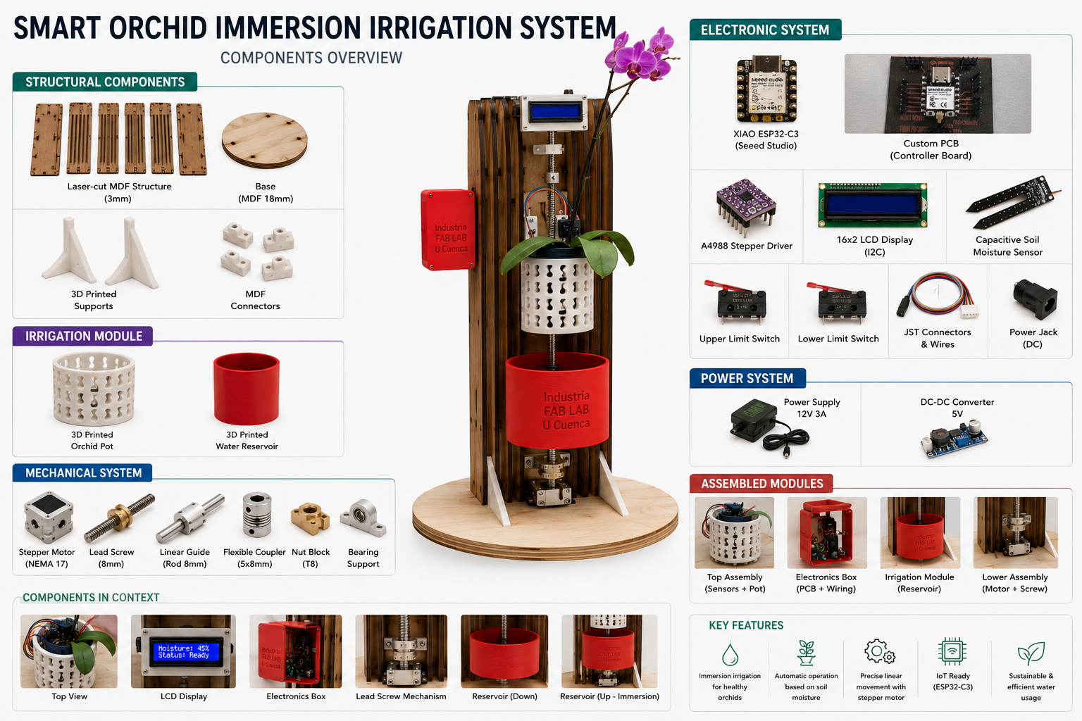
| System Area | Parts Included | Integration Role |
|---|---|---|
| Structural components | Laser-cut MDF structure, base, 3D printed supports and MDF connectors. | Provides the physical frame that holds the orchid, reservoir, electronics and movement mechanism. |
| Irrigation module | 3D printed orchid pot and 3D printed water reservoir. | Allows the orchid pot to be immersed in water during the automatic irrigation cycle. |
| Mechanical system | NEMA 17 stepper motor, lead screw, linear guide, coupler, nut block and bearing support. | Creates the vertical movement needed to raise and lower the reservoir. |
| Electronic system | XIAO ESP32-C3, custom PCB, A4988 driver, LCD display, capacitive soil moisture sensor, limit switches, JST connectors and power jack. | Reads the sensors, controls movement, displays status and manages the system logic. |
| Power system | 12 V 3 A power supply and 5 V DC-DC converter. | Supplies the motor driver and regulates power for the electronic control system. |
| Assembled modules | Top assembly, electronics box, irrigation module and lower assembly. | Shows how individual fabricated and electronic parts become functional subsystems. |
Prompt Used as Evidence
Create a clean technical infographic titled "Smart Orchid Immersion Irrigation System - Components Overview".
Use the OrquiWall orchid irrigation prototype as the central object. Show the assembled system in the center
with the orchid pot, vertical wooden structure, electronics box, LCD display, lead screw mechanism and red
water reservoir. Around the central prototype, organize the components into labeled sections:
Structural Components, Irrigation Module, Mechanical System, Electronic System, Power System, Assembled Modules
and Key Features. Include visual references for the laser-cut MDF structure, MDF base, 3D printed supports,
orchid pot, water reservoir, NEMA 17 stepper motor, lead screw, linear guide, coupler, nut block, bearing support,
XIAO ESP32-C3, custom PCB, A4988 driver, 16x2 I2C LCD display, capacitive soil moisture sensor, upper and lower
limit switches, JST connectors, wires, DC power jack, 12 V power supply and 5 V DC-DC converter. Use a clear
white background, technical labels, organized boxes and a professional engineering documentation style.