WEEK 08 – Electronics Production
GROUP ASSIGNMENT — Fiber Laser PCB Characterization
Group Objective
The group assignment focused on analyzing and characterizing the fabrication capabilities of a 50 W JPT fiber laser machine for PCB production. The main goal was to understand how different fabrication parameters affect the quality, precision, and reliability of PCB traces.
During this activity, the group evaluated the behavior of the fiber laser when engraving copper-clad boards. Parameters such as power, speed, frequency, focus, hatch spacing, and number of passes were considered in order to identify a suitable workflow for PCB manufacturing.
| Group Task | Description |
|---|---|
| Machine Characterization | Analyze the fiber laser performance for PCB fabrication. |
| Parameter Testing | Compare engraving results using different laser settings. |
| Trace Quality | Evaluate copper removal, trace definition, and isolation quality. |
| Fabrication Workflow | Define a reliable process for producing PCBs with the fiber laser. |
PCB Manufacturing with Fiber Laser
PCB fabrication in this assignment was developed using a fiber laser workflow. This process allowed direct copper engraving on the PCB surface and required careful adjustment of fabrication parameters to achieve clean trace isolation.
The fiber laser process was especially useful for fast experimentation and direct copper engraving. However, it required calibration to avoid burning the substrate, leaving copper residues, or damaging fine traces.
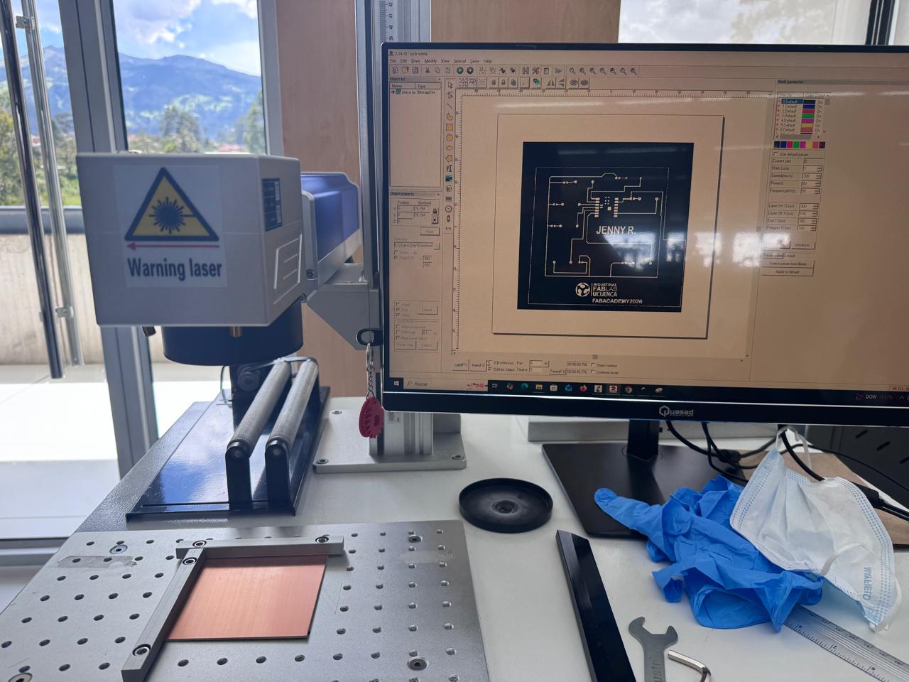
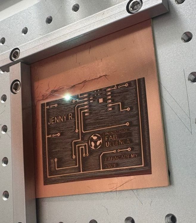
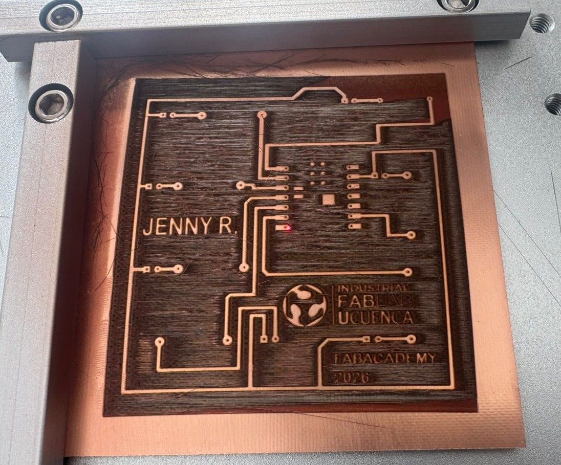
Group assignment evidence: PCB characterization and fabrication tests using fiber laser technology.
Machine Identification and Technical Specifications
To make the PCB fabrication process reproducible, the machine used during the electronics production workflow was identified from the nameplate attached to the laser source. The individual LED roulette PCB was fabricated using a JPT pulsed fiber laser source.
| Technical Specification | Value |
|---|---|
| Brand | JPT |
| Model | YDFLP-E-50-LP-L-R |
| Laser Type | Pulsed fiber laser, LP series |
| Nominal Average Output Power | > 50 W |
| Maximum Pulse Energy | 1.25 mJ |
| Pulse Repetition Rate Range | 1 – 600 kHz |
| Pulse Duration | 200 ns |
| Output Power Stability | < 5% |
| Cooling Method | Air cooled |
| Supply Voltage | 24 VDC |
| Maximum Power Consumption | < 220 W |
| Serial Number | MC2BCJC35960 |
| Part Number | 200101000018 |
| Production Date | 03/2023 |
| Country of Manufacture | Made in China |
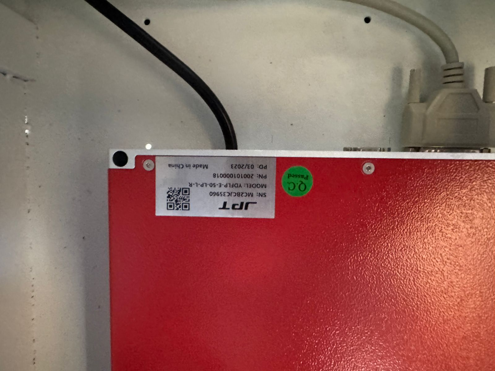
Nameplate of the JPT fiber laser source used for PCB production.
The PCB of this assignment was fabricated using the JPT YDFLP-E-50-LP-L-R pulsed fiber laser source. CNC milling references were removed from this page because the individual assignment documentation is focused only on the actual fabrication process used for this board.
Individual Assignment
LED Roulette PCB using XIAO ESP32-C3
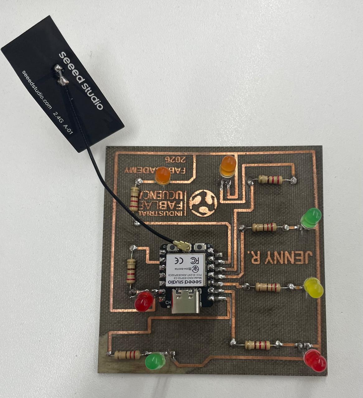
This assignment focused on the complete workflow of electronics production, including PCB design, fabrication, drilling, soldering, programming, and functional validation. The project consisted of developing a custom PCB for a LED roulette system controlled by a Seeed Studio XIAO ESP32-C3.
The roulette system was designed using seven LEDs connected to independent GPIO pins of the XIAO ESP32-C3. Each LED includes a 220 Ω resistor to protect both the LED and the microcontroller from excessive current.
The PCB was designed in KiCad, fabricated using a JPT fiber laser engraver, manually soldered, and programmed using Arduino IDE to generate the roulette animation effect.
PCB Design Process in KiCad
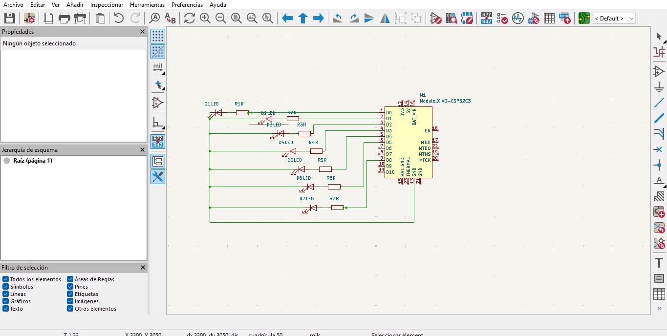
The PCB design started in KiCad by creating the schematic for a LED roulette controlled by the XIAO ESP32-C3. Seven LEDs were connected to independent GPIO pins, and each LED was paired with a current-limiting resistor to protect the components during operation.
After checking the schematic connections, the project was moved to the PCB editor. The XIAO ESP32-C3 footprint was placed in the center of the board, while the LEDs and resistors were distributed around it to keep the circuit readable and to support the roulette animation.
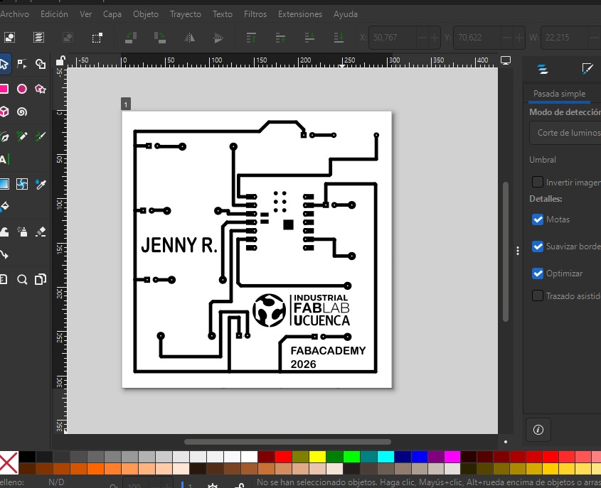
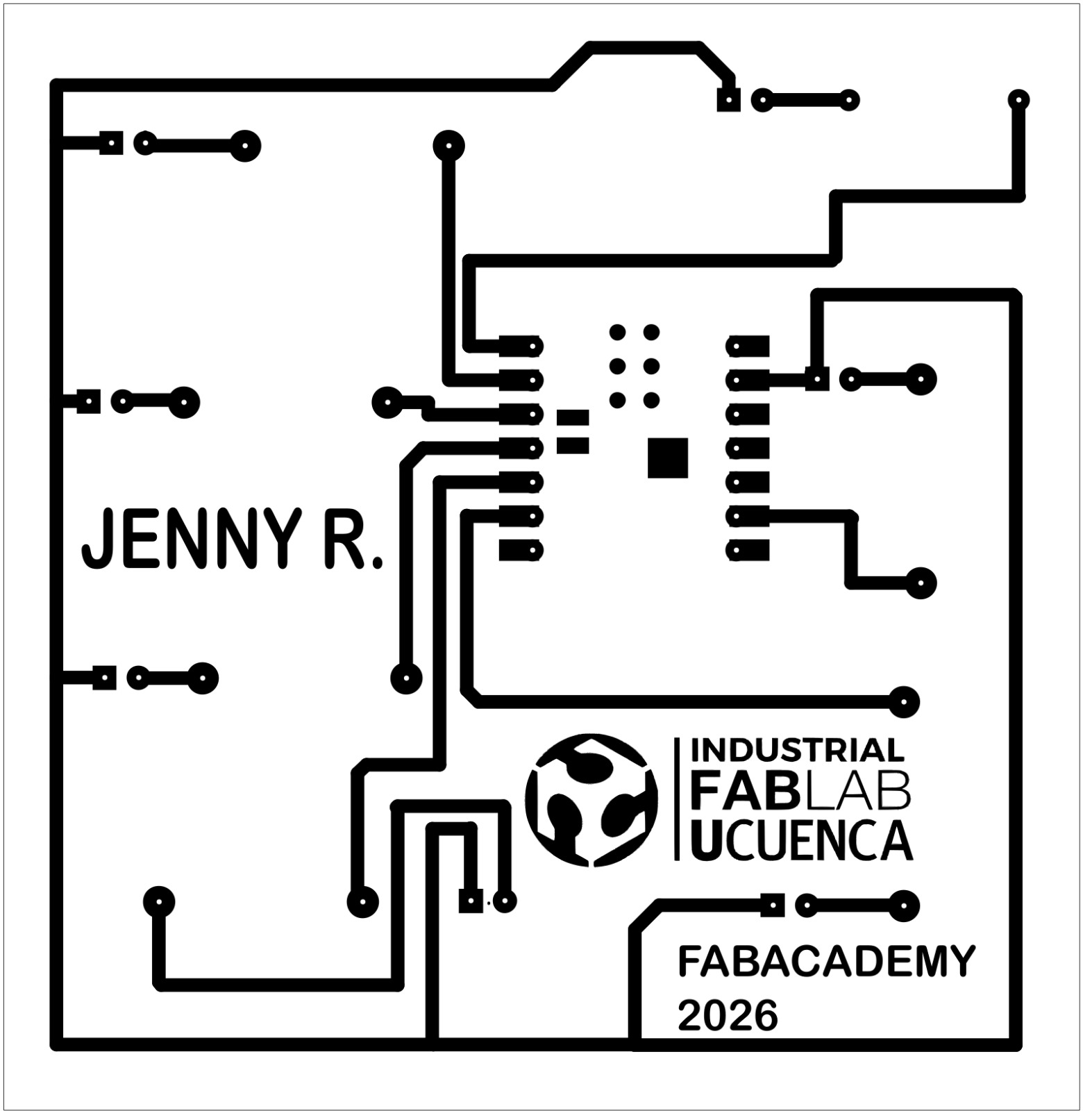
The traces were routed on the front copper layer, maintaining clear spacing between tracks and pads so the design could be manufactured with the fiber laser process. The board outline was then defined on the Edge.Cuts layer, and the trace artwork was exported for preparation in Inkscape.

1. Assignment Objective
Main Objective
The main objective of this assignment was to explore the complete workflow of electronics production through the development of a functional LED roulette PCB. This process included electronic design, PCB layout generation, fabrication, drilling, soldering, programming, and final validation of the circuit.
In addition, this assignment reinforced the relationship between digital design and physical manufacturing processes. Understanding how traces, pads, and component placement influence fabrication quality was essential to achieve a reliable and operational electronic board.
| Objective | Description |
|---|---|
| Electronic Design | Create the schematic and PCB layout in KiCad. |
| PCB Fabrication | Fabricate the PCB using a fiber laser engraving process. |
| Assembly | Solder and assemble the electronic components. |
| Programming | Program the XIAO ESP32-C3 using Arduino IDE. |
| Validation | Verify correct operation of the LED roulette sequence. |
2. Components Used
The electronic system was designed around the Seeed Studio XIAO ESP32-C3, a compact microcontroller board with integrated WiFi and BLE connectivity. This board was selected because of its small size, processing capabilities, and sufficient GPIO pins for controlling multiple LEDs independently.
The circuit also included seven LEDs and seven 220 Ω resistors. Each resistor was connected in series with an LED to limit electrical current and protect both the LEDs and the microcontroller pins from excessive power consumption.
Additional materials such as a copper-clad PCB, solder wire, and header pins were used during the fabrication and assembly stages of the assignment.
| Component | Quantity | Function |
|---|---|---|
| Seeed Studio XIAO ESP32-C3 | 1 | Main controller of the LED roulette system. |
| LEDs | 7 | Visual outputs used to create the roulette animation. |
| 220 Ω Resistors | 7 | Current-limiting resistors connected in series with each LED. |
| Copper PCB Board | 1 | Base material used for PCB fabrication. |
| Header Pins | As needed | Used to mount and connect the XIAO ESP32-C3. |
3. PCB Design in KiCad
The PCB design process started in KiCad, an open-source electronic design software widely used for schematic creation and PCB layout development. During this stage, the complete electronic circuit was organized digitally before fabrication.
Each GPIO pin of the XIAO ESP32-C3 was assigned to one LED through a current-limiting resistor. The schematic allowed verification of all electrical connections and ensured that the board would operate correctly before continuing with the manufacturing process.
Schematic Design Process
- Create a new KiCad project.
- Add the XIAO ESP32-C3 symbol.
- Add seven LEDs and seven 220 Ω resistors.
- Connect each LED-resistor pair to a GPIO pin.
- Connect all LED cathodes to GND.
- Run the Electrical Rules Check.
- Correct warnings before moving to PCB layout.
KiCad schematic of the LED roulette circuit.
4. ERC and DRC Verification
Before fabrication, the design was verified using KiCad checks. The Electrical Rules Check was used to validate the schematic connections, while the Design Rules Check was used to confirm that the PCB layout respected the required trace width, spacing, and clearance for the selected fabrication process.
| Check | Software | Purpose | Result |
|---|---|---|---|
| ERC – Electrical Rules Check | KiCad Schematic Editor | Verify electrical connections, power pins, and unconnected nets | No critical errors after review |
| DRC – Design Rules Check | KiCad PCB Editor | Verify track width, clearance, pads, and board outline | No critical errors after review |
These checks were important because fabrication errors in electronics production can lead to open circuits, short circuits, or components that cannot be soldered correctly. After completing ERC and DRC verification, the design was considered ready for export and fabrication.
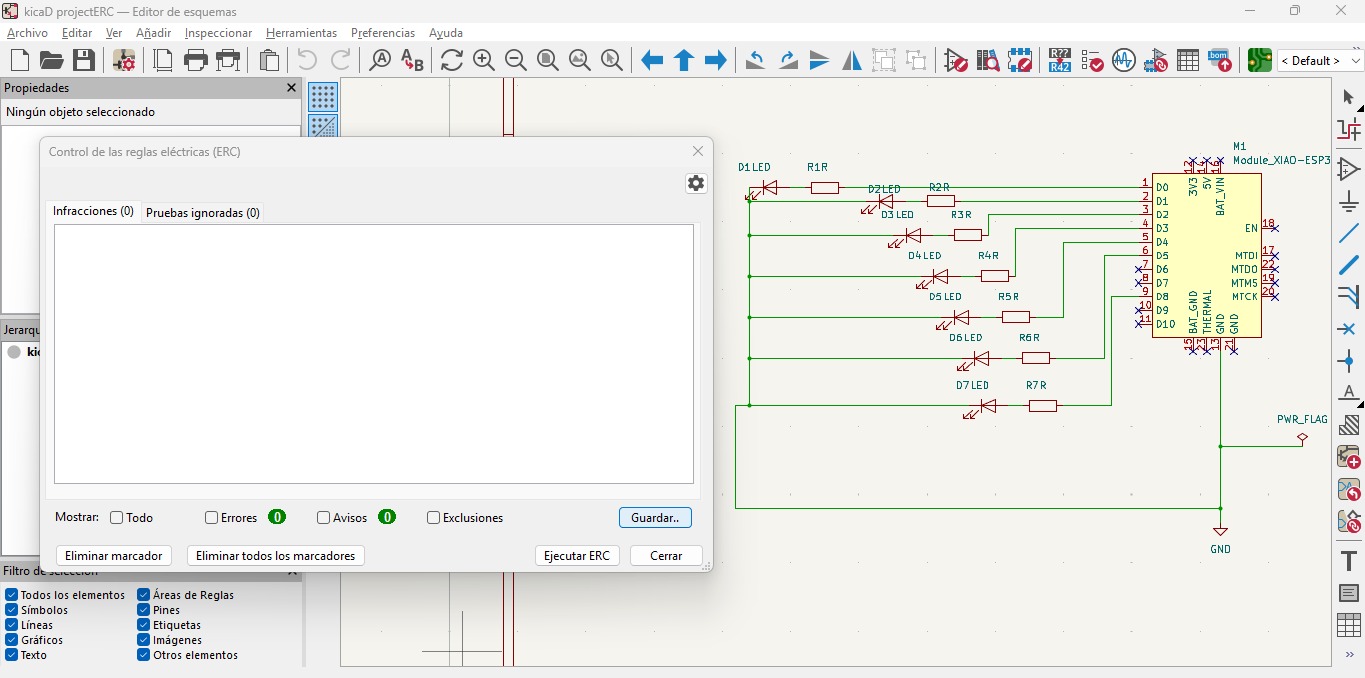
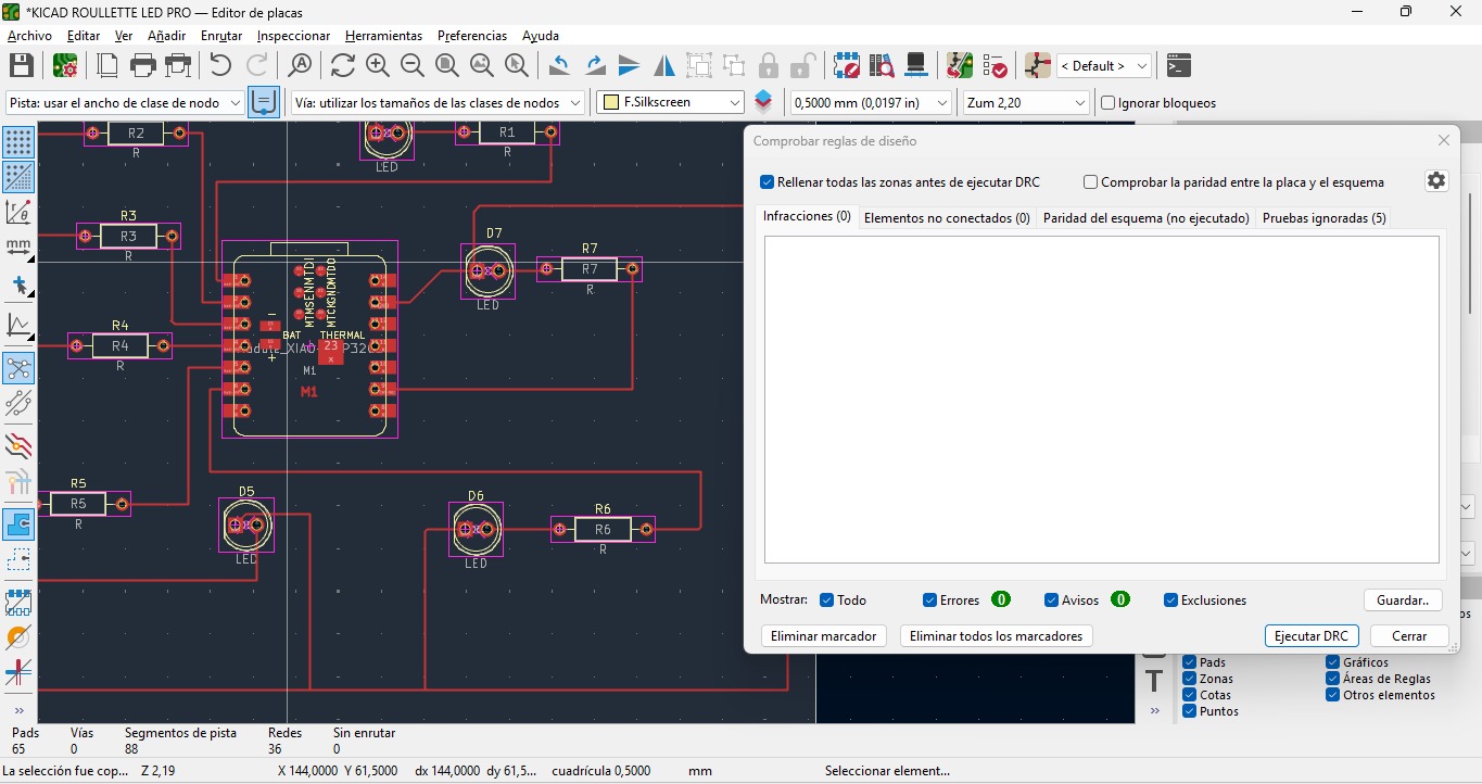
The ERC and DRC screenshots were captured from KiCad after checking the schematic and PCB layout. No critical errors remained before fabrication.
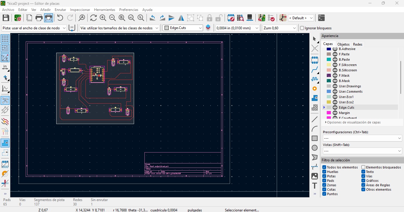
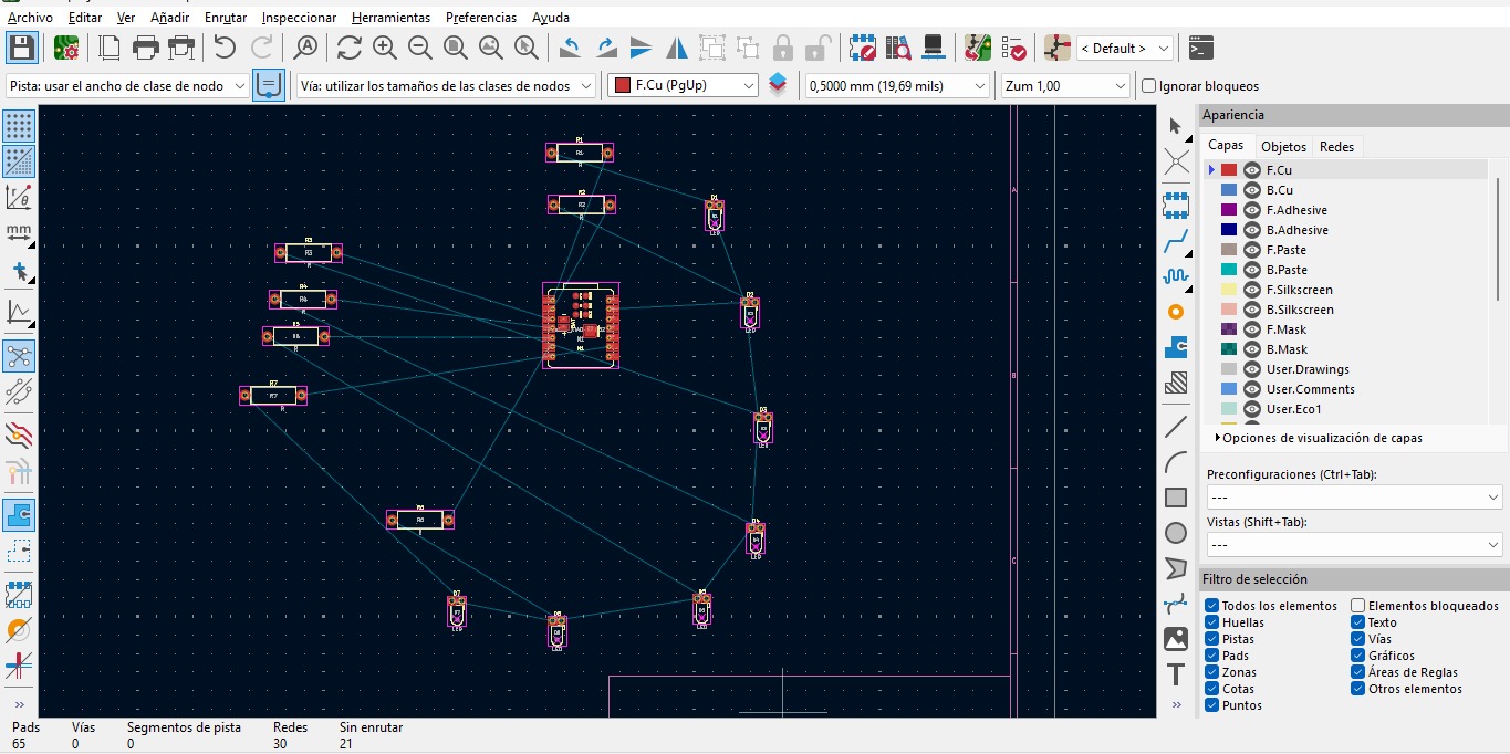
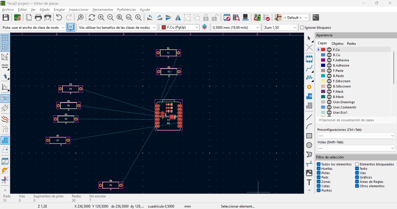
5. PCB Layout Design
After completing the schematic, the project was transferred to the PCB editor in KiCad to begin the physical layout design. This stage involved organizing the position of all electronic components and routing the copper traces that electrically connect the circuit.
The LEDs were arranged in a roulette-style distribution to create a dynamic visual effect during operation. The XIAO ESP32-C3 was positioned to allow easy USB access for programming and testing.
For this board, the main traces were designed using a minimum trace width of approximately 0.40 mm and a minimum spacing of approximately 0.20 mm. These values were selected based on the fiber laser characterization tests and the expected fabrication capability of the process.
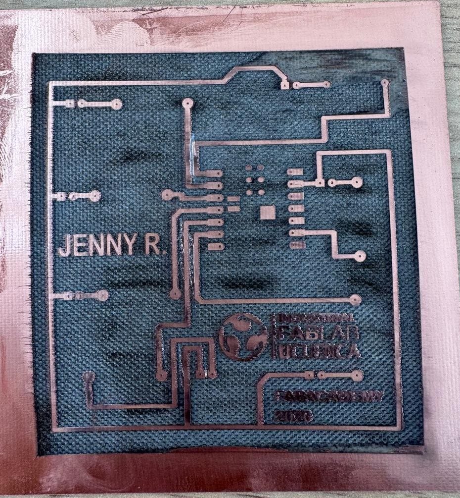
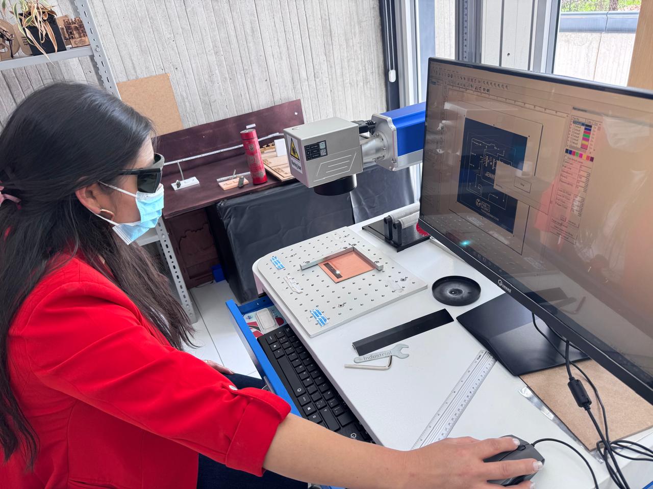
6. PCB Fabrication with Fiber Laser
Once the PCB design was completed, the fabrication process was performed using a JPT YDFLP-E-50-LP-L-R pulsed fiber laser source. The laser engraving method allowed direct copper removal on the PCB surface with high precision.
During this process, parameters such as power, speed, frequency, hatch spacing, number of passes, and focus were adjusted carefully to achieve clean traces without damaging the board.
Exact Laser Parameters Used During Fabrication
The following table summarizes the machine configuration and the fabrication parameters used during the PCB engraving process. These values define the operating conditions used to remove copper and produce the final board.
| Laser Parameter | Exact Value Used |
|---|---|
| Machine Brand | JPT |
| Machine Model | YDFLP-E-50-LP-L-R |
| Laser Type | Pulsed fiber laser |
| Nominal Output Power | > 50 W |
| Working Lens / Head Diameter | 100 mm |
| Distance from Laser Head to Material | 190 mm |
| Material | Copper-clad PCB substrate |
| Operation | Copper isolation / PCB engraving |
| Power Setting | 70% |
| Speed | 1000 mm/s |
| Frequency | 30 kHz |
| Hatch Spacing | 0.03 mm |
| Number of Passes | 4 passes |
| Focus | Manual focus adjusted on the copper surface before engraving |
These parameters were selected because they provided enough energy to remove copper while reducing the risk of burning the substrate or damaging thin PCB traces.
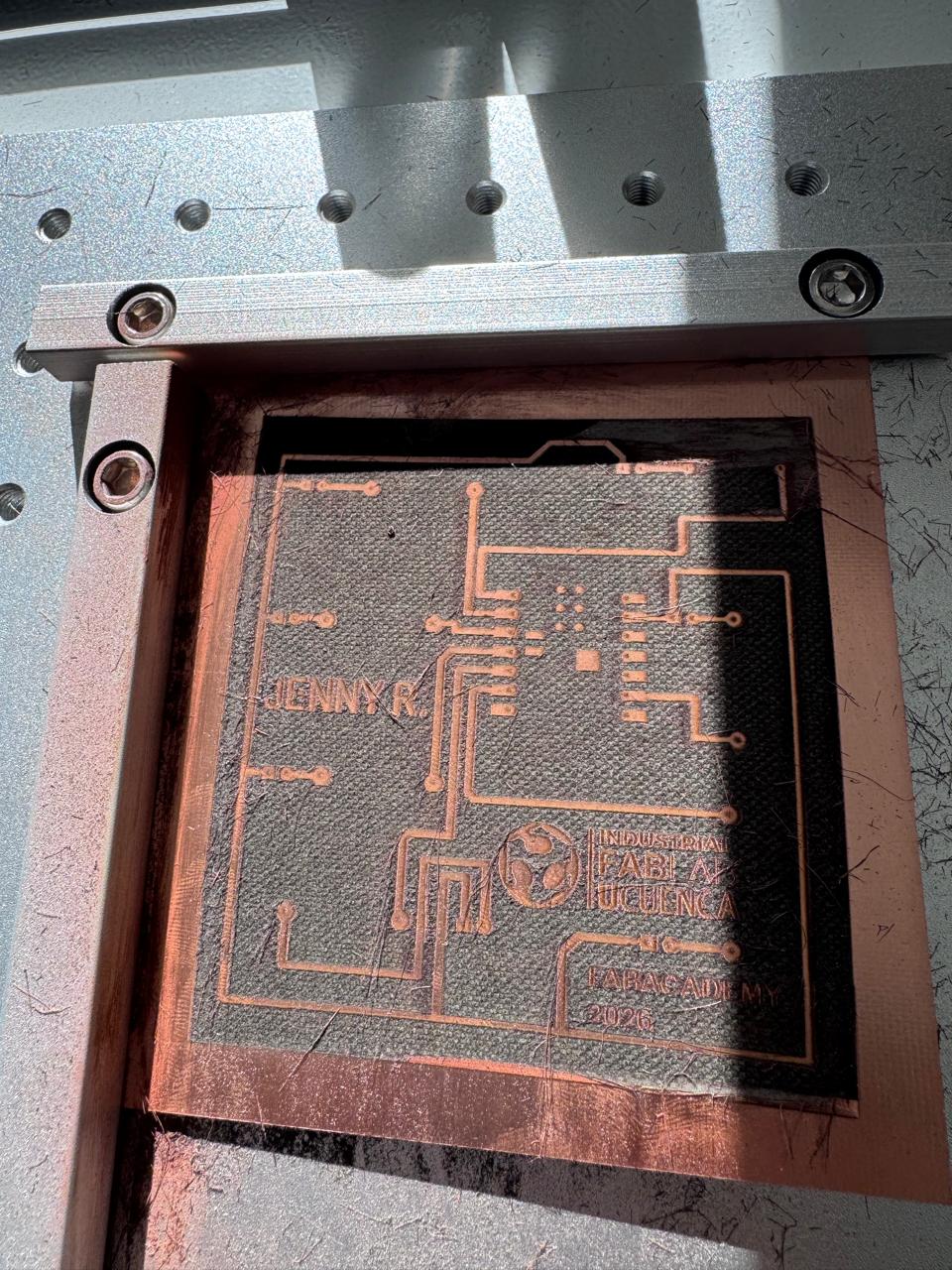
7. Measured Fabrication Capabilities
The following table presents the measured fabrication capabilities obtained from the PCB production process. These values represent the minimum reliable features that could be fabricated and maintained after engraving and cleaning.
| Capability | Measured Result |
|---|---|
| Minimum Trace Width | 0.40 mm |
| Minimum Spacing | 0.20 mm |
| Material Removal Method | Laser ablation of copper |
| Main Limitation | Risk of incomplete copper removal or substrate burning if parameters are not calibrated correctly |
| Best Use Case | Fast PCB prototyping with fine detail and direct copper isolation |
Based on these results, the fiber laser process was able to produce reliable PCB traces with a minimum trace width of 0.40 mm and a minimum spacing of 0.20 mm. These measurements were useful for defining the design limits that should be respected in KiCad before fabrication.
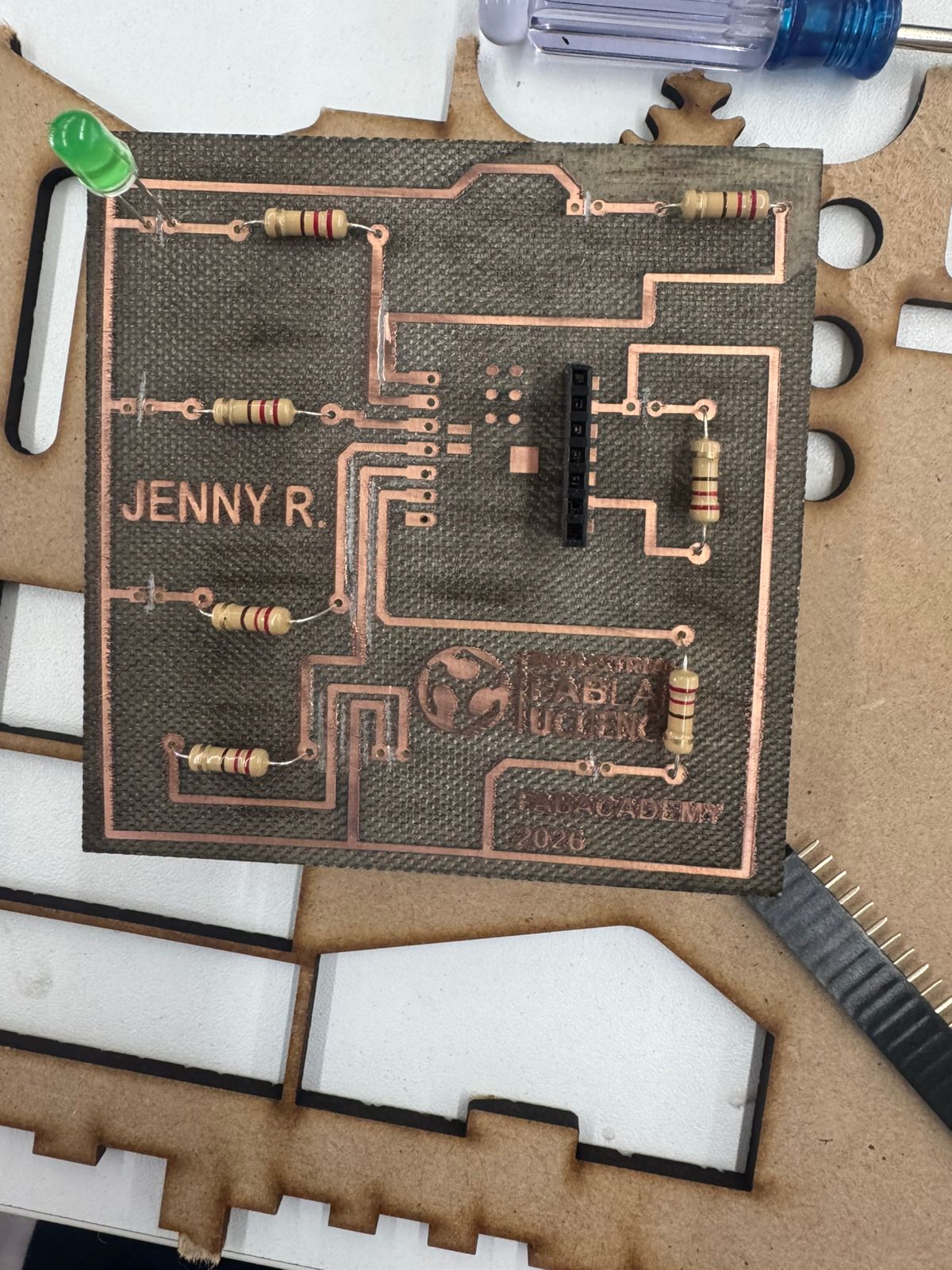
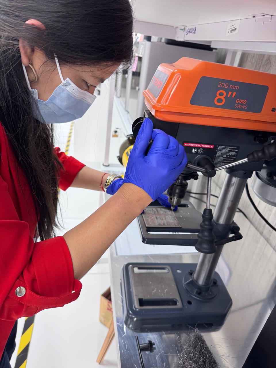
8. Drilling and Cleaning
After the engraving process was completed, the PCB required drilling operations to prepare the holes for electronic components and header connections.
Once drilling was completed, the PCB was cleaned to remove copper particles, dust, and fabrication residues that could generate short circuits.
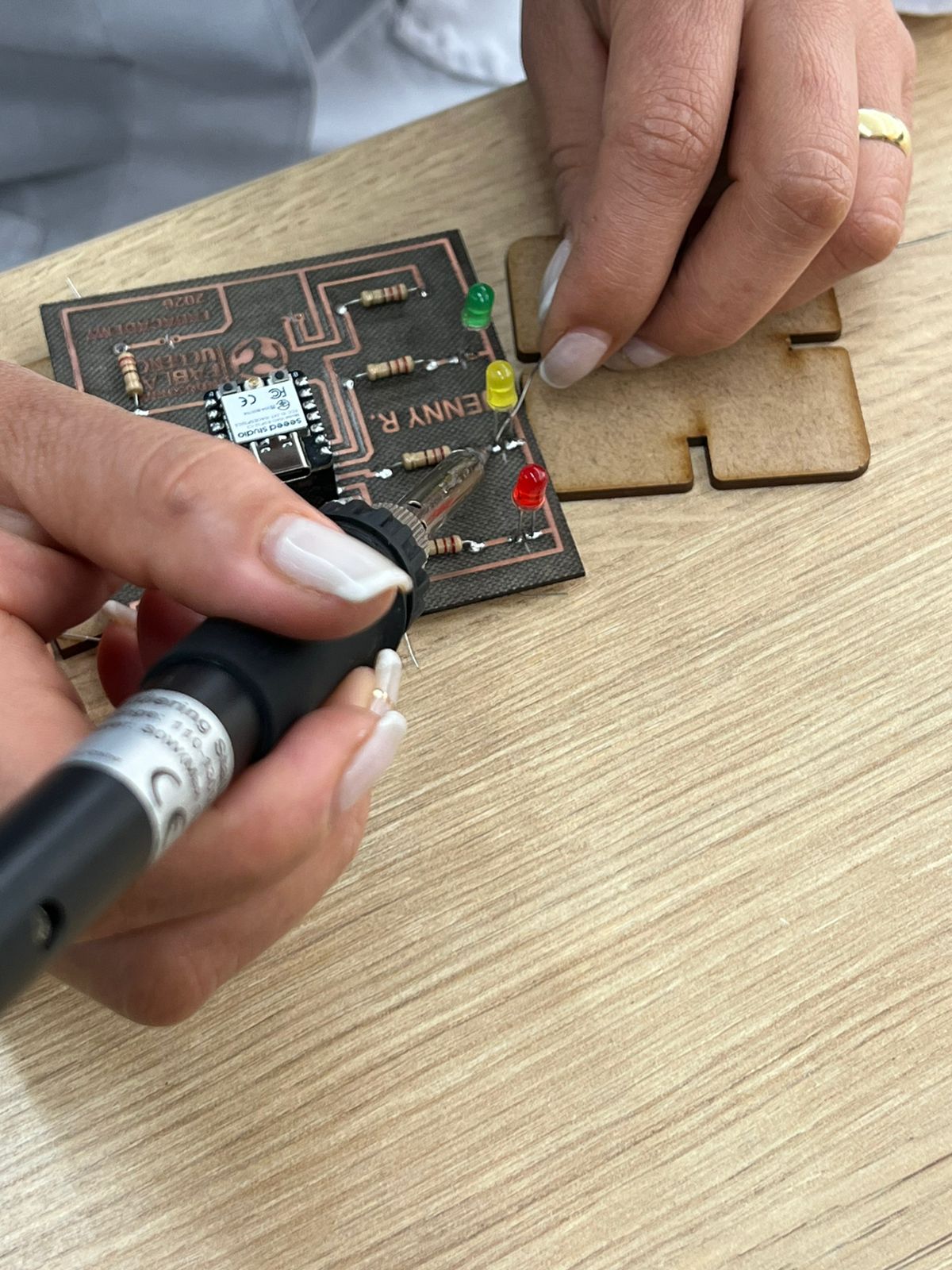
9. Soldering Process
The soldering stage consisted of assembling all electronic components onto the fabricated PCB. Manual soldering was used to connect the resistors, LEDs, header pins, and the XIAO ESP32-C3 to the board.
Special attention was given to LED polarity, solder quality, and avoiding solder bridges between adjacent pads.
10. Programming the LED Roulette
After completing the electronic assembly, the XIAO ESP32-C3 was programmed using Arduino IDE. The program generates a sequential LED animation capable of simulating the visual effect of a roulette.
int ledPins[] = {2, 3, 4, 5, 6, 7, 8};
int numberOfLeds = 7;
void setup() {
for (int i = 0; i < numberOfLeds; i++) {
pinMode(ledPins[i], OUTPUT);
digitalWrite(ledPins[i], LOW);
}
}
void loop() {
for (int i = 0; i < numberOfLeds; i++) {
digitalWrite(ledPins[i], HIGH);
delay(120);
digitalWrite(ledPins[i], LOW);
}
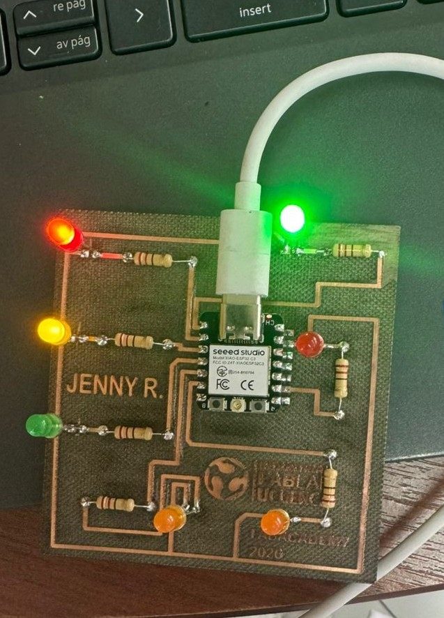
}11. Testing and Validation
Once the code was uploaded successfully, the PCB underwent a functional validation process. The LEDs responded correctly according to the programmed sequence, confirming successful fabrication and assembly.
12. Problems and Solutions
During the development process, different technical challenges appeared during fabrication, soldering, and programming. Solving these issues was an important part of the learning experience.
| Problem | Solution |
|---|---|
| Some LEDs did not turn on. | Verify polarity and solder joints. |
| Short circuit between traces. | Clean PCB and inspect solder bridges. |
| Laser engraving incomplete. | Adjust laser power, focus, hatch spacing, and number of passes. |
| Board not detected. | Check USB cable and Arduino IDE configuration. |
13. Download Files
The following files correspond to the design and fabrication resources developed during this assignment.
14. Final Conclusion and Reflection
This assignment allowed me to understand the complete workflow of electronics production, from digital design to fabrication and validation of a functional PCB. Through the development of the LED roulette project, I designed the circuit in KiCad, prepared the PCB layout, fabricated the board with a fiber laser machine, assembled the electronic components by soldering, programmed the XIAO ESP32-C3, and validated the final operation of the board.
One of the most important aspects of this assignment was understanding that PCB fabrication quality depends not only on the schematic design, but also on the real fabrication capability of the machine. For this reason, the ERC and DRC checks were essential before fabrication, since they helped verify that the circuit was electrically correct and that the layout respected the design rules needed for manufacturing.
The fiber laser fabrication process required careful control of the machine configuration and engraving parameters. In this case, the PCB was fabricated using a JPT YDFLP-E-50-LP-L-R pulsed fiber laser source with a 100 mm working lens/head diameter and a 190 mm distance from the laser head to the material. The engraving process was performed using 70% power, 1000 mm/s speed, 30 kHz frequency, 0.03 mm hatch spacing, and 4 passes. These parameters provided a useful balance between copper removal and trace preservation.
From a quantitative point of view, the measured fabrication results showed that the process was able to produce a minimum trace width of 0.40 mm and a minimum spacing of 0.20 mm. These values are important because they define the practical design limits that should be respected in future PCB layouts. If the traces are designed below these limits, the probability of fabrication failure increases.
Overall, this assignment strengthened my understanding of electronics production as a complete workflow where design, machine calibration, fabrication parameters, soldering quality, and functional validation are all interconnected. The final result was a functional LED roulette PCB, and the experience helped me better understand how to transform a digital electronic design into a real and working physical board.
Final Revision Checklist
- ✔ Machine brand and model identified: JPT YDFLP-E-50-LP-L-R.
- ✔ Laser type identified: pulsed fiber laser, LP series.
- ✔ Nominal output power included: > 50 W.
- ✔ Working lens / head diameter included: 100 mm.
- ✔ Distance from laser head to material included: 190 mm.
- ✔ Exact fabrication parameters added.
- ✔ Minimum trace width reported: 0.40 mm.
- ✔ Minimum spacing reported: 0.20 mm.
- ✔ ERC check added and documented.
- ✔ DRC check added and documented.
- ✔ Provisional notes removed.
- ✔ CNC references removed because no fabrication evidence was documented for this assignment.
- ✔ Final reflection improved with quantitative results.
- ✔ Download files verified.