Week 06-Electronics Design
Electronics Design · Fab Academy 2026 – Industrial FabLab UCuenca
Focus: schematic design, component selection, pin assignment, footprints, PCB layout, routing, design rules, fabrication check, and downloadable KiCad board files.
Group Assignment
For the group assignment, we reviewed the electronics design workflow as a lab team. We compared design rules, trace width, clearance, pad size, and the relationship between schematic decisions and PCB layout decisions. This group work helped me understand that the individual PCB should not be treated as a drawing only; every line, footprint, and connection must respond to an electrical function and to a clear design rule.
From the group activity, I used the idea of checking the board before routing: first defining the components, then assigning pins, then confirming footprints, and finally reviewing the board with the design rule check. That process became the base for my individual LED roulette PCB.
Individual Assignment Objective
In this assignment I designed a PCB in KiCad. My objective was to document the complete electronic design process: selecting the circuit, defining the controller pins, drawing the schematic, assigning footprints, placing the components, routing the board, reviewing the design rules, checking that the board could be fabricated, and preparing the design files for download.
This page intentionally focuses only on electronic design, so the documentation is centered on how the board was planned, drawn, routed, reviewed, and exported as original design files.
I designed this board from scratch in KiCad. I did not modify an existing EDA project. The schematic, footprint assignment, component placement, PCB routing, board outline, and final board layout were created as part of my individual electronics design workflow.
KiCad Workflow
I used KiCad as the main software for the complete electronics design workflow. The program allowed me to move from the schematic idea to the physical PCB layout using separated tools: schematic editor, symbol libraries, footprint editor, PCB editor, 3D viewer, and design verification tools. This separation helped me understand that electronic design is not a single drawing, but a sequence of connected decisions.
| KiCad Step | What I Did | Why It Was Important |
|---|---|---|
| 1. Project setup | I opened KiCad and organized the project files for the LED roulette board. | A clean project structure keeps schematic, PCB layout, and output files linked. |
| 2. Schematic editor | I placed the XIAO ESP32-C3, seven LEDs, and seven resistors. | The schematic defines the electrical logic of the board. |
| 3. Footprint assignment | I linked each schematic symbol to its physical footprint. | This step connects the electronic diagram with the real board geometry. |
| 4. PCB editor | I arranged components, followed the ratsnest, routed traces, and defined the board outline. | The PCB editor converts the circuit into a physical layout. |
| 5. ERC / DRC review | I checked schematic connections and board routing problems. | ERC and DRC helped me find missing nets, spacing issues, and incomplete routing. |
| 6. Fabrication check | I reviewed track width, clearance, pad spacing, and board outline before exporting. | This helped me confirm that the board could be fabricated and inspected clearly. |
| 7. 3D viewer | I inspected the assembled board virtually. | The 3D view helped confirm component orientation, spacing, and visual readability. |
| 8. Output files | I exported the final board artwork and downloadable KiCad files. | The final files document the board and allow the design to be reused or reviewed later. |
Board Concept
The board documented here is a LED roulette PCB controlled by a Seeed Studio XIAO ESP32-C3. I used this board as a learning platform because it is simple enough to understand clearly, but complete enough to practice the main stages of PCB design.
The circuit uses seven LEDs, seven 220 ohm current-limiting resistors, and header connections for the XIAO ESP32-C3. Each LED is connected to a different GPIO pin so the roulette sequence can be controlled independently in software.
Controller
Seeed Studio XIAO ESP32-C3 as the main microcontroller.
Output
Seven LEDs arranged for a roulette-style visual sequence.
Protection
One 220 ohm resistor in series with each LED.
Design Goal
Create a clean, readable, rule-checked, and fabricable PCB layout.
Interaction and Communication with the Microcontroller
This board was designed as a small development board around the Seeed Studio XIAO ESP32-C3. The local interaction with the embedded microcontroller is achieved through seven LEDs, which are controlled independently by GPIO pins. Each LED provides a visible output response, allowing me to test digital outputs and verify the behavior of the programmed sequence.
In addition to the local LED outputs, the board keeps the XIAO ESP32-C3 accessible as the embedded microcontroller module. The USB connector allows programming and serial communication with a computer, while the XIAO header pins make it possible to connect external devices or future input/output modules. This means the board can interact locally through the LEDs and communicate externally through the microcontroller communication interfaces.
| Requirement | How My Board Responds |
|---|---|
| Local interaction | The seven LEDs are controlled by GPIO pins and provide visual feedback from the microcontroller. |
| Embedded microcontroller | The board uses the Seeed Studio XIAO ESP32-C3 as the main embedded controller. |
| External communication | The XIAO ESP32-C3 can communicate with a computer through USB serial and can connect to external devices using its available GPIO and communication pins. |
| Development board function | The board can be programmed, tested with local outputs, and expanded for future external devices. |
Design Requirements
Before drawing the schematic, I defined the board requirements. This helped me keep the design organized and made the transition from schematic to PCB layout more controlled.
| Requirement | Design Decision | Reason |
|---|---|---|
| Use a compact controller | XIAO ESP32-C3 footprint placed as the central component. | The board remains small and the USB connector can stay accessible. |
| Control several outputs | Seven GPIO pins assigned to seven LEDs. | The roulette sequence requires independent LED control. |
| Protect the LEDs | One 220 ohm resistor placed in series with each LED. | The resistor limits current and protects the LED and GPIO pin. |
| Allow communication | The XIAO ESP32-C3 remains accessible through USB and header pins. | The board can communicate with a computer and can be expanded with external devices. |
| Keep the layout readable | Components placed with clear spacing and visible connections. | A readable board is easier to inspect, route, and debug. |
| Check the design before exporting | Use ERC, DRC, visual inspection, and routing review in KiCad. | Errors should be found during design, before moving to any physical process. |
Component Selection from the Lab Inventory
I selected components that allowed me to practice a complete digital output circuit. The XIAO ESP32-C3 works as the controller, while the LEDs and resistors create a visible response that can be checked easily once the board is programmed.
The components used in this board were selected from the available electronics inventory in the lab. I chose the XIAO ESP32-C3, LEDs, resistors, and header pins because they were available, easy to inspect, and appropriate for designing a simple development board with local visual outputs.
| Component | Quantity | Function | Design Consideration |
|---|---|---|---|
| Seeed Studio XIAO ESP32-C3 | 1 | Main embedded microcontroller. | The USB connector orientation must remain accessible in the PCB layout for programming and serial communication. |
| LED | 7 | Local visual output for the roulette effect. | Each LED needs a dedicated GPIO connection to interact with the microcontroller. |
| 220 ohm resistor | 7 | Current limiting for each LED. | Each resistor is placed in series with one LED to protect the LED and the GPIO pin. |
| Header pins | As needed | Mounting and electrical connection for the XIAO ESP32-C3. | Footprint spacing must match the controller module and allow access to communication pins. |
| PCB design file | 1 | Board layout in KiCad. | The file contains the physical arrangement and routing of the circuit. |
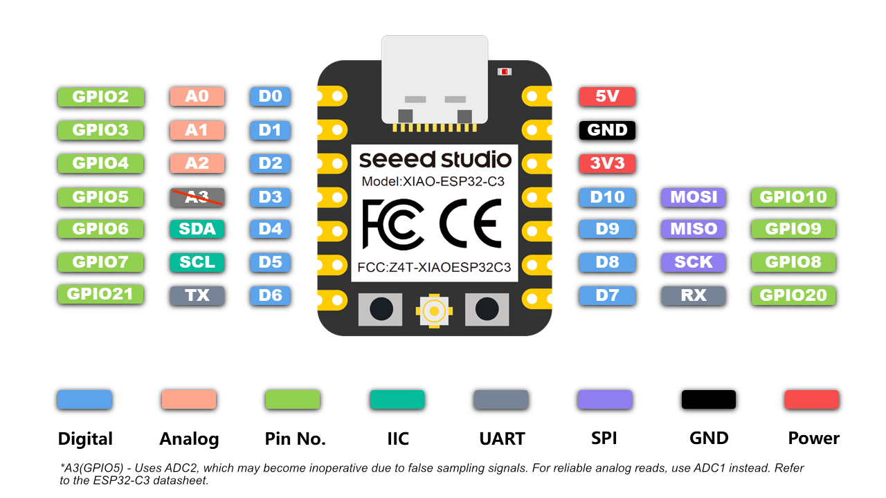
Controller Pinout
I reviewed the XIAO ESP32-C3 pinout before assigning the LED outputs. This was important because the schematic must match the pins that will later be used in the code. I treated the pinout as a bridge between electronic design and embedded programming.
The pinout also helped me understand that the XIAO ESP32-C3 is not only used to turn LEDs on and off. It also provides communication options such as USB serial and available GPIO pins that can be used for external devices in future iterations.
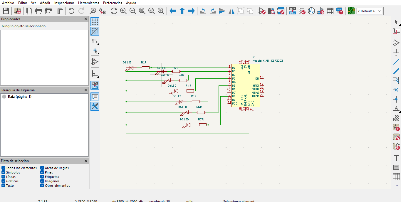
Schematic Design in KiCad
The schematic was the first formal step of the individual board. I placed the XIAO ESP32-C3 symbol, added seven LED and resistor pairs, and connected each LED circuit to an independent GPIO pin. I also checked that each LED had its own resistor, because this is necessary to protect the output pins.
In this step I focused on electrical logic, not on the final physical shape. The schematic helped me answer what each component does, where each signal goes, and how the circuit should behave.
Schematic Checks
| Check | Why It Was Important |
|---|---|
| Each LED has one resistor | Prevents excessive current through the LED and microcontroller pin. |
| GPIO pins are assigned intentionally | Makes the future program easier to write and debug. |
| Power and ground references are clear | Reduces mistakes when moving from schematic to PCB layout. |
| Local interaction with the microcontroller | The LED outputs allow the board to show visible responses controlled by the XIAO ESP32-C3. |
| Microcontroller communication remains accessible | The XIAO USB connector and header pins allow programming, serial communication, and future expansion. |
| ERC review | Allows KiCad to detect missing connections or schematic warnings before moving to PCB layout. |
Pin Assignment
I assigned the LED outputs in a way that makes the sequence easy to understand. Each signal corresponds to one LED and one resistor pair. This organization also helps when writing the LED sequence in code, because the pins can be placed in an ordered array.
| Signal | Function | Connected Element |
|---|---|---|
| GPIO output 1 | Digital output | LED 1 through 220 ohm resistor. |
| GPIO output 2 | Digital output | LED 2 through 220 ohm resistor. |
| GPIO output 3 | Digital output | LED 3 through 220 ohm resistor. |
| GPIO output 4 | Digital output | LED 4 through 220 ohm resistor. |
| GPIO output 5 | Digital output | LED 5 through 220 ohm resistor. |
| GPIO output 6 | Digital output | LED 6 through 220 ohm resistor. |
| GPIO output 7 | Digital output | LED 7 through 220 ohm resistor. |
| USB | Programming and serial communication | Connection between the XIAO ESP32-C3 and the computer. |
| Available XIAO pins | Expansion and external communication | Possible connection for future sensors, outputs, or communication modules. |
| GND | Reference | Common ground for the LED circuit. |
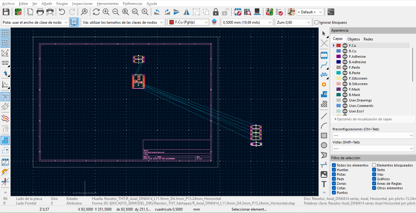
Footprints and Component Placement
After completing the schematic, I assigned footprints and moved to the PCB editor. This step transformed the electrical circuit into a physical board design. I placed the XIAO footprint first because it defines the main scale and orientation of the board. Then I organized the LEDs and resistors around the controller.
I used the ratsnest lines as a guide for placement. When the components are placed carefully, the routing becomes cleaner and the design is easier to read.
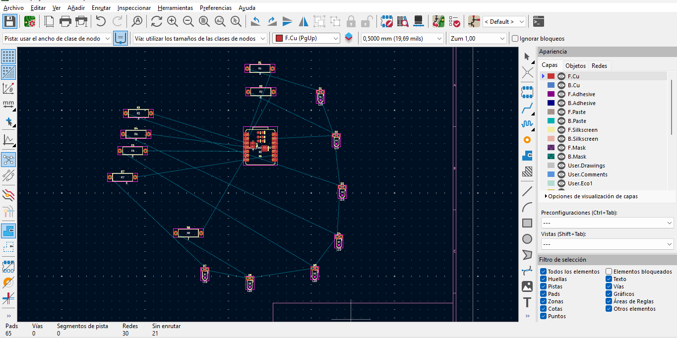
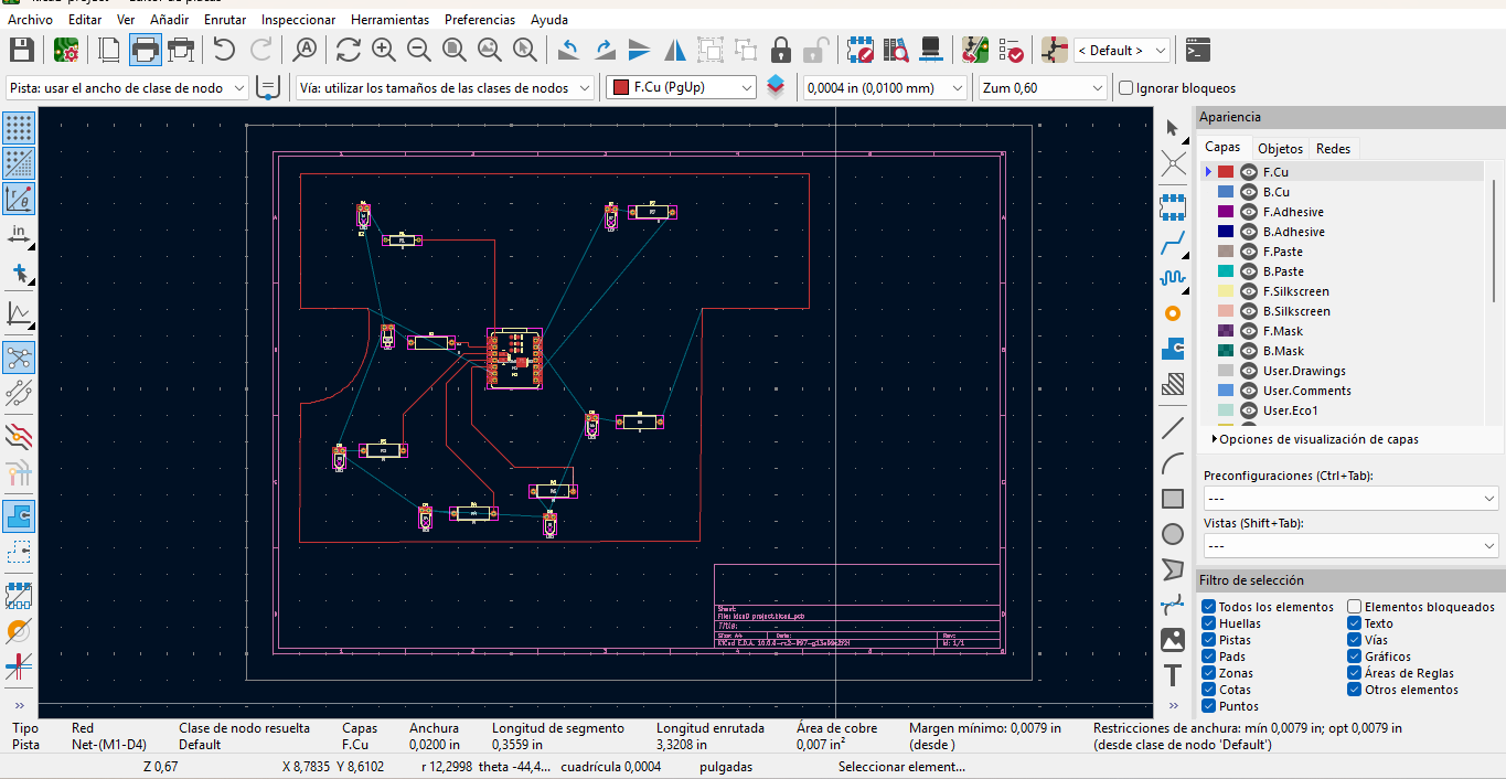
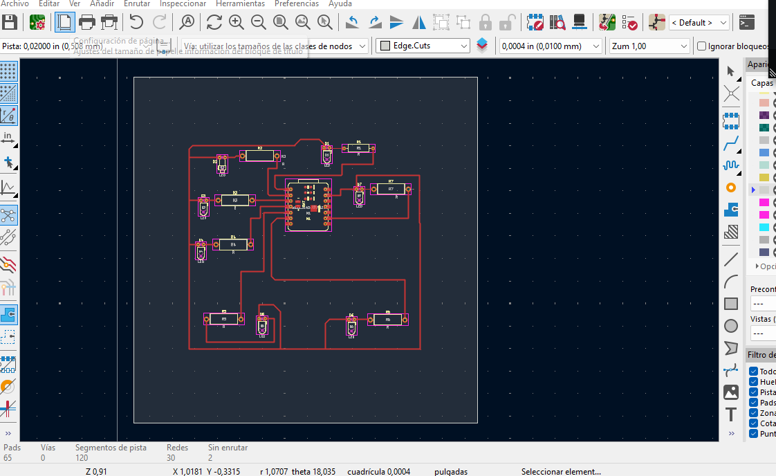
Routing Process
In the routing stage I connected the pads using PCB traces. I routed each LED output from the XIAO ESP32-C3 to the corresponding resistor and LED. I kept the layout readable so the board could be reviewed visually and checked with KiCad design rules.
The most difficult part was routing the traces around the XIAO ESP32-C3 without crossing other nets. The first placement created several long ratsnest lines and some LED/resistor groups were too far from their pins. I solved this by moving components around the controller, routing the shortest signals first, and leaving the longer return paths for the final stage.
Design Rules, ERC and DRC
I established the design rules before finishing the board routing. My criteria were based on three needs: the traces had to be easy to read, the pads had to be accessible for the components, and the board had to pass KiCad checks without leaving unconnected nets. I used the KiCad PCB editor to work with a 0.5000 mm track width during the main routing process.
The rule setup was not only a software step. It was a design decision: thicker traces were easier to review, resistor and LED pads needed clear space around them, and the XIAO ESP32-C3 footprint required enough room for its two rows of pins. I checked the schematic with ERC and then reviewed the routed board with DRC.
To check that the board could be fabricated, I reviewed the trace width, pad spacing, component clearance, board outline, and unrouted nets in KiCad. I used DRC and visual inspection as the main verification steps before exporting the final design files.
To document the fabrication check more clearly, I opened the KiCad board setup window and reviewed the Design Rules section. In the Spanish interface, this panel appears as Reglas de diseño. This panel allowed me to verify the requirements and constraints used for the PCB, including track width, clearance, via settings, and routing rules before exporting the final design files.
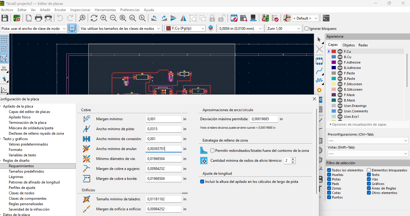
| Rule / Check | Value or Criterion | Reason |
|---|---|---|
| Track width | 0.5000 mm / 19.69 mil during the main routing process | I used a visible and robust trace width for the LED output routes. |
| Clearance between traces | Kept visually separated during routing | I avoided crowded traces near the XIAO pins and LED/resistor pads. |
| Pad accessibility | Clear space around LEDs, resistors, and XIAO pads | The design had to be easy to inspect and understand after layout. |
| Board outline | Reviewed before exporting | The board edge had to contain the routed circuit and allow the XIAO USB connector to remain accessible. |
| Design Rules panel | Reviewed in KiCad Board Setup / Reglas de diseño | I checked the formal board constraints such as track width, clearance, via settings, and routing requirements. |
| Fabrication check | Reviewed with DRC and visual inspection | I checked that traces, pads, and spacing could be fabricated and inspected clearly. |
| ERC | Reviewed after schematic connection | I checked for missing electrical connections before moving to PCB layout. |
| DRC | Reviewed after routing | I checked unresolved nets, trace spacing, and board outline consistency. |
ERC and DRC Results
During the schematic stage, the main ERC issue was related to connections that were visually close but not electrically connected. I corrected this by reconnecting the LED and resistor nets directly to the XIAO pins and checking that every LED had its resistor in series. In the PCB stage, the DRC showed unrouted nets while the board was still in progress. I solved this by following the ratsnest lines until the missing connections were reduced and the final traces matched the schematic.
The checks helped me understand that ERC and DRC are not final buttons to press at the end; they are tools that guide the design process while the board is still changing.
| Check | Problem Reported | Cause | Correction |
|---|---|---|---|
| ERC | Unconnected or incomplete schematic nets. | Some wires looked aligned but were not snapped to the symbol pins. | I reconnected the LED/resistor nets directly to the XIAO pins and reviewed each output line. |
| ERC | Outputs needed clear current-limiting components. | The LED circuit had to be checked so each output included its series resistor. | I verified the seven LED-resistor pairs before moving to PCB layout. |
| DRC | Unrouted nets during early layout iterations. | The first component placement created crossed ratsnest lines and incomplete traces. | I moved the footprints and routed each net until the missing connections were resolved. |
| DRC | Trace spacing needed visual review near the XIAO pins. | Several traces converged around the two pin rows of the controller. | I adjusted the path of the traces and kept the routing width consistent. |
| Fabrication review | The design needed to be checked before exporting. | A PCB can look complete but still contain spacing, outline, or unrouted net issues. | I reviewed trace width, clearance, pad access, board outline, and the Design Rules panel before preparing the final files. |
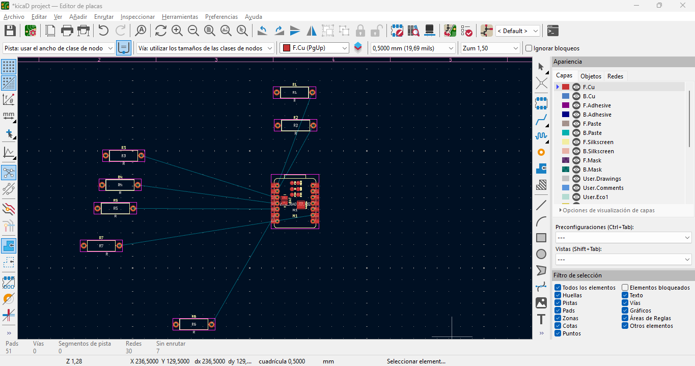
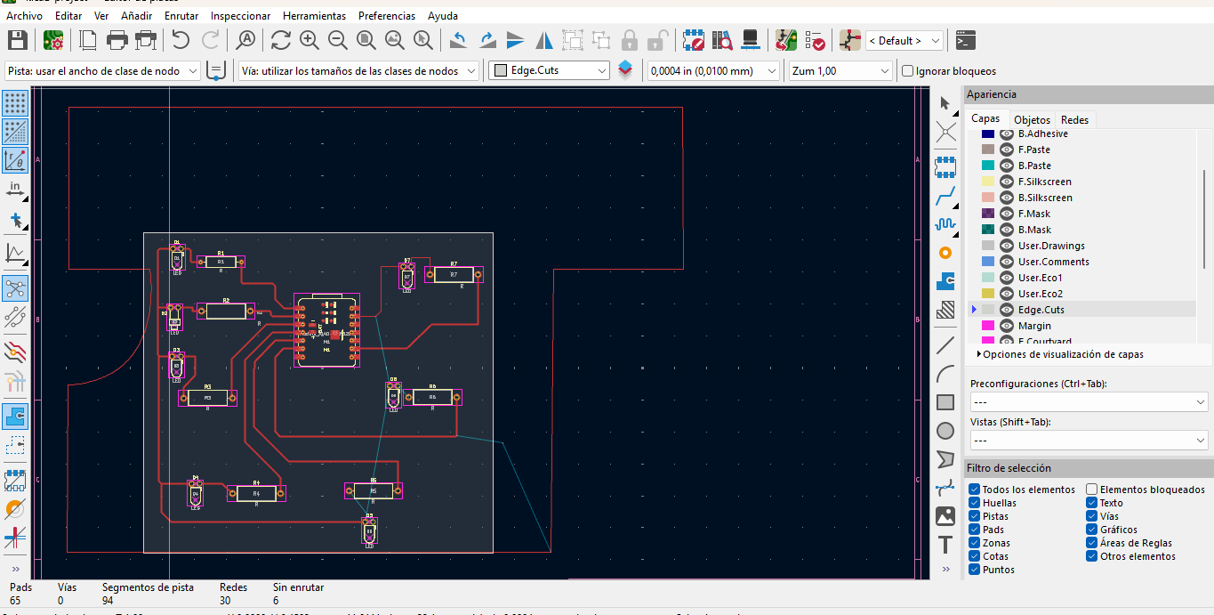
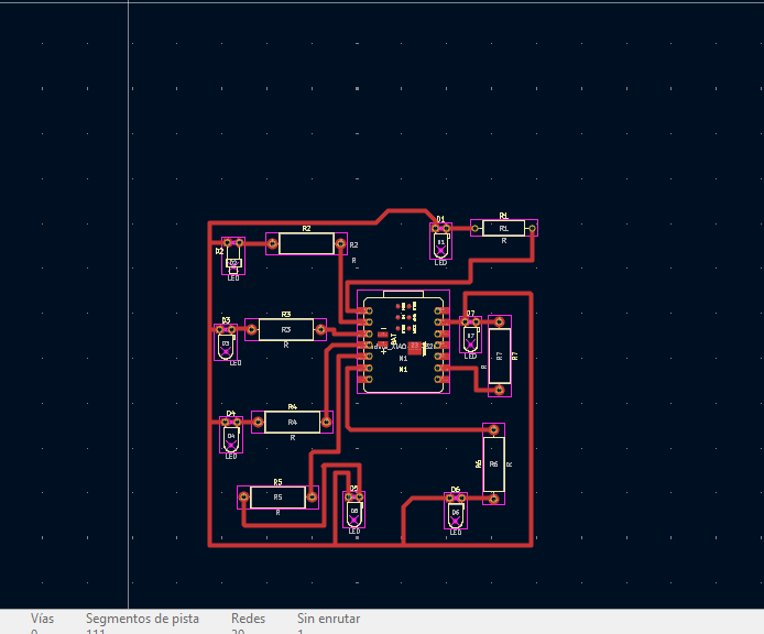
PCB Layout and Routing
The final PCB layout shows the complete physical organization of the LED roulette board. The XIAO ESP32-C3 is located near the center of the board, while the LEDs and resistors are distributed around it to create the roulette effect. The copper traces connect each GPIO output to its resistor and LED path.
The most important design decisions were component spacing, trace organization, pad accessibility, fabrication readability, and board outline. These decisions are part of good electronics design because they make the board easier to inspect, review, fabricate, and improve.
| Design Rule / Criterion | How I Applied It |
|---|---|
| Trace readability | Routes were kept clear and separated where possible. |
| Pad accessibility | Pads were kept visible and not crowded by neighboring components. |
| Component spacing | LEDs and resistors were moved several times to reduce crossed ratsnest lines. |
| Communication access | The XIAO USB connector and header areas were kept accessible for programming and external communication. |
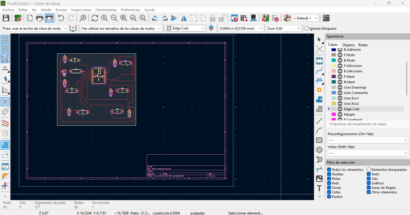
| Board outline | The board edge was defined in the PCB editor. |
| Design rule check | The routed layout was reviewed before exporting the final design files. |
Fabrication Readiness Check
Before considering the design complete, I checked that the PCB could be fabricated. For this step, I inspected the board in KiCad using DRC and visual review. I checked that the traces were continuous, that there were no critical unrouted nets, that the pads were accessible, and that the board outline enclosed the complete circuit without interfering with the USB connector of the XIAO ESP32-C3.
This fabrication check helped me connect the EDA design process with the physical production requirements of a PCB. Even though this assignment focuses on electronics design, the board must still be designed with fabrication in mind.
| Fabrication Aspect | Verification |
|---|---|
| Trace width | The routed traces were made thick enough to be visible, robust, and easy to inspect. |
| Design Rules panel | I documented the KiCad Board Setup panel under Reglas de diseño to show the rule configuration used for the board. |
| Unrouted nets | I followed the ratsnest and DRC feedback to complete the missing connections during routing. |
| Pad spacing | I kept enough space around LED, resistor, and XIAO pads for inspection and soldering. |
| Board outline | The board edge was checked so the full circuit remained inside the final shape. |
| USB access | The XIAO ESP32-C3 USB connector was kept accessible for programming and communication. |
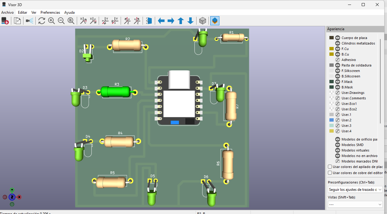
3D View and Final Inspection
After routing the PCB, I used the KiCad 3D Viewer to inspect the board as an assembled object. This step was important because the 2D layout shows the electrical connections, but the 3D view helps verify the physical relationship between components: LED orientation, resistor position, XIAO ESP32-C3 placement, available space between parts, and the general readability of the board.
In the 3D inspection I checked that the LEDs and resistors were not colliding with each other, that the XIAO module was centered and accessible, and that the board shape worked with the component distribution. This final visual check helped me confirm that the PCB design was coherent before exporting the final artwork and downloadable files.
Design Output Files
After the board was routed, I generated design outputs from KiCad and prepared a high-contrast artwork in Inkscape. These files document the result of the electronics design process and allow the board to be reviewed, modified, fabricated, or reused later.
Design Problems and Solutions
| Problem | Design Response | Learning |
|---|---|---|
| Some schematic connections were visually close but not electrically connected. | I corrected the nets in KiCad and checked that each LED-resistor pair connected to the intended XIAO pin. | ERC must be used while drawing the schematic, not only at the end. |
| The first footprint placement created many crossed ratsnest lines. | I moved the resistors and LEDs around the XIAO before routing the final traces. | Good placement is the first routing strategy. |
| Several traces had to pass close to the XIAO pin rows. | I used a robust trace width and kept enough spacing between neighboring tracks. | Design rules help keep the board readable and consistent. |
| Some nets remained unrouted during the first PCB iterations. | I followed the DRC/unrouted net feedback and completed the missing connections one by one. | DRC is useful for finding routing tasks that are easy to miss visually. |
| The board outline had to fit around the routed circuit. | I adjusted the board edge after the main traces were already organized. | The board contour should respond to the circuit, not force the circuit into a difficult route. |
| The board needed to satisfy the development board requirement. | I documented the LED outputs as local interaction and the XIAO USB/header access as communication and expansion options. | A development board must show both microcontroller interaction and a way to communicate or connect with external devices. |
| The evaluator requested evidence of the KiCad Design Rules panel. | I added a screenshot of the KiCad Board Setup window under Reglas de diseño. | Documenting the formal design rules makes the fabrication check clearer and more complete. |
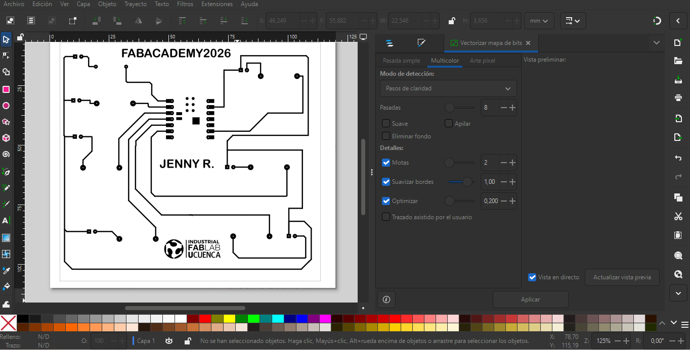
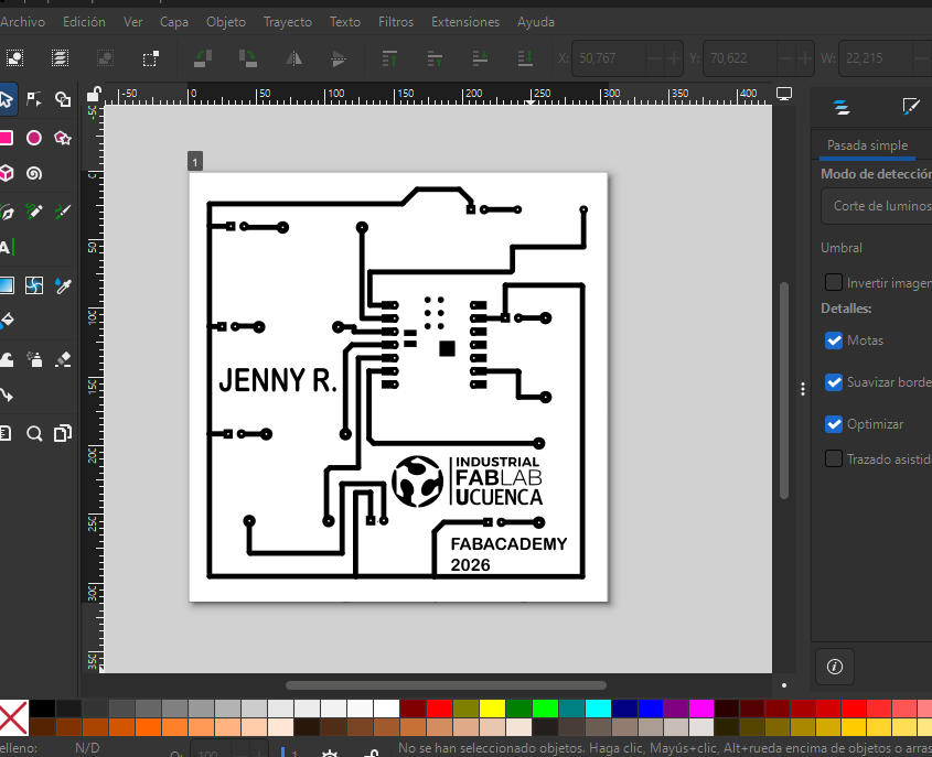
PCB Hero Shot
This is the final PCB artwork generated from the KiCad design. The image shows the board as a high-contrast black-and-white output, with the traces, pads, XIAO ESP32-C3 footprint, LED/resistor connection points, my name, the Industrial FabLab UCuenca logo, and the Fab Academy 2026 label. I used this hero shot to present the final result of the electronics design process in a direct and readable way.
The thick black paths represent the copper traces and connection areas. The circular pads mark the soldering points for through-hole components, while the central footprint corresponds to the XIAO ESP32-C3 module. This final artwork makes it possible to understand the board layout without opening KiCad.
What I Learned
This assignment helped me understand electronics design as a complete chain of decisions. I learned that the schematic defines the electrical intention, while the PCB layout defines how that intention becomes a physical board. If the schematic, footprints, placement, routing, and design rules do not agree with each other, the board will be difficult to understand or modify.
I also learned that a simple board is useful for practicing the full workflow. The LED roulette PCB allowed me to focus on component selection, pin assignment, routing discipline, fabrication checks, and the importance of checking the design before considering any later process.
Another important lesson was that a development board must not only contain a microcontroller, but also provide a way to interact with it and communicate with other devices. In my design, the seven LEDs create local interaction, while the XIAO ESP32-C3 USB connector and available pins allow programming, serial communication, and future expansion.
Finally, I learned that documenting the KiCad Design Rules panel is important because it shows the formal constraints used for the PCB, not only the visual routing result.
Download Design Files
The following files correspond to the original electronic design of the board. These files were created in KiCad and include the project file, the PCB layout file, and the final exported board artwork. They allow the design to be reviewed, modified, fabricated, or reused later.