Week 6: Electronics Design
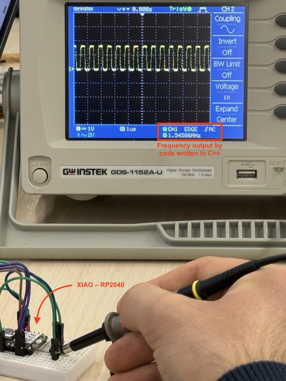 *The logged frequency on the oscilloscope.
Group Assignment
This week’s group assignment objective was to use the test equipment at our lab to observe microcontrollers’ operation. We worked with the GW Instek GDS-1152A-U oscilloscope to learn how to observe these signals, and understood the simplest diffrences of why an oscilloscope can matter more than a multimeter [it shows voltage changing over time in real time]. We wrote a simple counter program, uploaded it onto a RP2040, and wired it to the oscilloscope to watch the operation directly.
It was interesting to see the visualization – the I2C communication between the RP2040 and the LCD, where we could clearly see the yellow SDA data line and the blue SCL clock line working together, with the clock telling the device when to read each bit. We also ran a toggle test to measure how fast the chip could flip a pin: Mariam’s MicroPython interpreter overhead limited the speed, while my C++ version reached about 1.55 MHz showing the evident difference between interpreted and compiled code.
I also will never be able to view bits the same way. The fact that you can freeze a certain signal frame, and visually analyze the 0s and 1s of a bit packet is a complete rediscovery for me. I mean I know what a bit [or a byte for that matter] is… but, before this instance I did not have that image of code in my head. It seems more tangible, and demystifying now!
Schematic Diagrams
During embedded programming week I had watched some videos on YouTube, but this one stood out the most. At the time I though that I would need to know some of the basics of schematics diagrams, but it turned out I needed them a bit later. Apart from this video I had also asked Claude to generate me several grouped cheatsheets for the symbols, the prompt for which you can find at the very bottom.
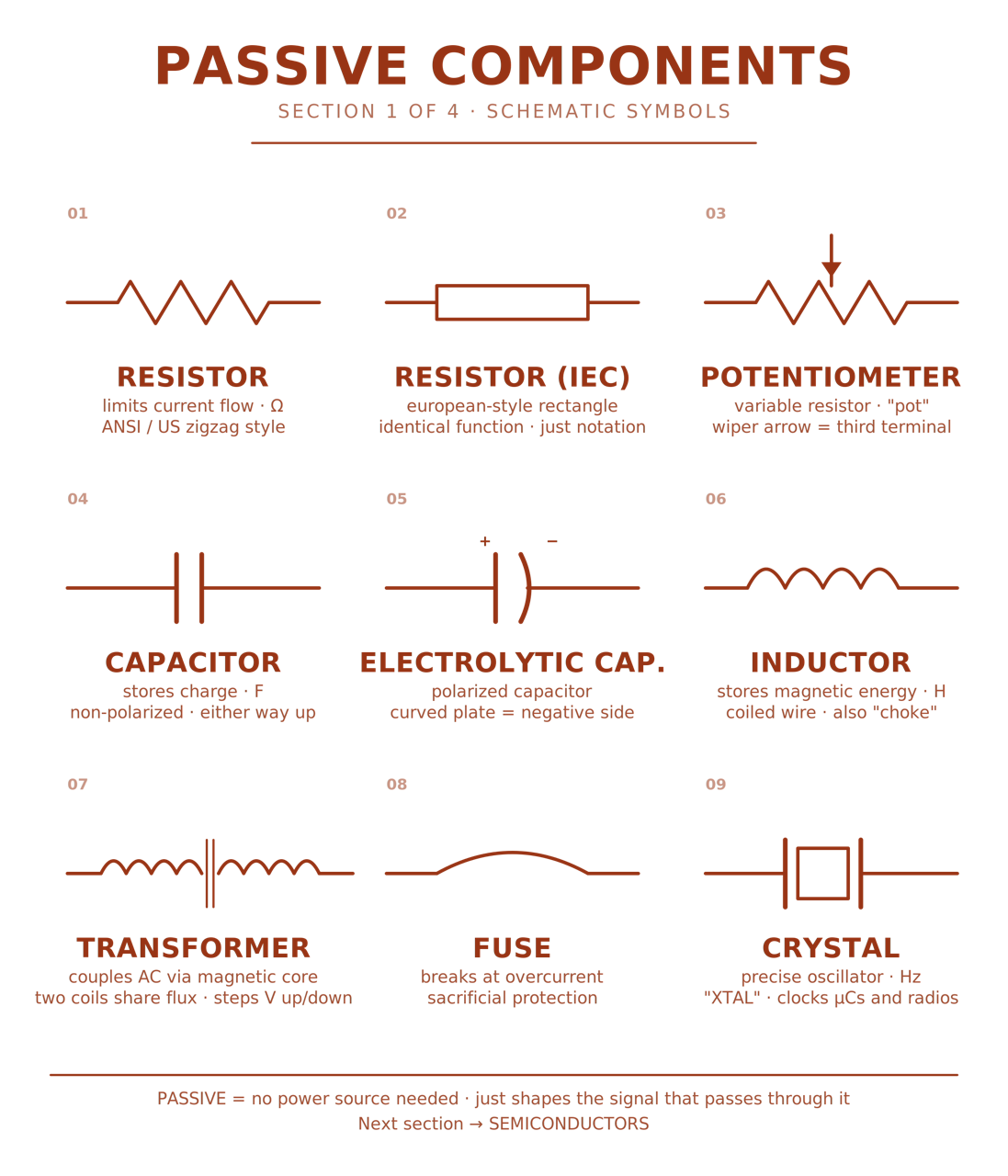
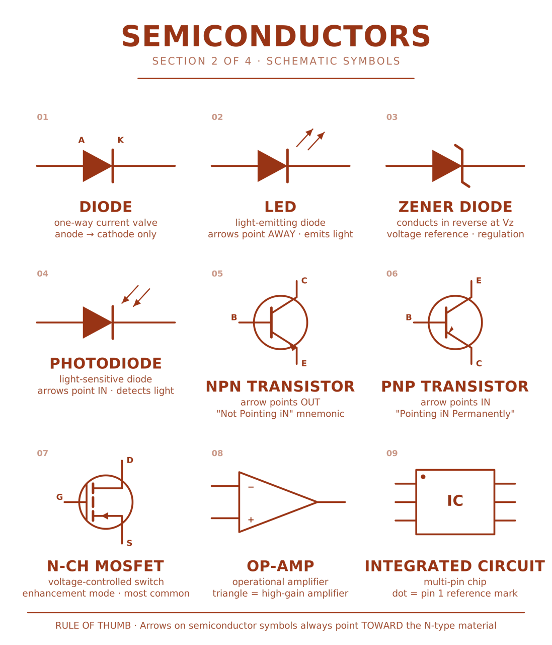
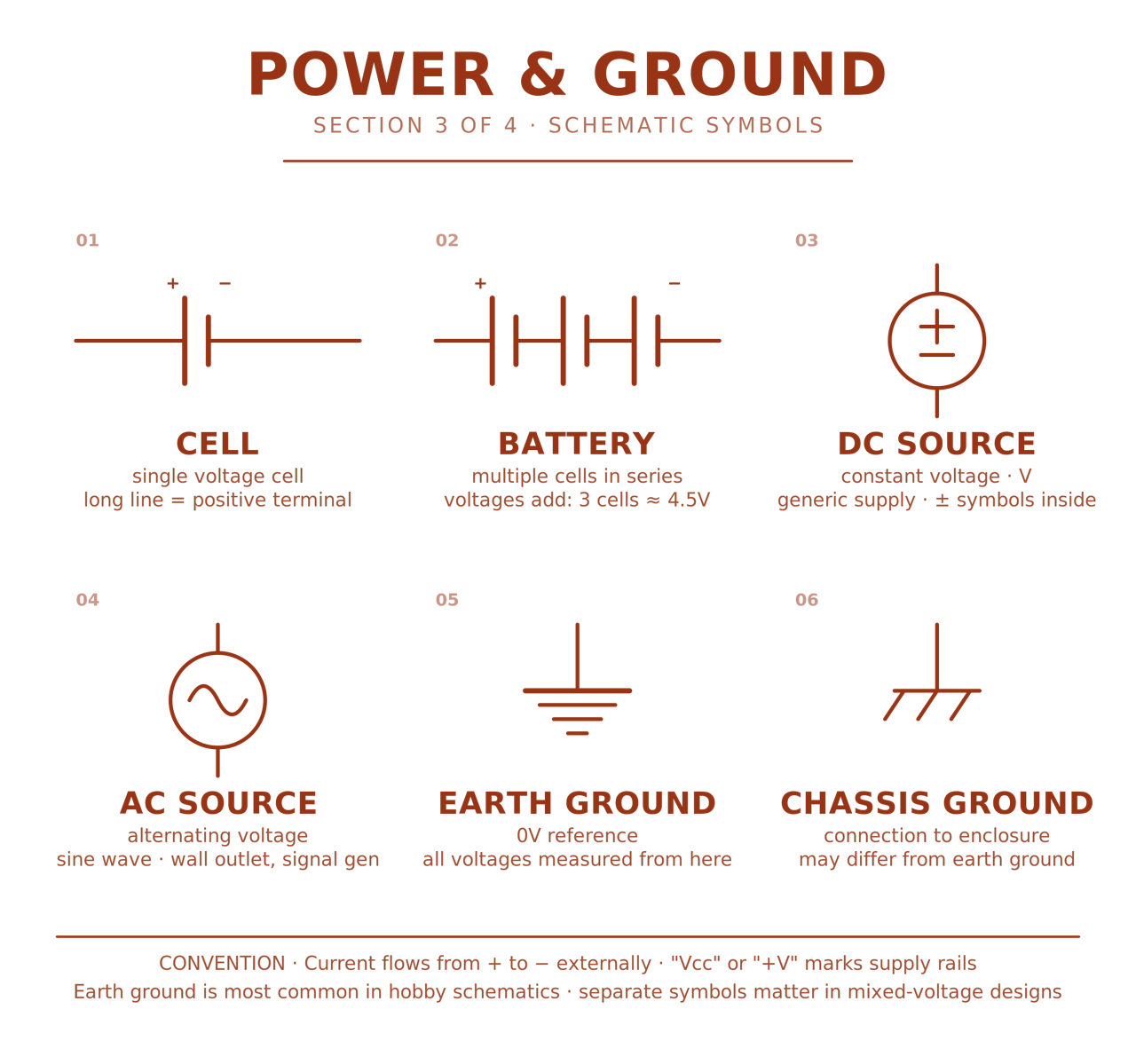
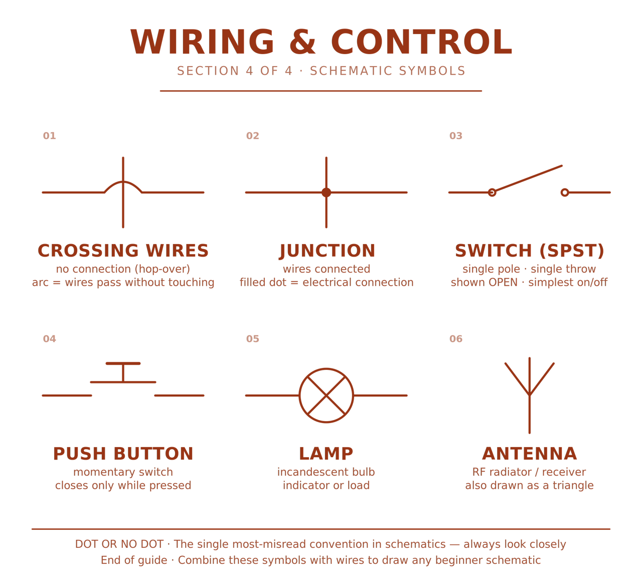
*Prompt6.1
You can download the PDF version down in the Resources section.
What is an Oscilloscope?
Out of all the most common measuring tools we first got acquainted with an oscilloscope. To experiemnt with the output of the testing instrument we’ve taken an XIAO-RP2040 microcontroller board, and wired it on a breadboard. My first interaction with the instrument seemed very complex, but in fact it’s a very simple tool just measuring voltage against time.
Some basic vocabulary: • Voltage: signal strength • Time: signal change duration • Frequency: cycles per second • Period: one full cycle time • Clock: regular timing square wave • Channel: input measurement line • Trigger: stabilizes repeating waveform • Amplitude: signal height from zero
To have a more interesting testing, my groupmate Mariam and I had devided the task into two programming languages and IDEs. By putting the measuring probe onto one of the pins on the MCU, and the grounding clip on to the GND pin, we obtained the toggle frequency of the MCU. Mariam had analyzed the MCU’s performance with MicroPython and Thonny, whereas I converted the same code into C++, combiling through Arduino IDE.
With substantial results: • MicroPython at 694kHz • C++ at 1,55MHz
The Code
C++

#include <Wire.h>

#define SCOPE_PIN 26

int state = 1;

void setup() {
  pinMode(SCOPE_PIN, OUTPUT);
}

void loop() {
  state = 1 - state;
  digitalWriteFast(SCOPE_PIN,state); // toggle pin
}
Individual Assignment
The Library
As we’ve been using XIAO RP2040, which is not included in the default library of KiCad, so I proceeded to download the KiCad FabLib library from git.
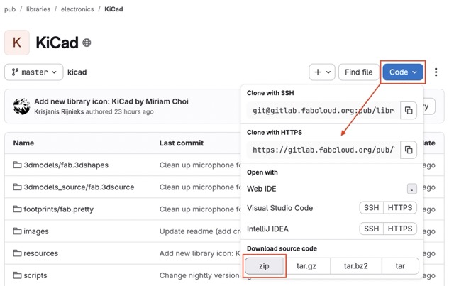
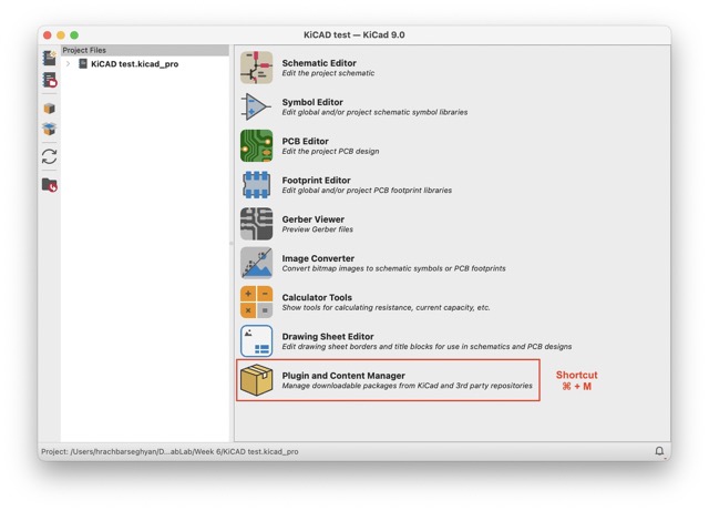
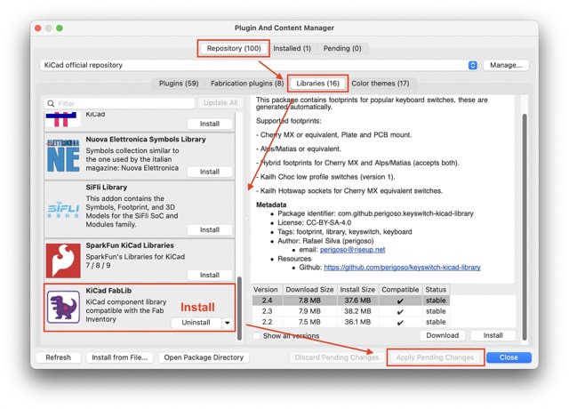
For me, the easiest way to download was following Krisjanis Rijnieks’ steps, from KiCad’s Plugin Repository:
- Tools > Plugin and Content Manager
- Select the Libraries tab
- Look for “KiCad FabLib”
- Click “Install”
- Click “Apply Pending Changes”
LTSpice
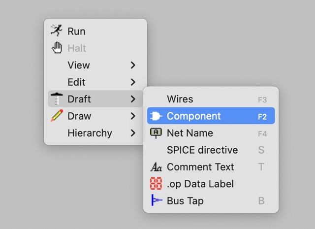
WARNING: LTSpice on Macs!
The app does not have a toolbar placed up top.
To access to the tools: Right-Click > Draft > Component. If you need a ground pin, do not search, press g instead.
I found the basic tutorials on their website to be very useful. Although bare with patiece, I couldn’t find tools to speed up the process.
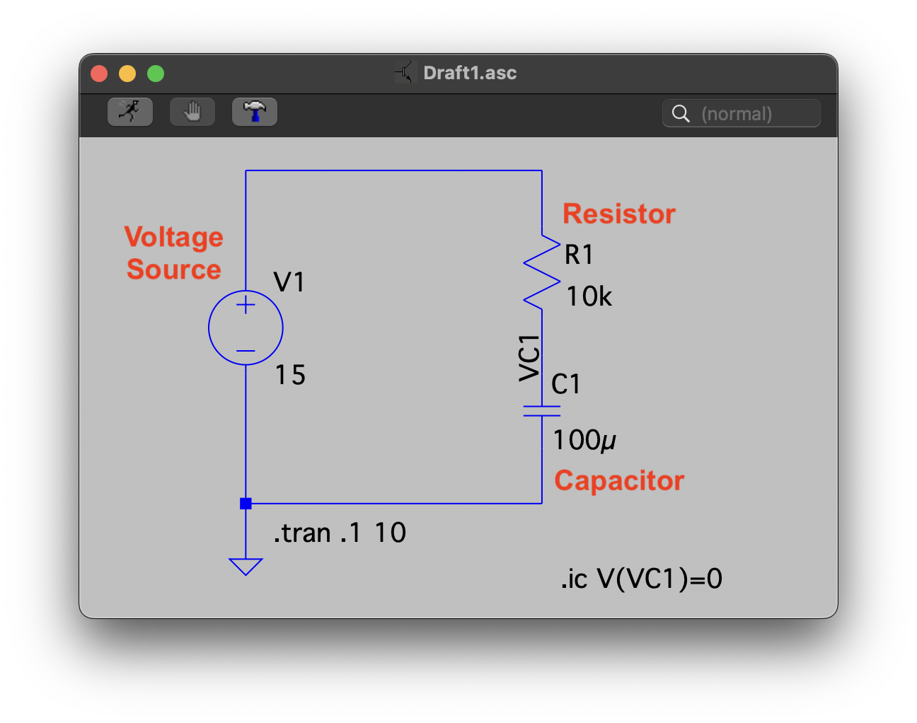
To give value to components: right-click on the bottom letter next to the component. In an example with the power source, by default there is V1 – the number of power source, and V – the measuring unit of the given component [in this case Volts].
To simulate on the schematic:
• on Windows press “.op” in the toolbar
• on Mac right-click > Draft > SPICE directive [or press S]
Note: here’s also where you can make comments, disregarded by the simulator.
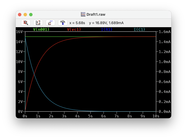
Transient simulation is analysis of voltage spikes obsereving changes within a short segment of time, whereas transient itself means lasting a short period of time.
KiCad
KiCad is a number of interconnected apps, e.g. Schematic Editor, PCB Editor, etc. For now I will focus on these two.
Schematic Editor
Proceeding with Schematic Editor and the individual assignment, I started sketching out a PCB for a drone free-fall detector, and parachture deployment unit documented in week 2.
The components of the board are: 1x XIAO RP2040 1x GY-521 Accelerometer and Gyroscope 1x Buzzer 1x LED 1x Actuator [for the door latch]
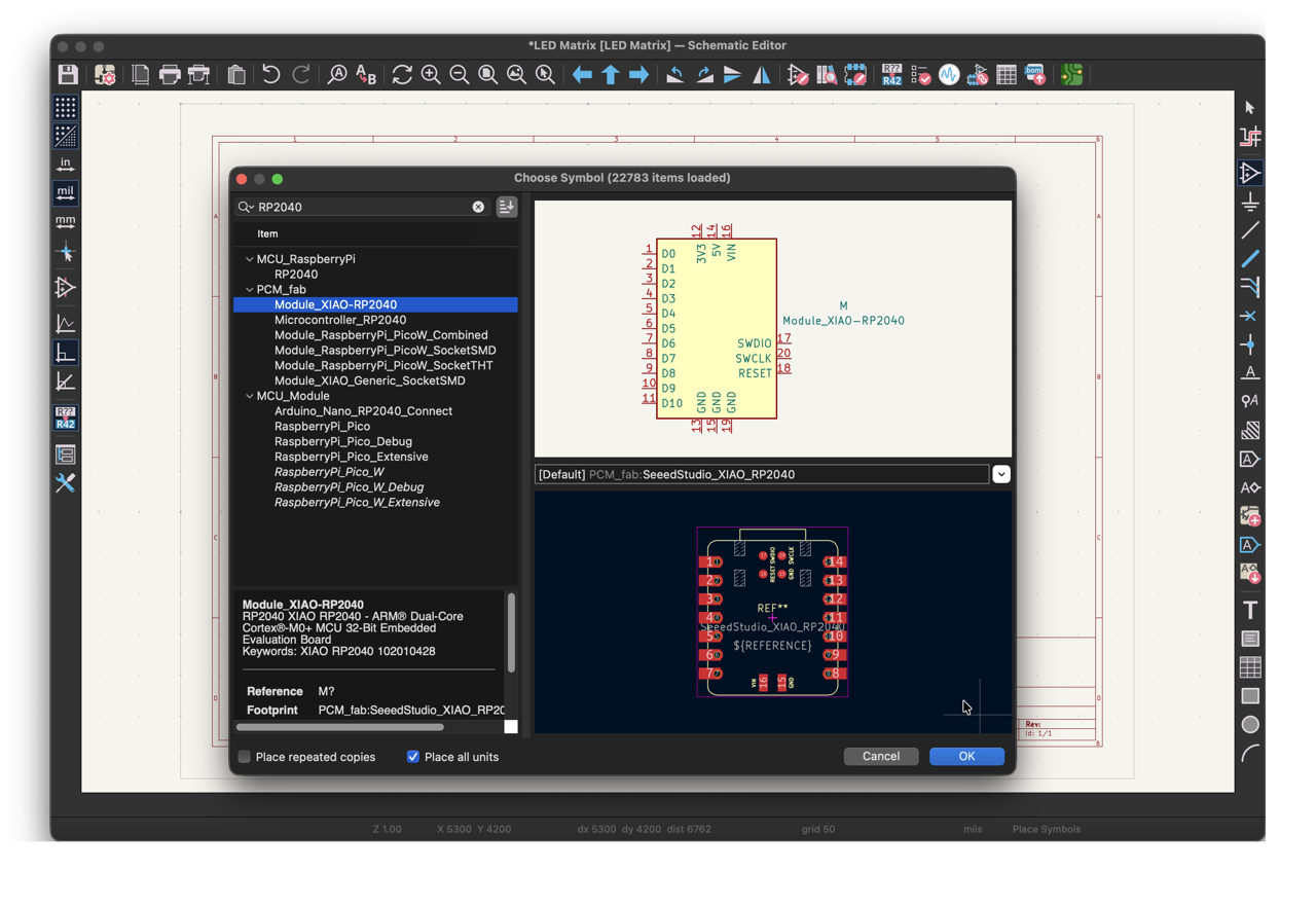
I first started placing components. To add a symbol I pressed the hotkey A, searched for “RP2040,” and drop it onto the sheet. I press A again for each of my other components and place them near the RP2040.
Here’s a basic step-by-step on adding an LED, a resistor and an RP2040:
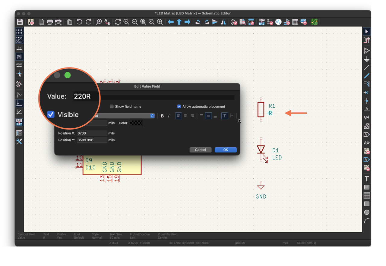
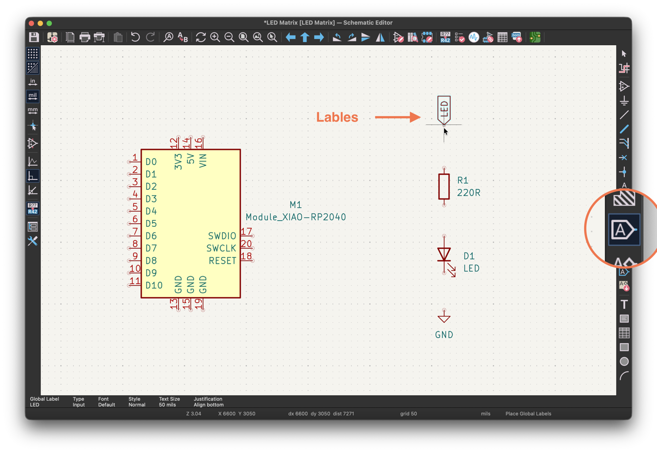
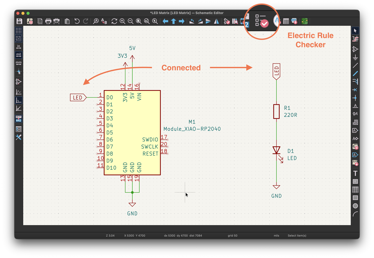
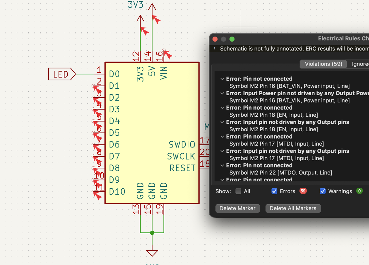
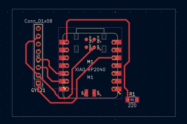
For the GY-521 gyroscope, I didn’t have a 3D model or footprint downloaded, so instead of using a dedicated symbol I simply placed an 8-pin connector to represent it. This way I can still wire it into the design and physically connect the real module later. I also added an LED and changed its series resistor value to 220 Ω to limit the current, plus a 5 V passive buzzer for sound feedback.
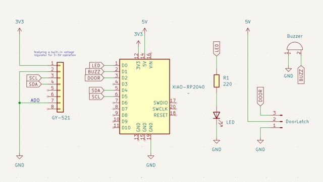
Finally, I included a door latch conceptually – I’m not yet sure how it will work mechanically in the future, but I knew it would need three lines, so I gave it a power line, a GND line, and a data line to plan ahead.
Instead of drawing long wires everywhere, I use labels to keep things clean. I hovered over a pin and press L to add a net label, then typed a name like SDA. I gave the matching pin on another component the exact same label SDA. In KiCad, any pins sharing the same label name are electrically connected, even without a visible wire. For short connections I just pressed W to draw a wire directly [just like between the resistor and the LED], and I add power symbols [press P] for VCC and GND.
PCB Editor
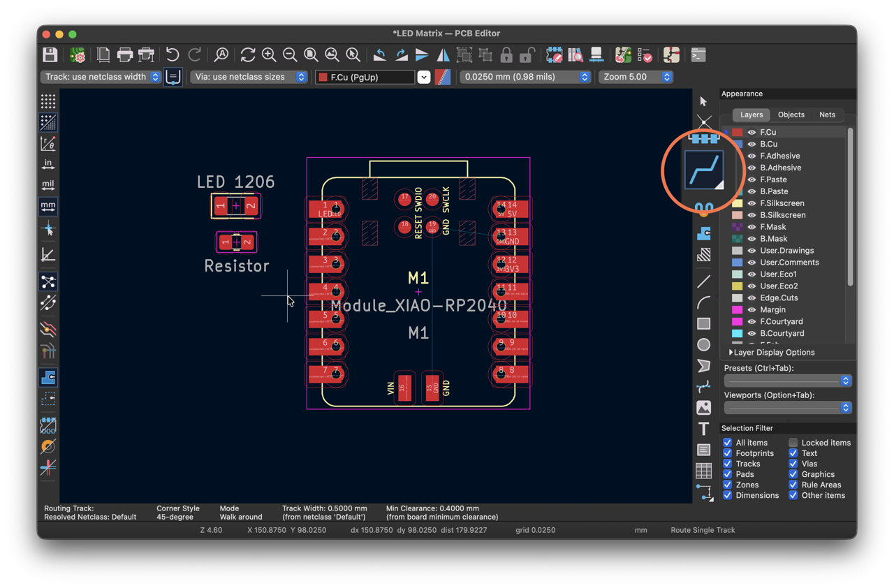
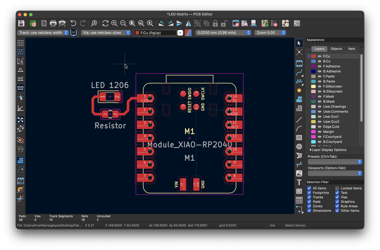
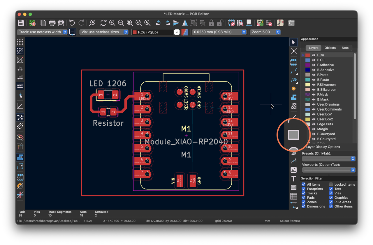
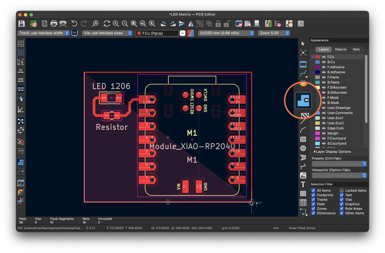
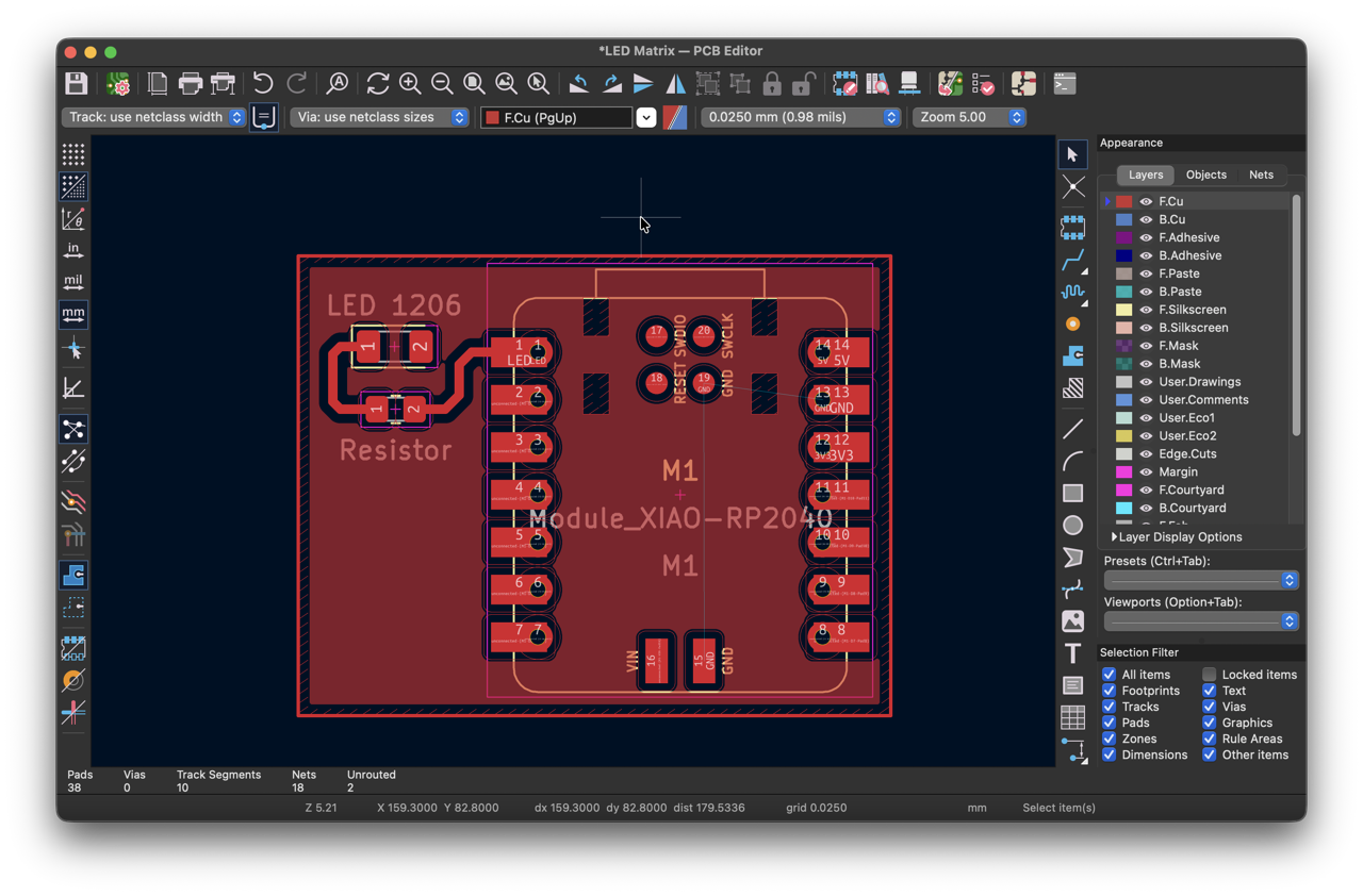
Another quick step-by-step on the PCB design:
DRC Checker
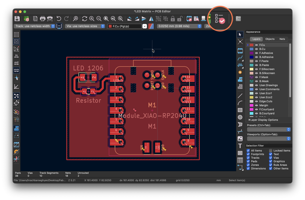
Finally I ran the Design Rule Checker [DRC], which automatically checks my layout against rules like clearances and trace widths to catch shorts or missing connections. I fixed anything it flags until it reports 0 errors, and then the board is ready for milling.
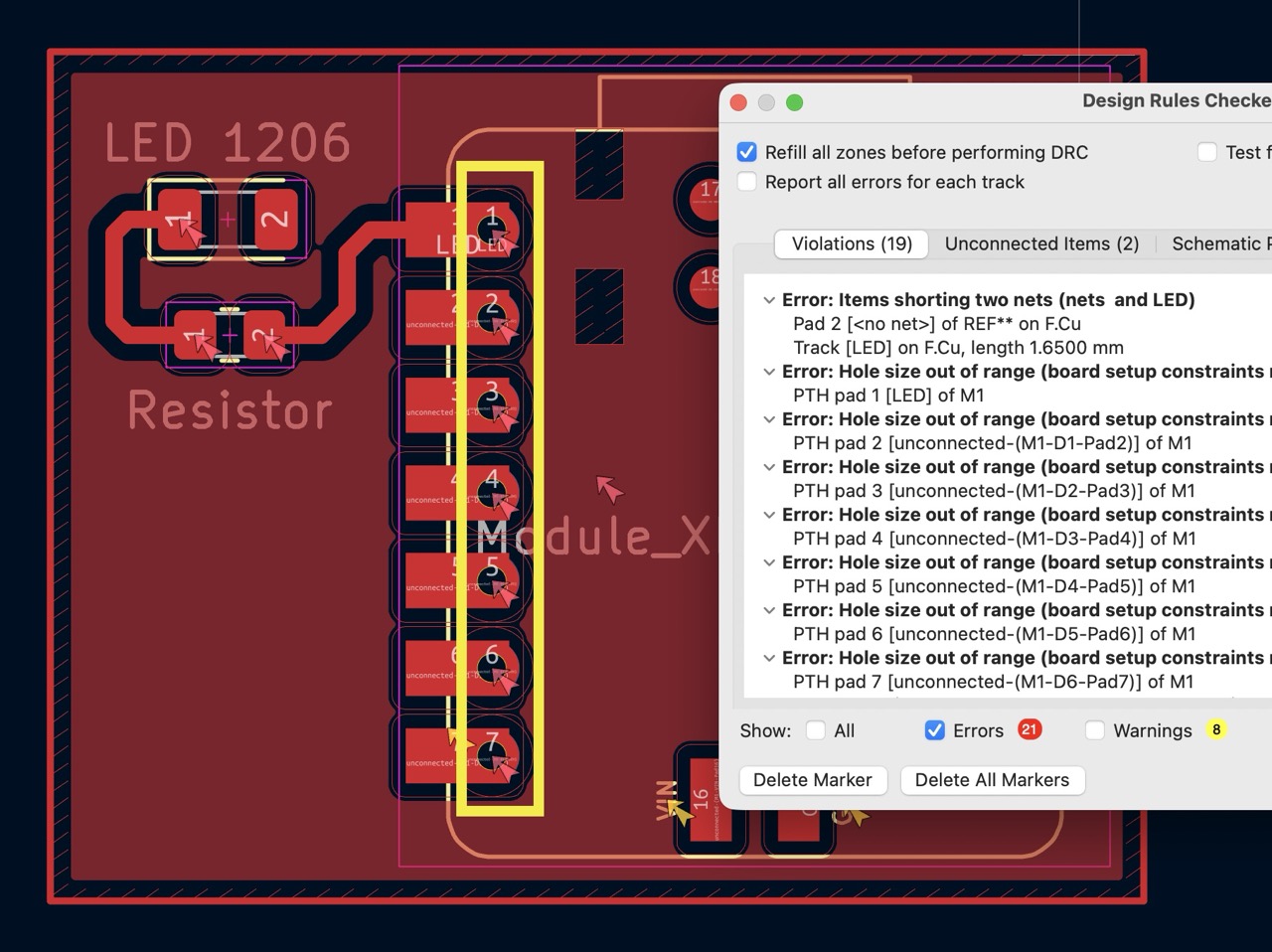
Once every pin had either a wire or a matching label, my schematic was complete. Now I had moved to PCB design, again in Kicad. I clicked Switch to PCB Editor to bring all the components across. They appear with thin “ratsnest” lines showing which pads need to connect, based on my schematic. I dragged the footprints into a sensible layout and route the connections, then use a filled zone for GND to cover the board.
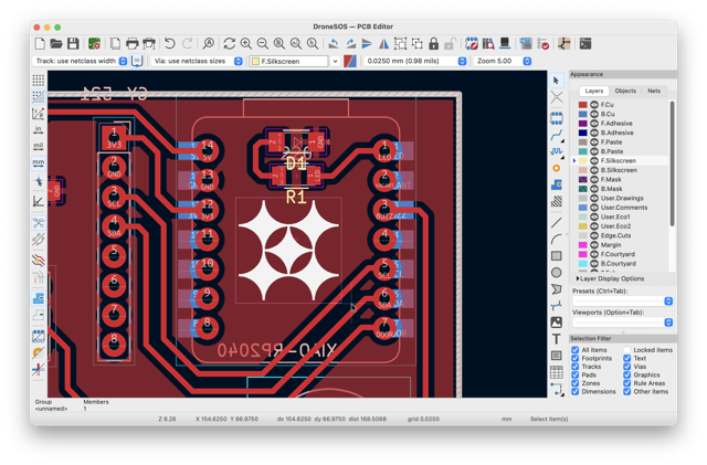
I also wanted to engrave something that would indicate the author of the PCB, and as I did not want to write “Hrach” on it, or perhaps give it a name, I simply placed my favicon.
It’s quite simple, you go to:
Selecting solkscreen ensures the milling bit does not cut through, it simply takes a thin copper layer off. And as I was planning to attach female connectors for the RP2040, and not surface mount the chip, placing the logo on the footprint will not cover the engraving.
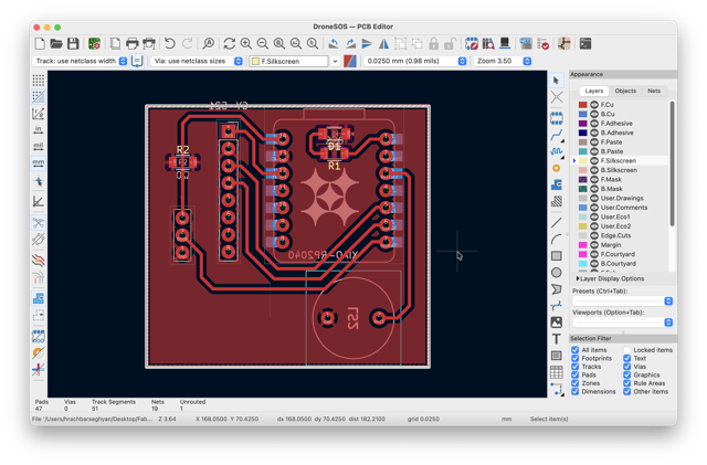
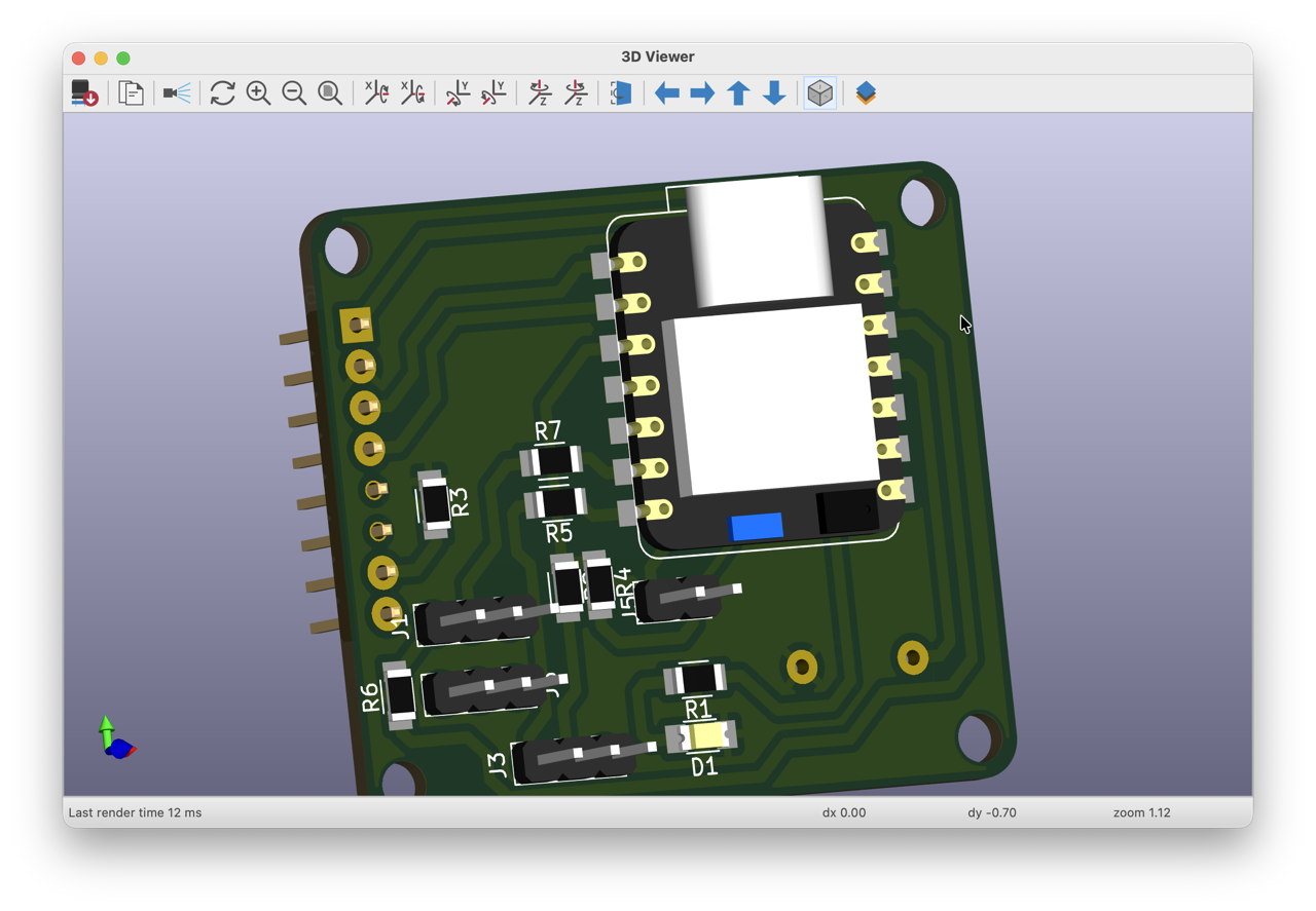
After some back and forth my design ended up looking like this:
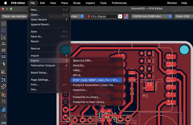
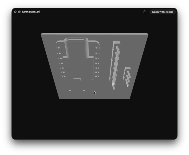
Export as 3D
Conclusion
One big takeaway for me is my paradugn shifting. Learning the types of measuring devices, even at a very basic level of what a certain gadget is responsible for, let me focus on more important aspects of electronics. Before this I had seen some of these devices at my univerity’s labs, but I had no understanding whatsoever to even visually set them apart. The world of electronics seemed very distant because of this barrier, but now I am more open to the knowledge just because these walls had been crushed. Now I also know what tool I should reach for for a given need.
Resources
• Schematics Symbols
• PCB Design
• PCB STL
Prompts
Prompt6.1 Create a beginner’s reference guide for basic electronic schematic symbols as transparent-background PNGs, using rgb(152,52,21) for all outlines and text. Split the content into clear sections: passive components, semiconductors, power and ground, wiring and control. Keep the visual style consistent across all sheets.