Assignment 8: Electronics Production
In this assignment, we learned about electronics production, including PCB milling and operating a PCB milling machine. We practiced soldering techniques to assemble components onto our PCB boards. Understanding the correct placement and orientation of components was crucial for a successful assembly. We also explored troubleshooting methods to check for soldering defects and ensure proper connections. Overall, this assignment helped us gain hands-on experience in fabricating and assembling electronic circuits.
Highlight Moments of the Week
PCB Fabrication
Etching for PCB Fabrication
Etching is a process used to remove unwanted copper from a PCB to create circuit traces. It involves transferring the PCB design onto a copper-clad board and then using a chemical solution like ferric chloride to dissolve the excess copper. Before etching, a protective layer (such as toner or UV-resistant ink) is applied to the desired traces to prevent them from being removed. The board is then submerged in the etching solution, and agitation helps speed up the process. Once the excess copper is removed, the board is cleaned, and holes are drilled for component placement. for More information
Material removal (engraving) for circuit board production
Material removal, also known as engraving, is a method used to create circuit paths on a copper-clad board. A high-speed cutting tool scrapes away unwanted copper, leaving only the required connections. This process is controlled by a programmed machine that follows precise coordinates to ensure accuracy. Unlike chemical etching, engraving does not involve harmful solutions, making it a cleaner alternative. The depth and width of the cuts depend on the tool size and material properties. Proper speed and feed rate settings are crucial to prevent damage to the board. After engraving, the board is cleaned to remove debris before component assembly. This method is widely used for rapid prototyping and custom PCB manufacturing. for More information
Material, Machine and Tools used in PCB Machining (Milling) for my Electronics Production:
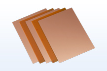
Material:
- FR1-Phenolic paper is a type of insulating material used for making low-cost printed circuit boards. It is made from layers of cellulose paper soaked in phenolic resin, giving it good mechanical strength and electrical insulation. This material is easy to machine and drill, making it suitable for prototyping and simple electronics. Unlike fiberglass-based boards, FR1 is less durable but provides good heat resistance for basic applications. It is commonly used in single-layer PCBs due to its affordability and ease of processing.
References: Reference,
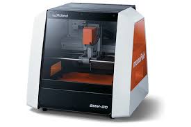
Machine:
The SRM-20 milling machine is a compact and precise desktop CNC used for PCB fabrication and prototyping. It operates by cutting away unwanted copper from a board using small milling bits. This machine follows G-code instructions to carve circuit traces with high accuracy. It supports different tool sizes, allowing for fine detail work and efficient material removal. The SRM-20 is user-friendly, making it suitable for beginners and experienced users alike. It requires careful speed and depth settings to avoid damaging the PCB. Regular maintenance, such as cleaning dust and checking tool alignment, ensures consistent performance. This milling machine is widely used for custom circuit board production and other precision machining tasks.
References: Reference,
Tools:
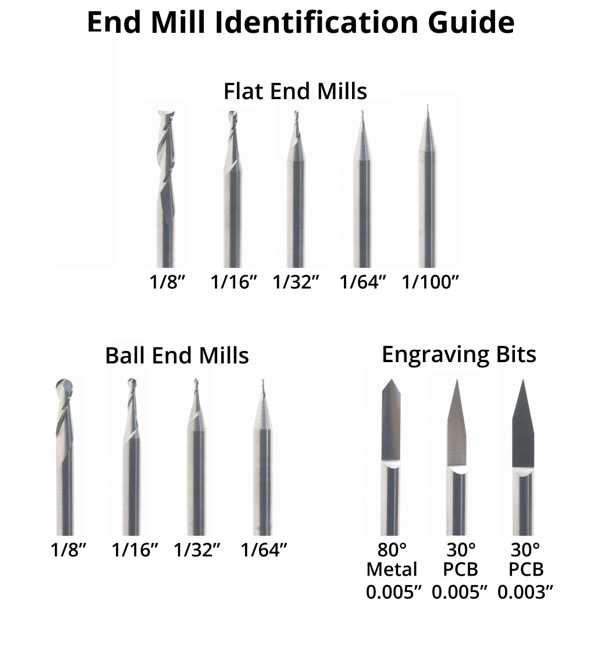
PCBs can be fabricated using conventional end mills. Flat end mills offer several benefits due to their straight profiles and uniform diameters, which help maintain consistent trace widths, even if the FR-1 PCB blank isn’t perfectly level. Additionally, flat end mills excel at removing large sections of material efficiently, with larger ones capable of rapid material removal.
References: Reference,
PCB assembly
PCB assembly is the process of soldering electronic components onto a printed circuit board (PCB) to create a functional electronic device. It involves placing and soldering components such as resistors, capacitors, ICs, and connectors onto the board. Read More,
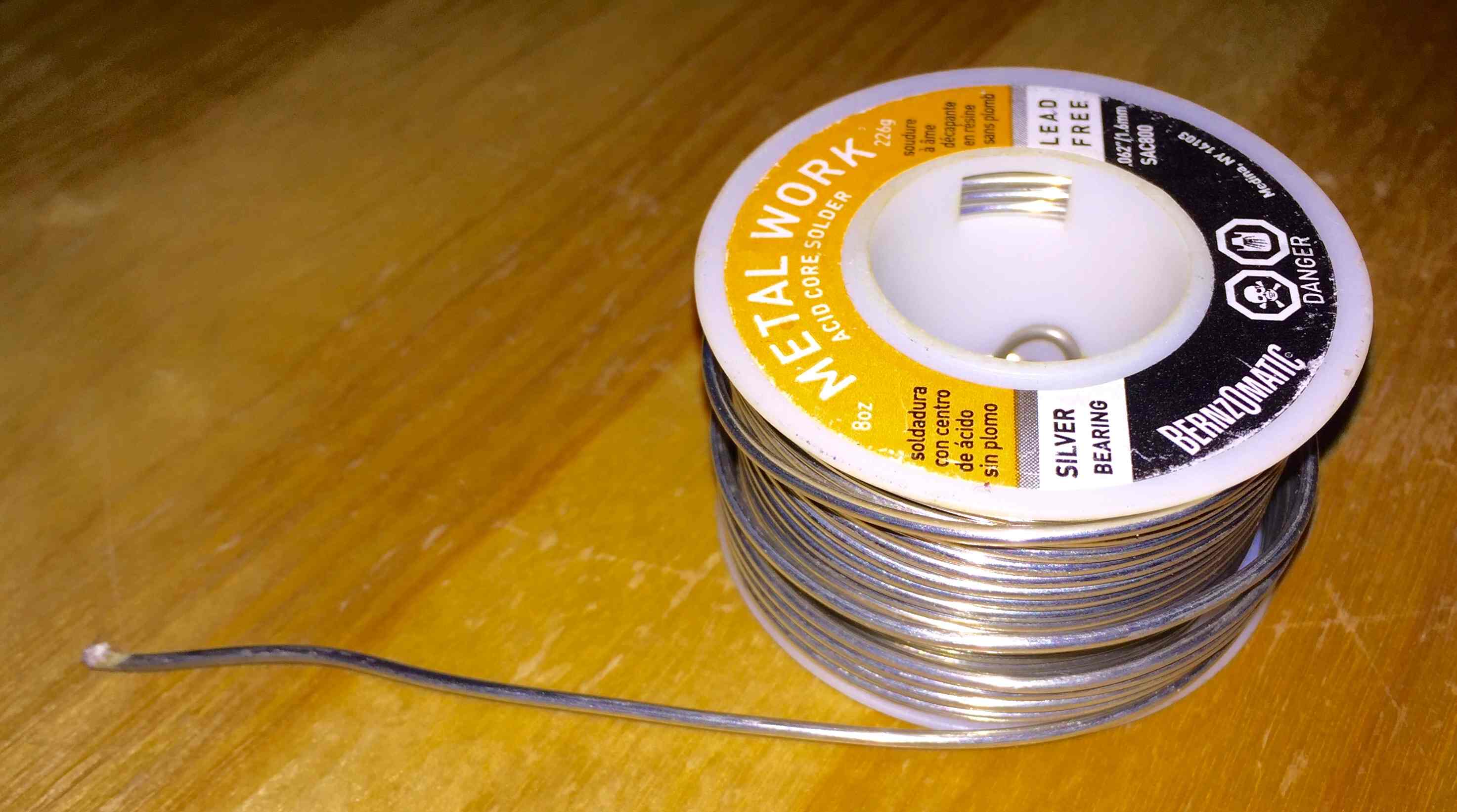
Solder is a metal alloy used to join electronic components to a PCB by melting and bonding them securely. It creates a strong electrical connection between component leads and copper traces on the board. The most common types are lead-based and lead-free solder, each with different melting points and properties.
References: Reference,
Solder paste is a thick mixture of tiny solder particles and flux, used in PCB assembly to connect surface-mount components. It is applied to the board using a stencil before components are placed, and then melted during reflow soldering to form strong electrical connections. This process ensures precise and efficient soldering for modern electronics.
References: Reference,
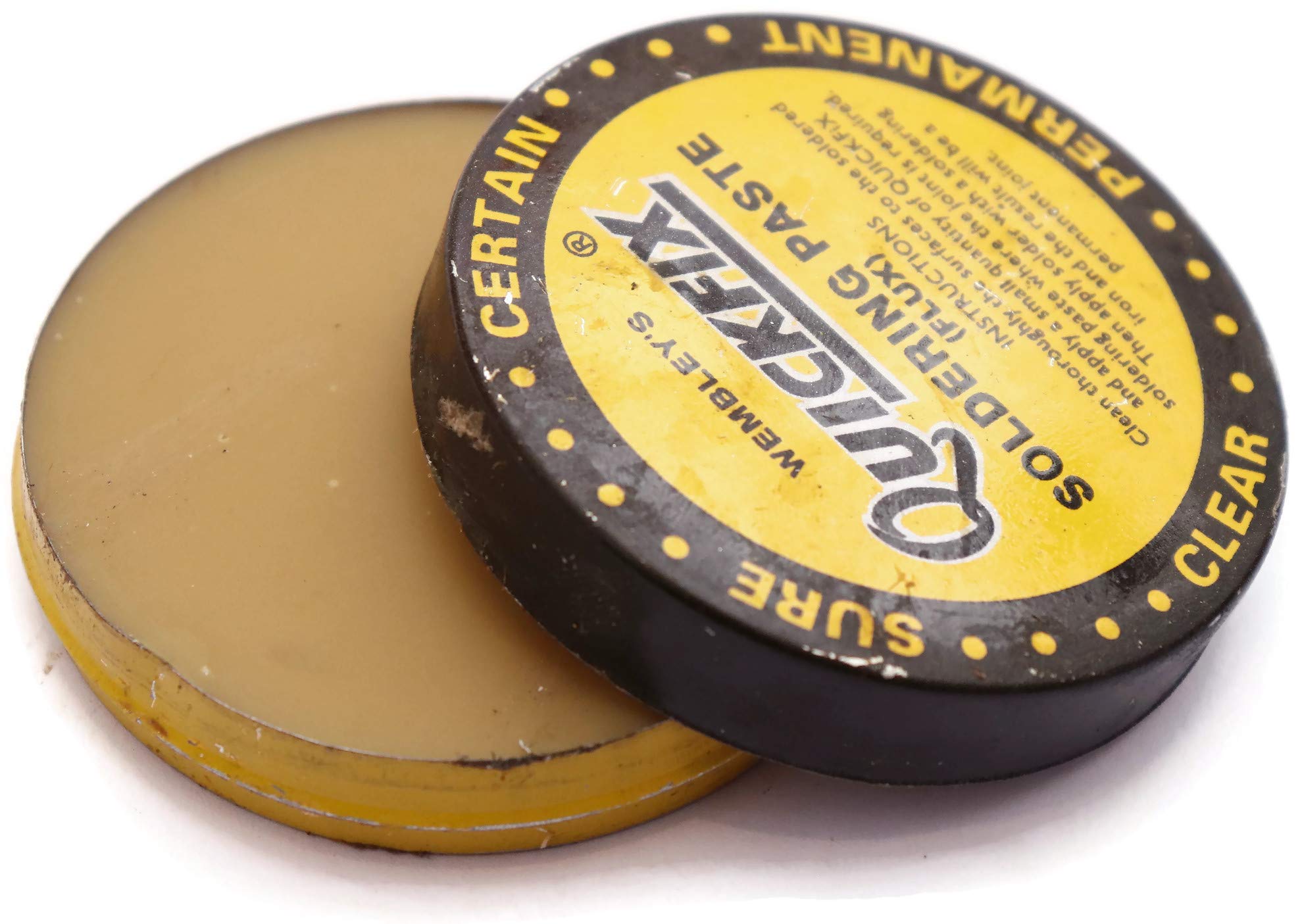
Solder flux is a chemical cleaning agent that removes oxidation from metal surfaces before and during soldering. It helps solder flow smoothly, improves adhesion, and ensures a strong electrical connection. Without flux, solder joints may become weak or unreliable due to oxidation and impurities.

References: Reference,
Desoldering Vacuum Pump or Solder SuckerA desoldering vacuum pump, also known as a solder sucker, is a tool used to remove molten solder from circuit boards. It works by creating a quick suction force to pull away excess solder, making it easier to fix mistakes or replace components. This tool is essential for rework and repair in electronics.
References: Reference,
Group Assignment
Objective of the Group Assignment:
- characterize the design rules for your in-house PCB production process
- submit a PCB design to a board house
Individual Assignment
Objective of the Individual Assignment:
- make and test a microcontroller development board that you designed
The objective of this week's individual assignment is to make and test a microcontroller development board. For this, I did not design a new PCB; instead, I reused the one I created during the Electronics Design assignment. The PCB was designed using KiCad and features the ESP32-C3 microcontroller. I decided to use the same design for this week's Production assignment to proceed with fabrication. I have now started the milling process to produce the PCB, and the entire process is explained in detail below. Do you want to know how i design the PCB? Pleaseclick here.,
Converting the Gerber files to PNGs :
I copied my files to an external storage device like a pendrive, and then used the Fab Lab system to continue the remaining process, since all the required software for PCB milling is available on that system.
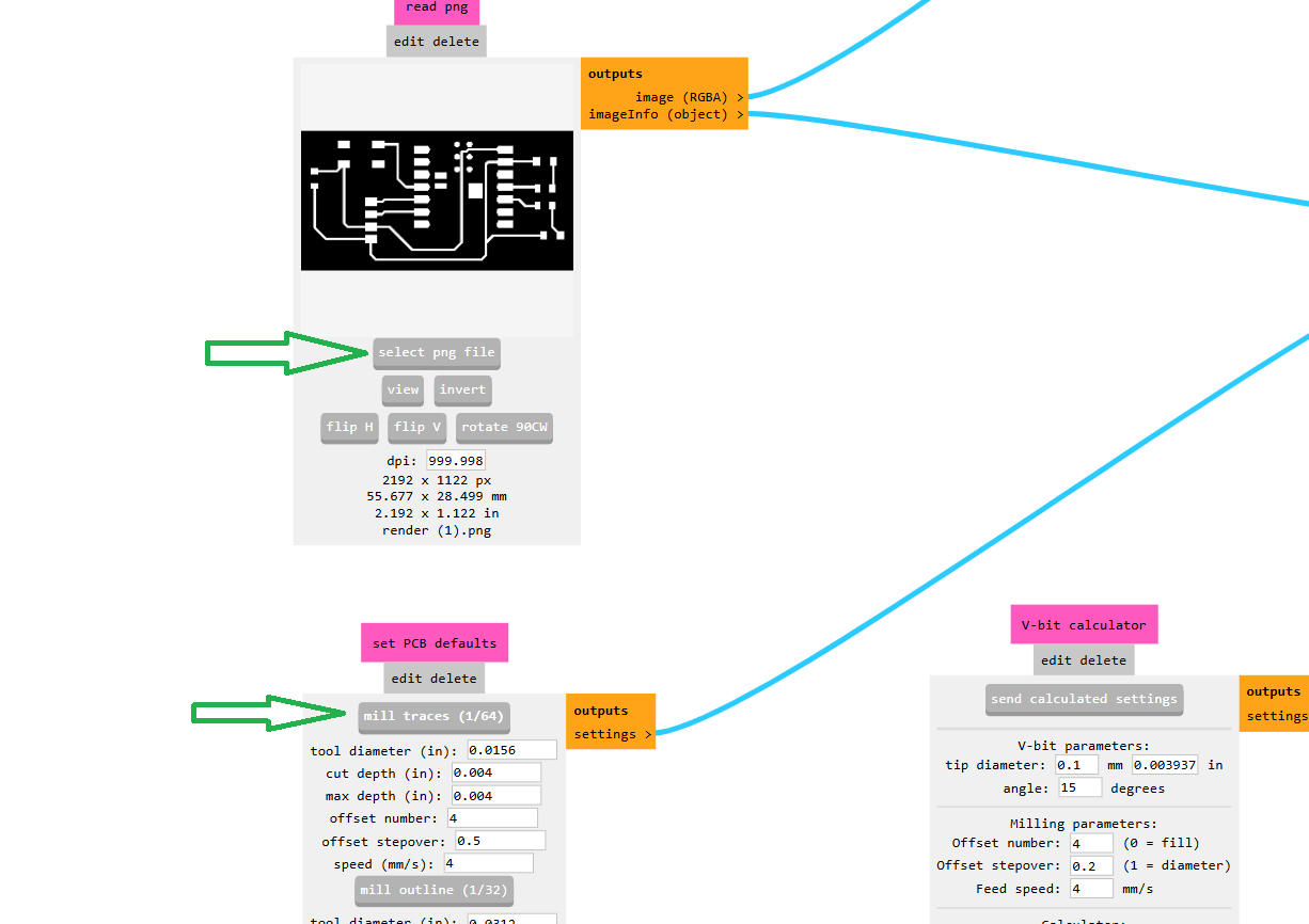
First, I converted the Gerber files into image format using the Gerber2Image online platform.
I converted both the trace cut and edge cut files.Do you want to visit the Gerber2Image platform?Click here
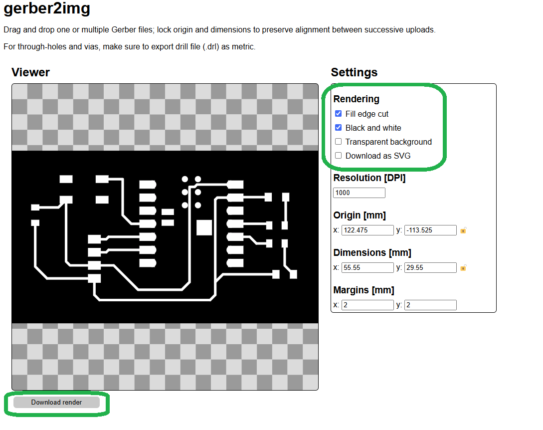
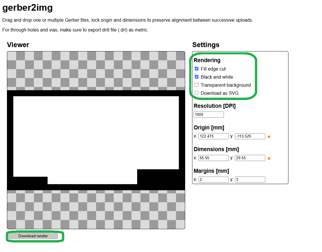
In the above image, I am showing how my trace cut and edge cut look after conversion. Once I confirmed everything was correct, I downloaded the rendered files by clicking on the "Download Render File" option.
Generating toolpaths using MODS CE :
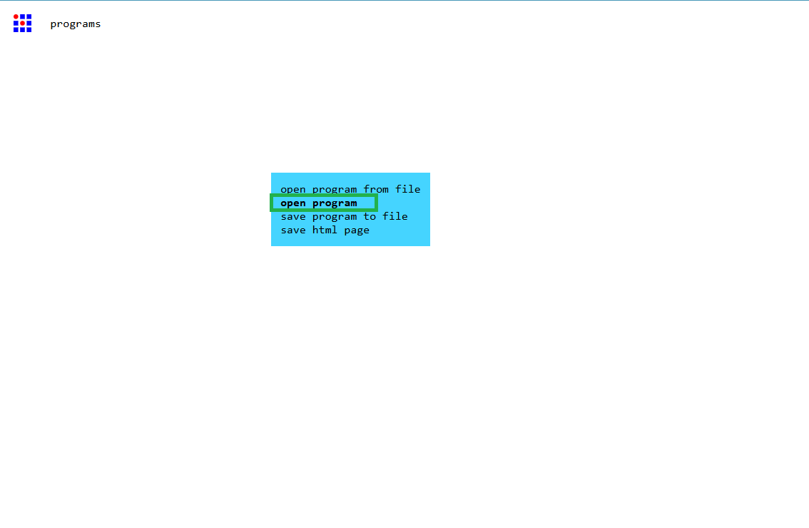
After that, I used Mods CE, an online platform designed for generating toolpaths from SVG files for PCB milling and other digital fabrication processes.
Mods CE allows users to convert design files into machine-readable formats, ensuring precise cutting and engraving.The image below shows the process of generating the toolpath using Mods CE.Do you want to visit the Mods CE platform?Click here

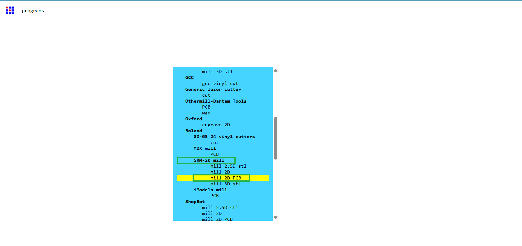
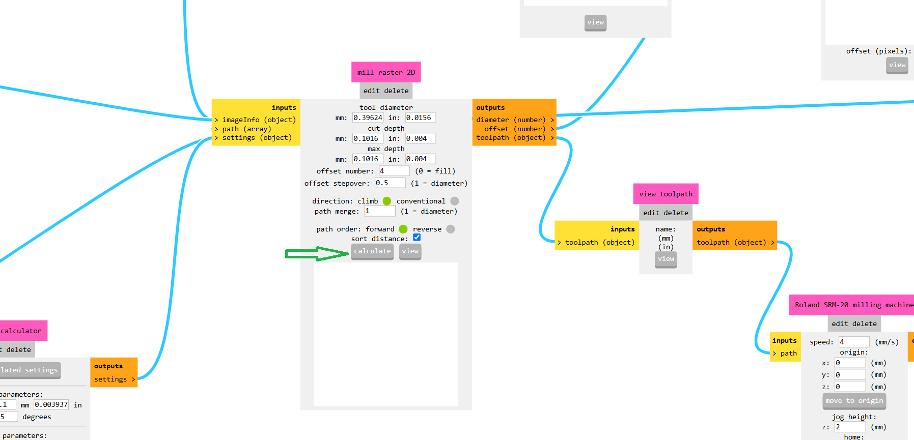
Here, I am using the SRM-20 mill, so I selected the 2D PCB milling option. Below, I am showing the interface of the Mods CE software.
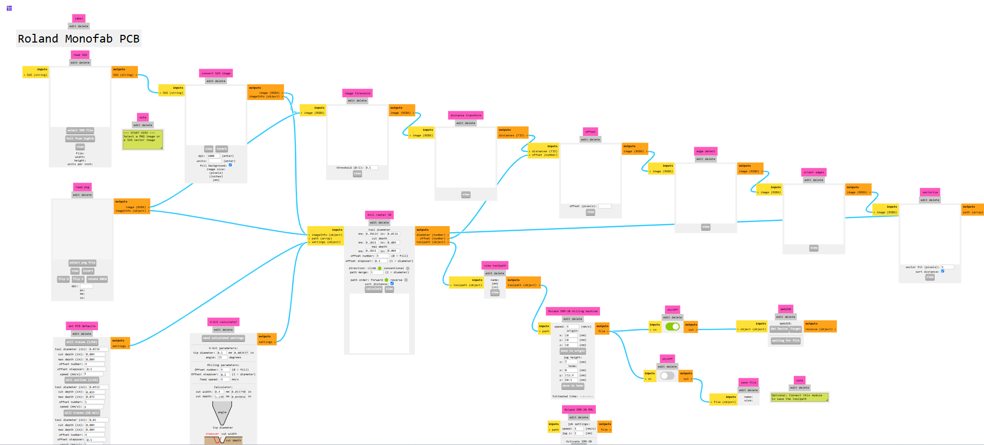
After that, I selected my PNG files which were previously downloaded from Gerber2Image. First, I selected the trace cut file, as shown in the image below.In the image below, I selected the 1/64 inch bit for my trace cut. After completing the process, I turned off the machine directly from the USB connection, as shown in the image.
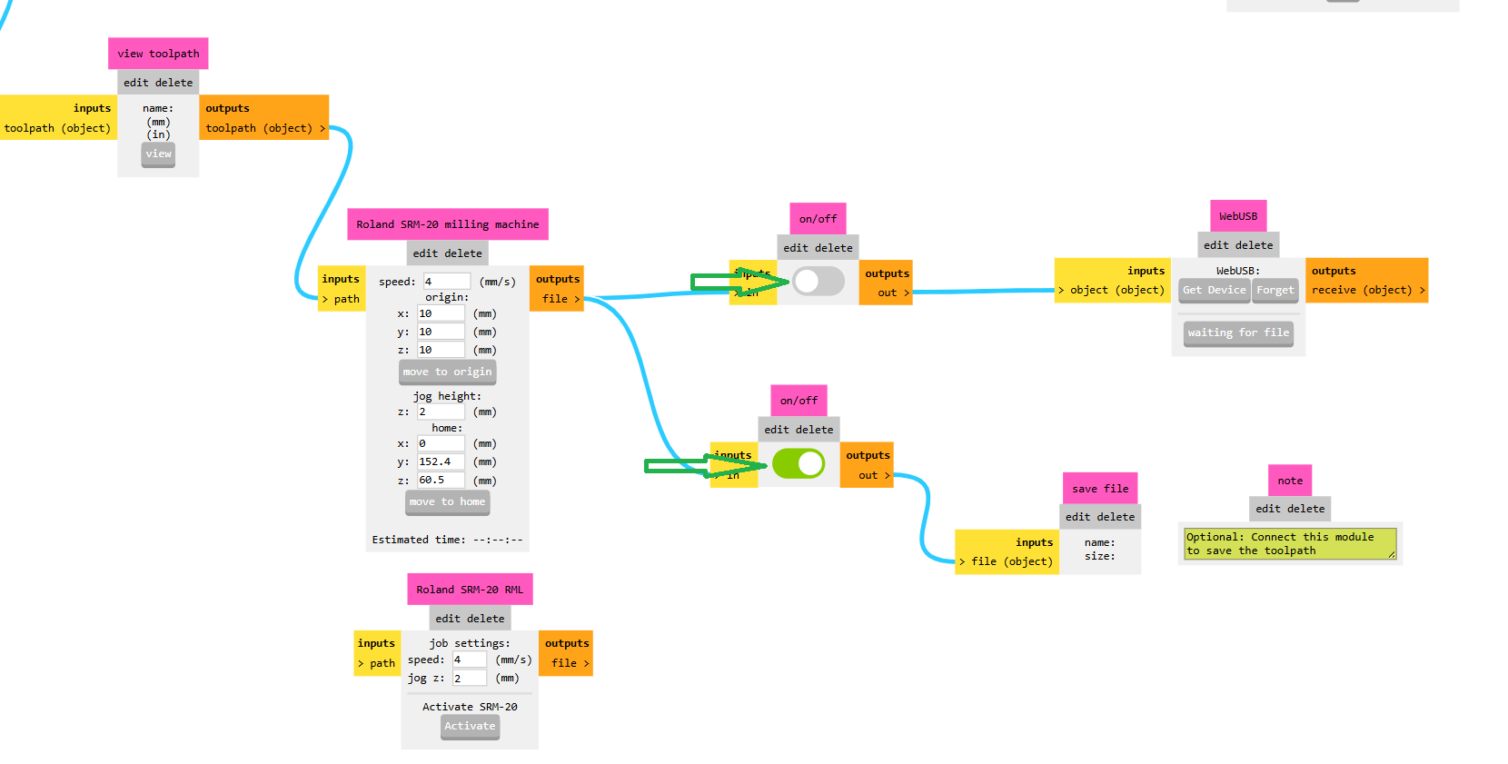
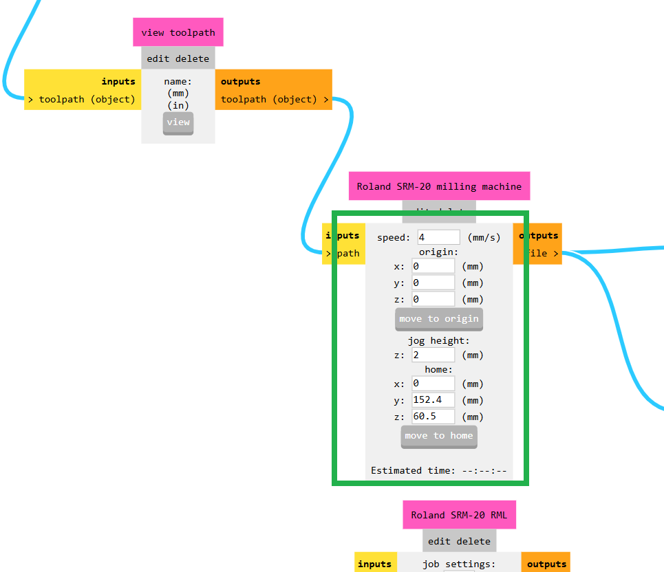
Then, I set the machine coordinates to (0, 0). After that, I downloaded the toolpath file to my PC, as shown in the image below.
I repeated the same process for the edge cut. For this, I selected the 1/32 inch bit to perform the cut.
Here, I am using VPanel software to operate the SRM-20 PCB milling machine.
PCB milling process :
VPanel is the control software used to operate Roland's SRM-20 milling machine. It allows users to set origin points, control spindle movement, and start or stop milling jobs.First, I opened the VPanel software and moved the machine tool to the correct position for PCB engraving, as shown in the image below.

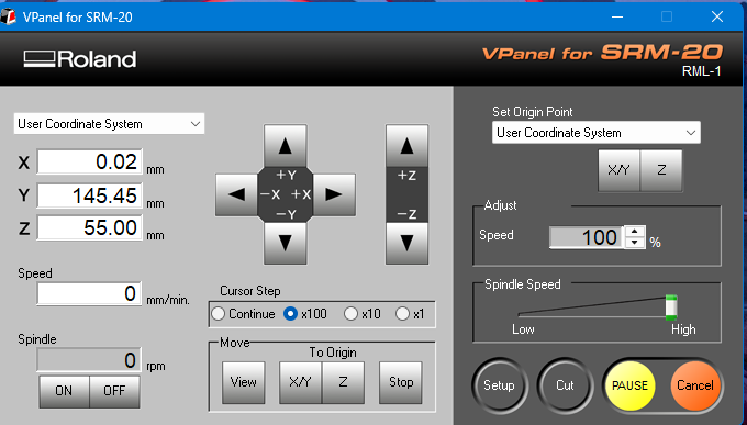
Before operating the machine, I cleaned everything inside the machine and then started moving the tool to position it for the engraving.
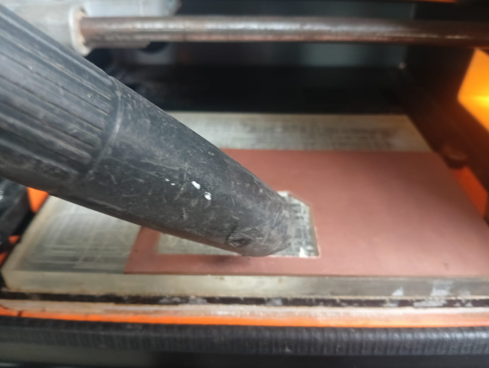
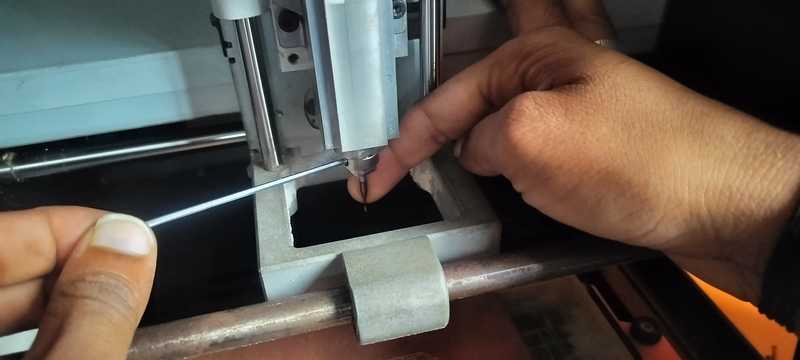
Before moving the tool, I fixed the 1/64 inch bit to the machine and then started moving the tool to the desired position.
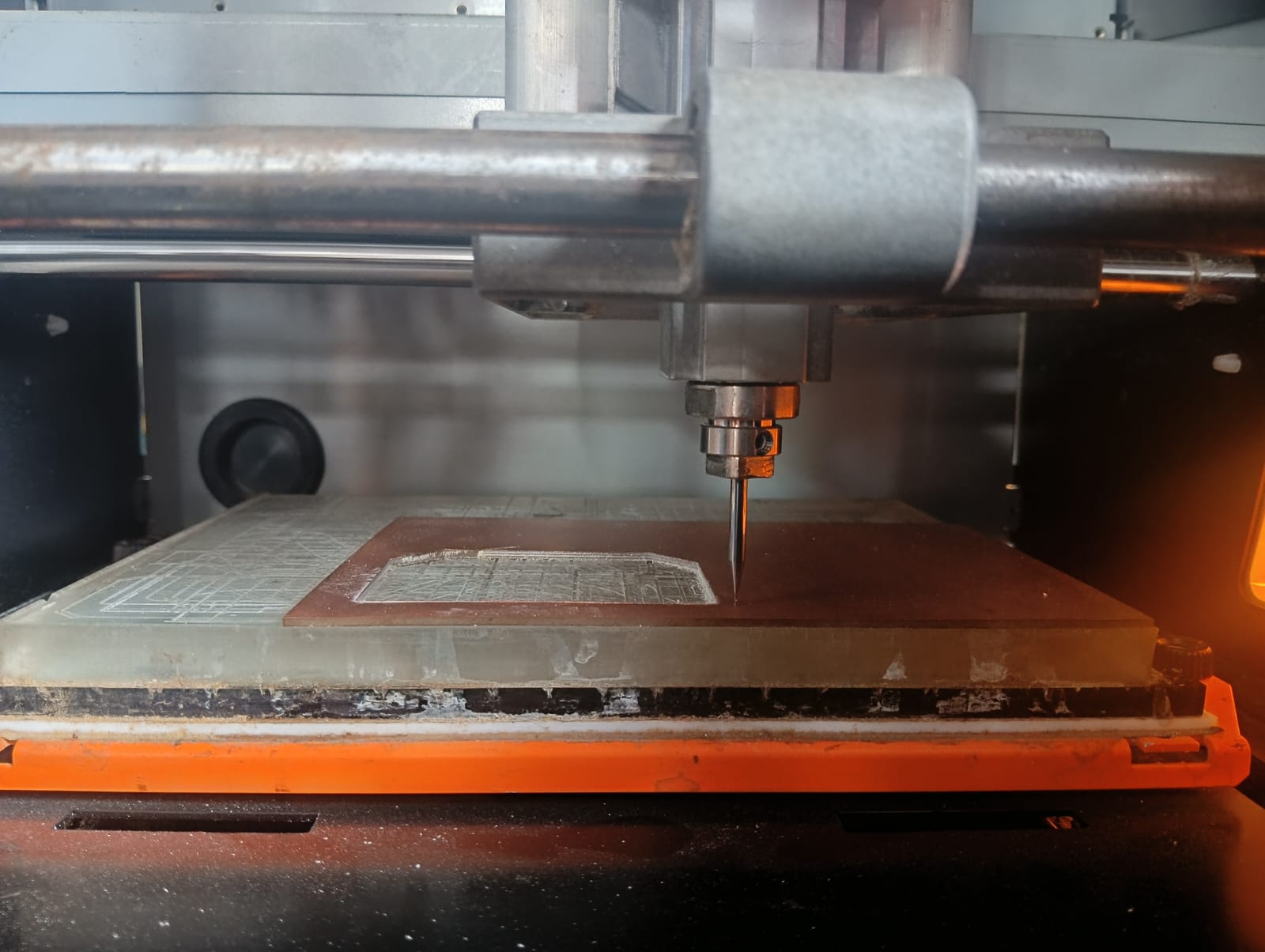
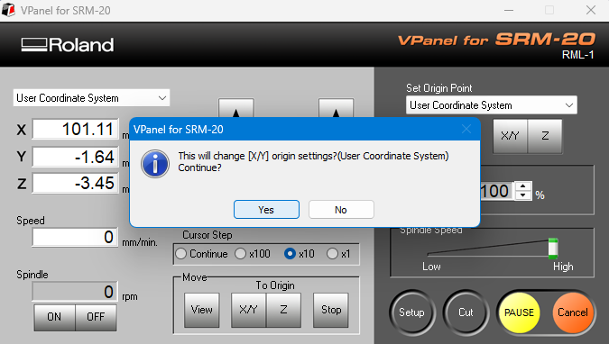
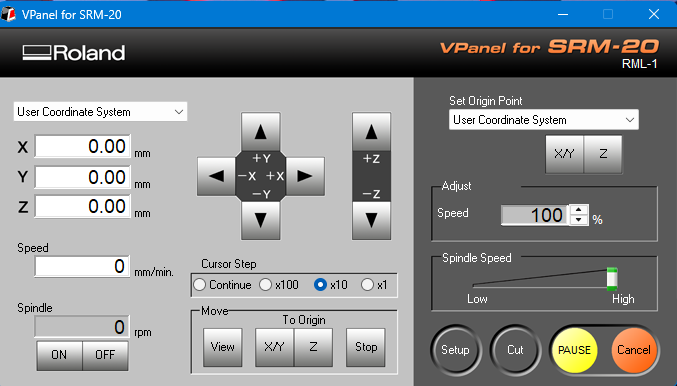
After moving the tool bit into the PCB engraving area, I set the (0, 0) coordinate in the VPanel software.
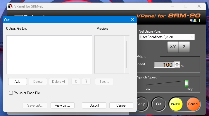
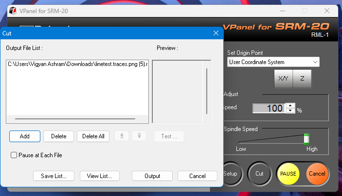
After that, I selected my file and started cutting the PCB. Below, I am showing how I selected the file and began the PCB cutting process.
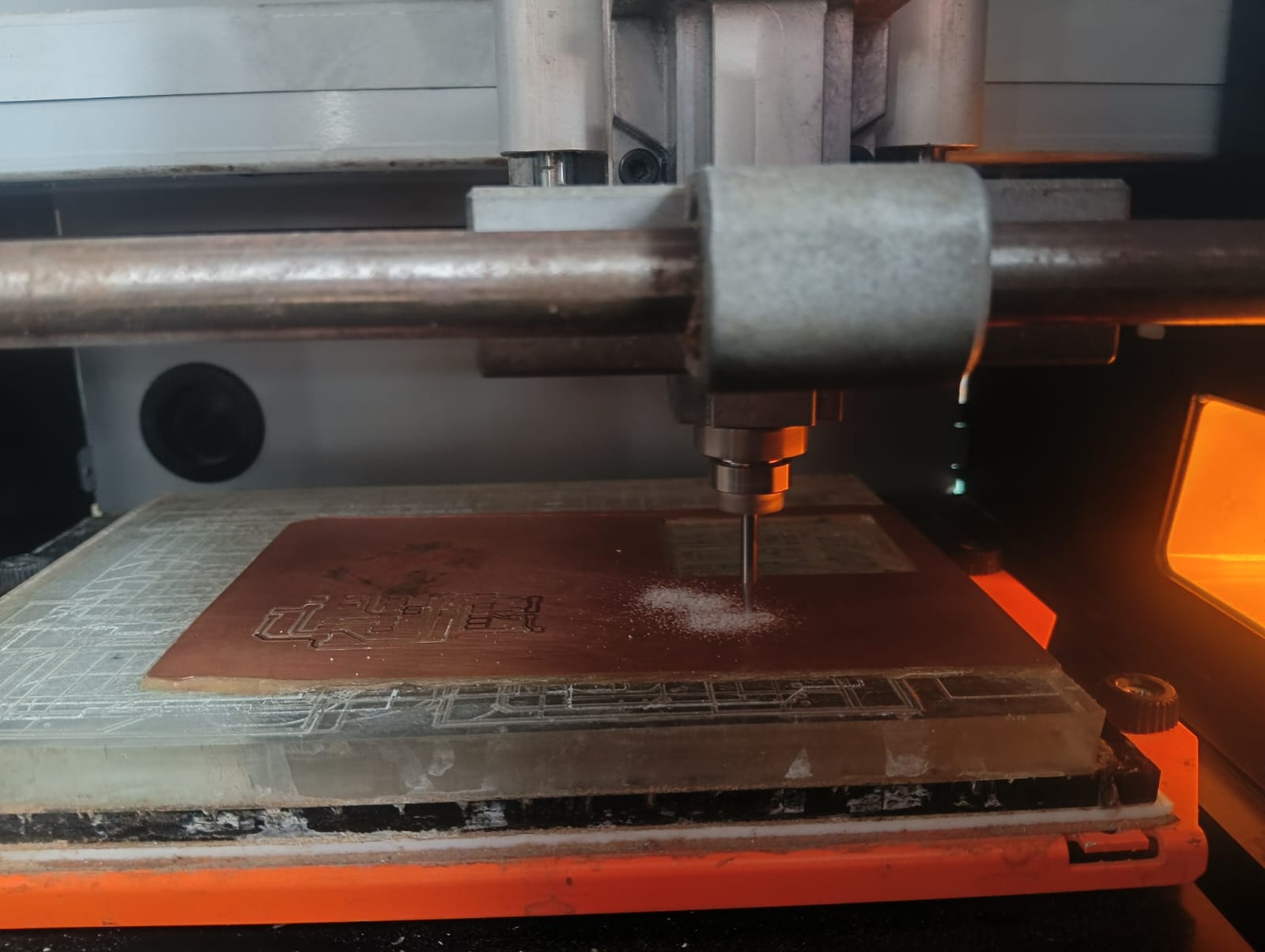
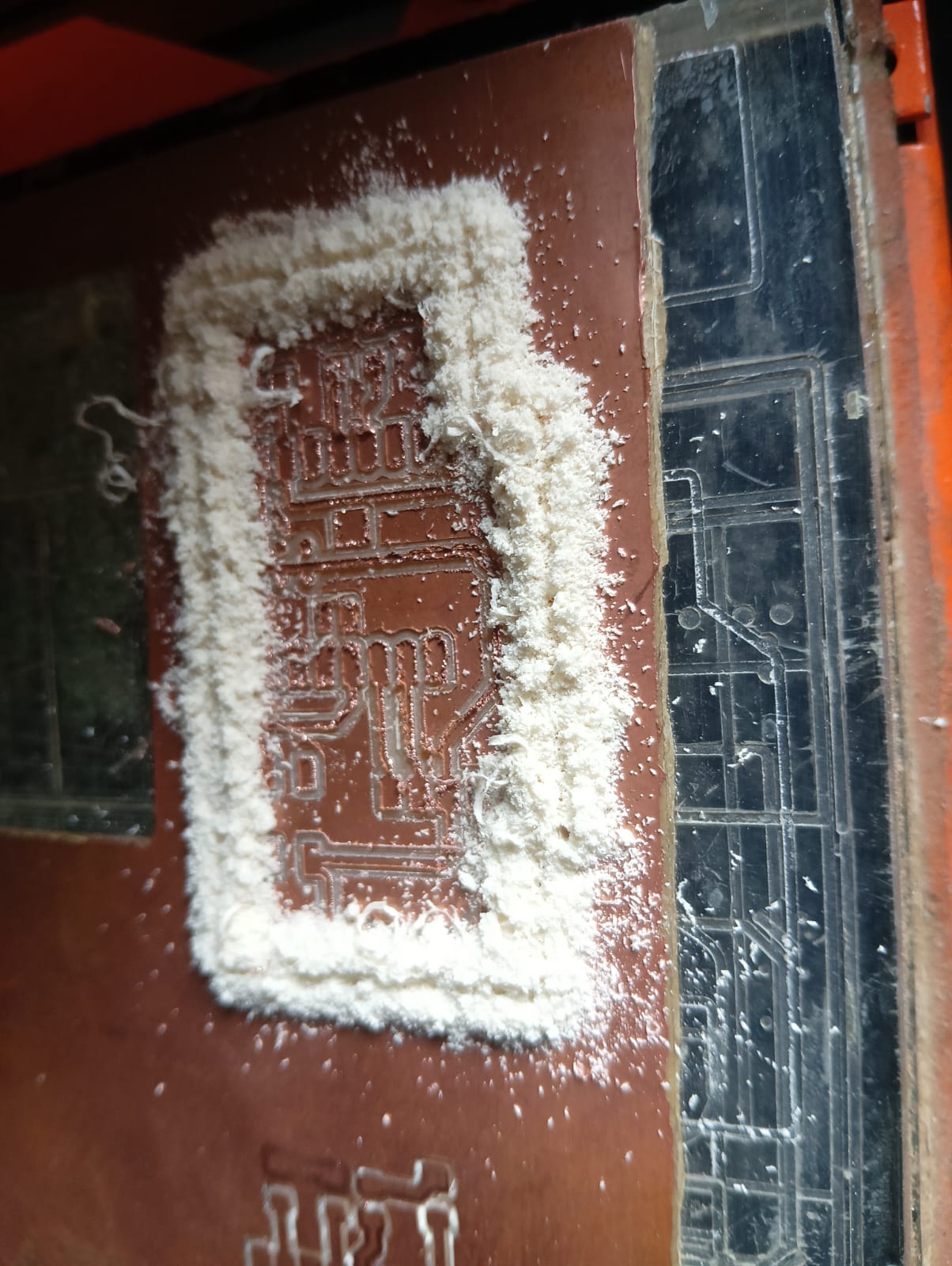
Below, I am showing the start of the milling process as my machine began cutting.
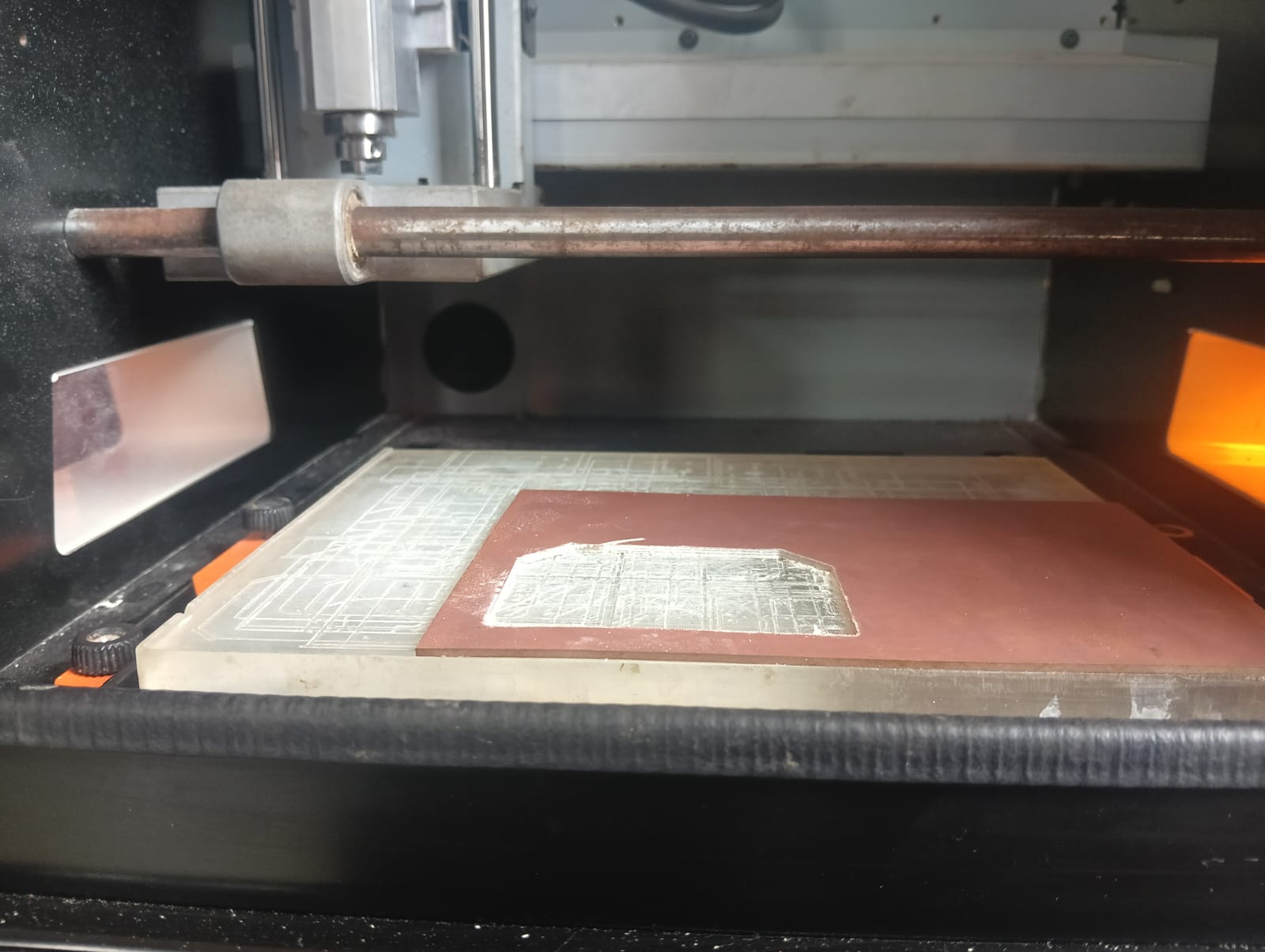
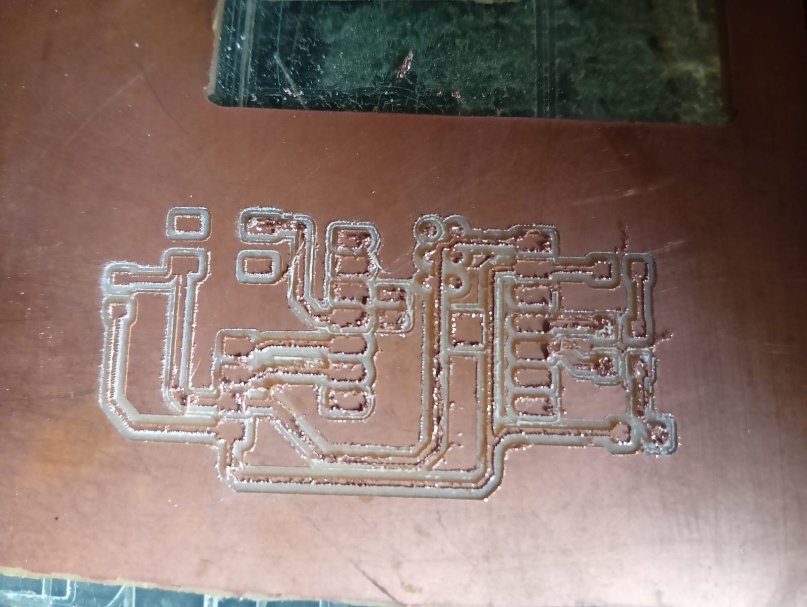
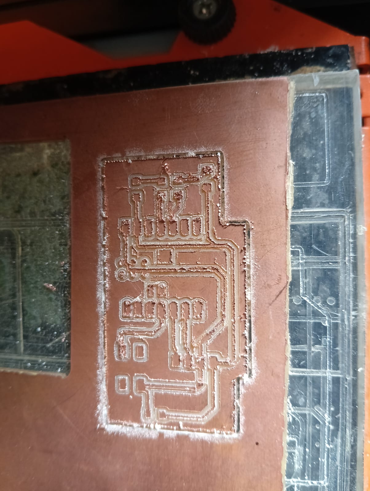
After completing the trace cut, I also show the final result of my PCB.
Use a sharp 1/64" tool bit for the trace cut to achieve precise and clean results. Accuracy improves when the tool is properly zeroed and the board is flat.
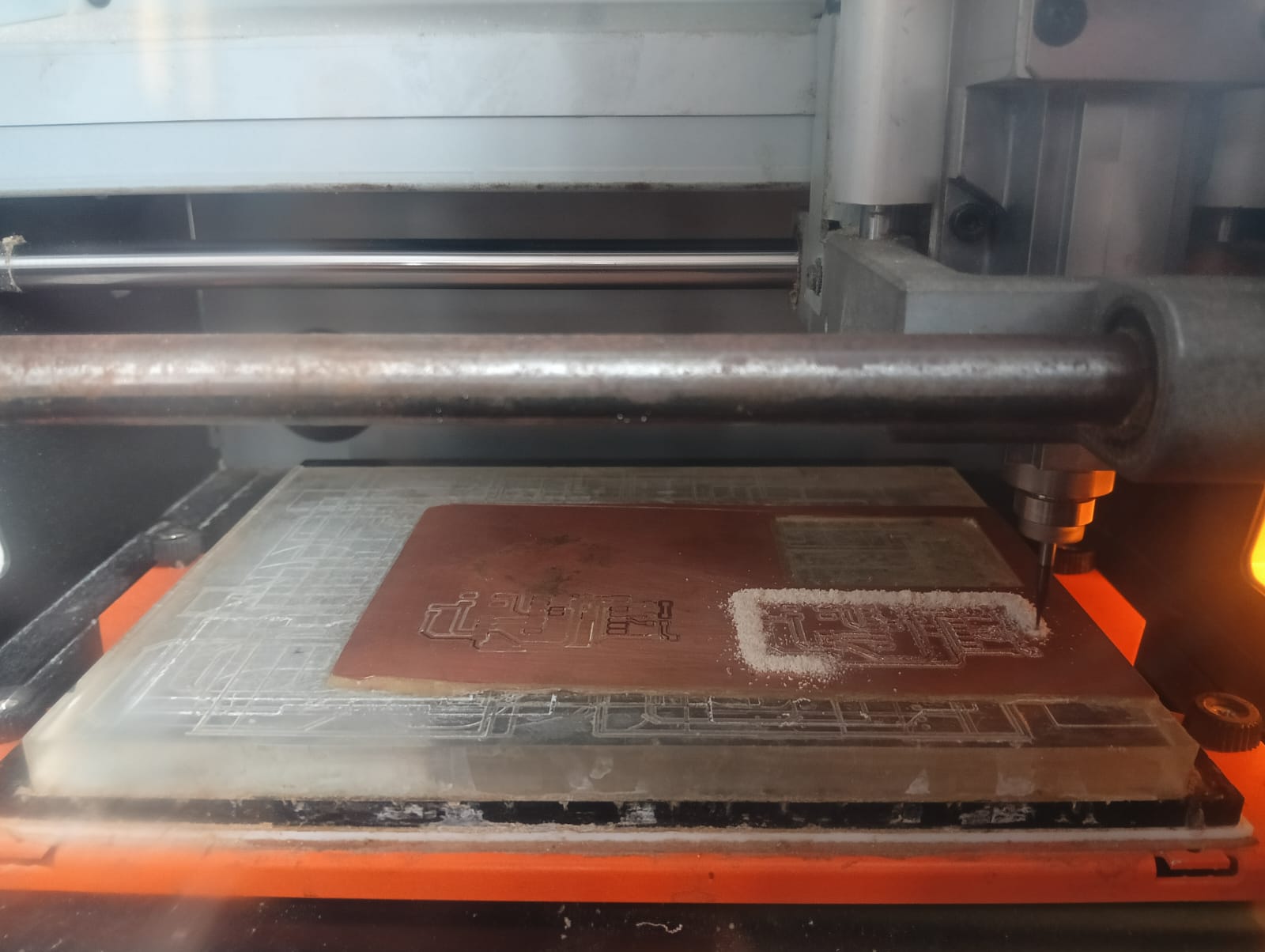
After completing the trace cut, I changed the bit to 1/32 inch for the edge cut. Then, I set the origin again to (0, 0), deleted the trace cut file, and selected the edge cut file to continue milling my PCB, as shown below.
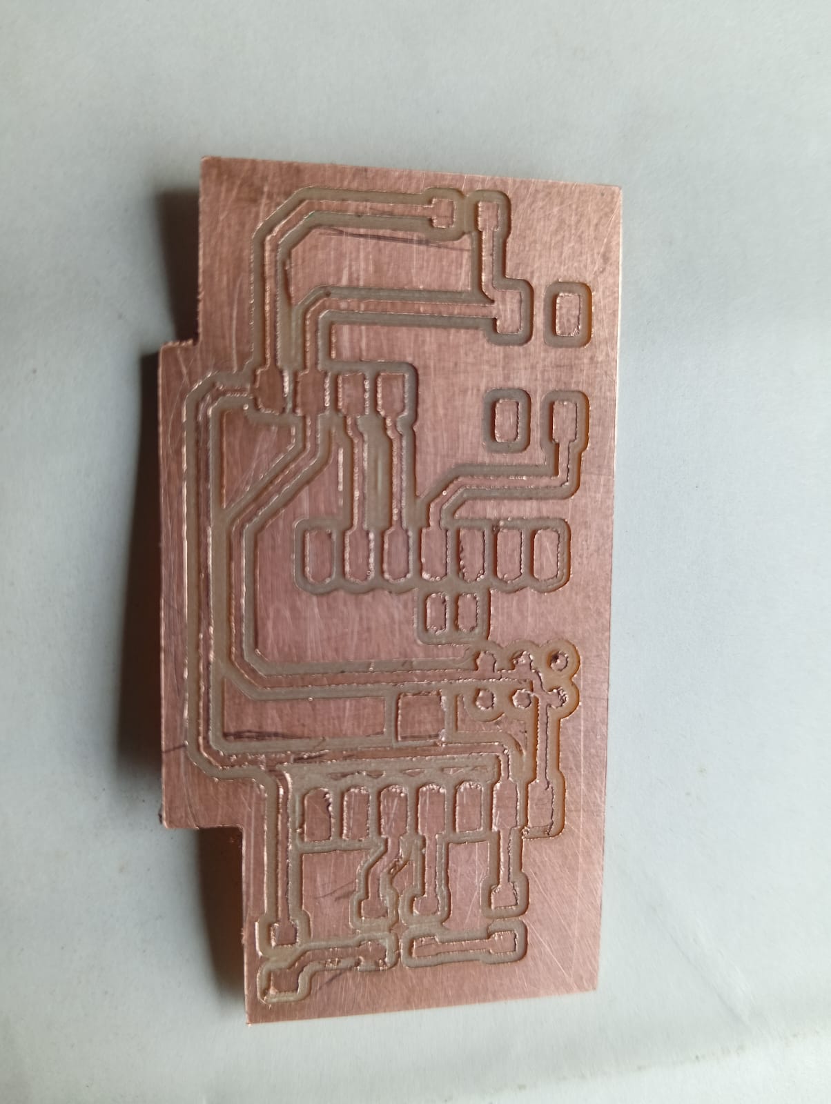
After completing the edge cut, I cleaned everything and turned off the machine. The final output of my PCB is shown in the image below.
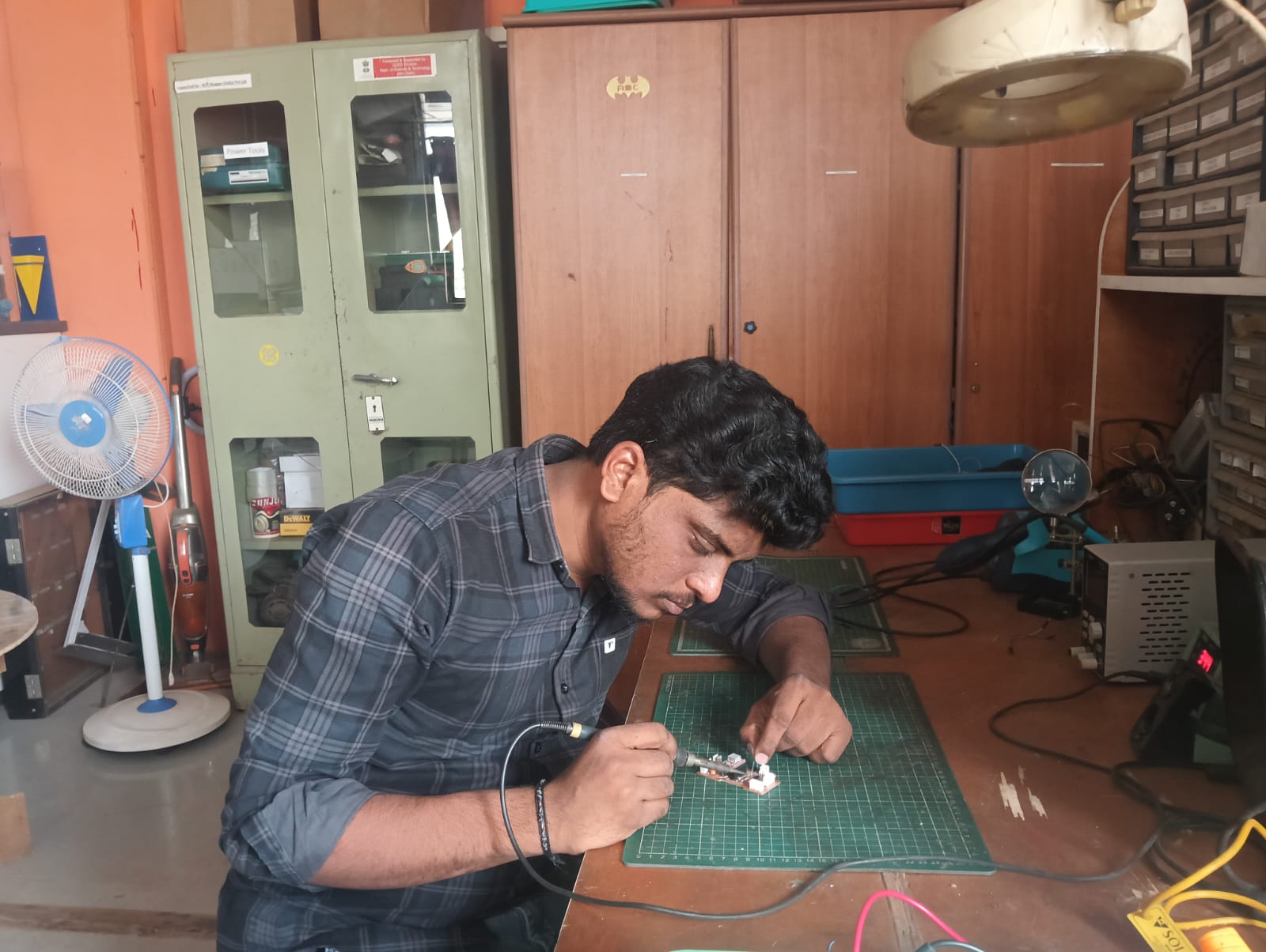
After completing the PCB cutting, I began soldering the components onto my PCB board.
Soldering is a crucial step to ensure proper connections between components and tracks.
Before explaining the process, I will describe the tools I used during soldering.
Below, I am showing the equipment used for component assembly and soldering.
These tools are essential for accurately placing and securely soldering the components onto the PCB.
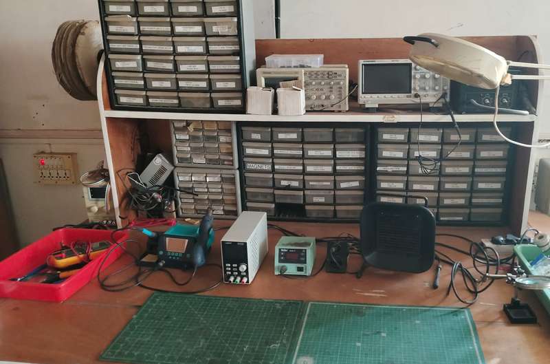
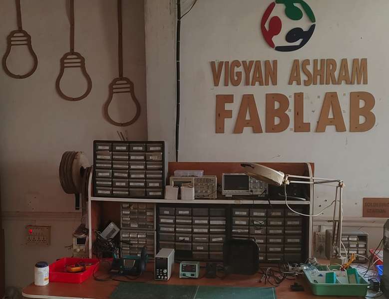
Below, I am showing the tools I used during the soldering process.
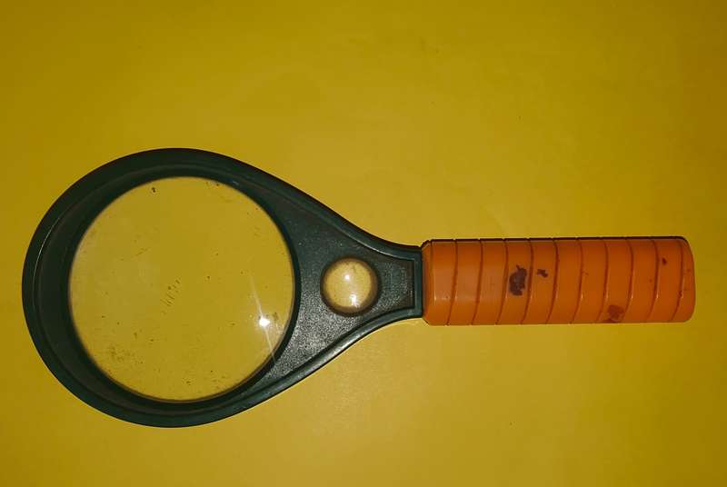
Magnifying Glass
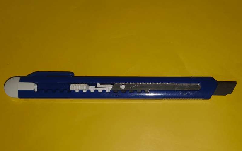
Knife
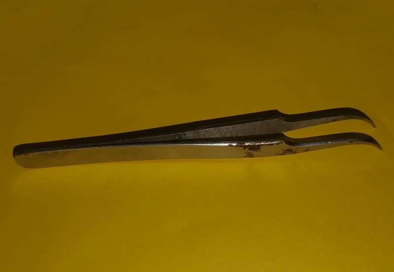
Curved Precision Tweezer
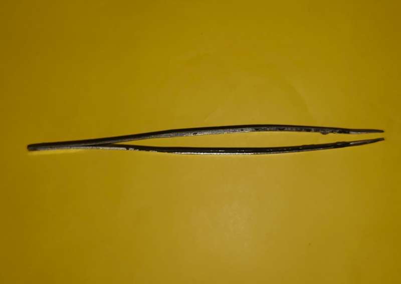
Straight Precision Tweezer
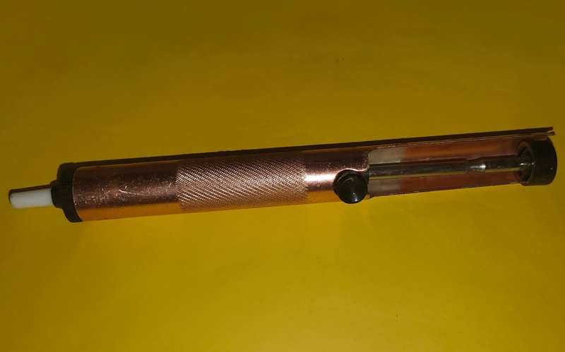
De-Soldering Pump
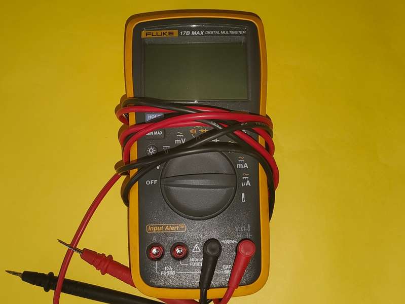
Multimeter
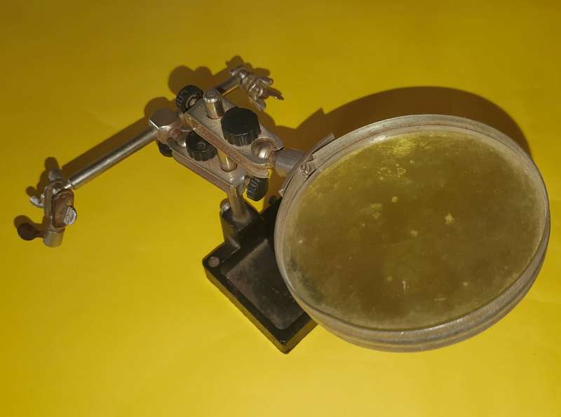
PCB Holder Magnifying Glass
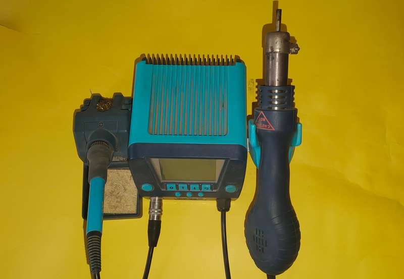
Soldering Iron
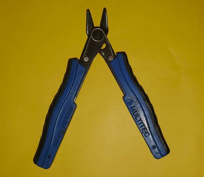
Wire Cutter
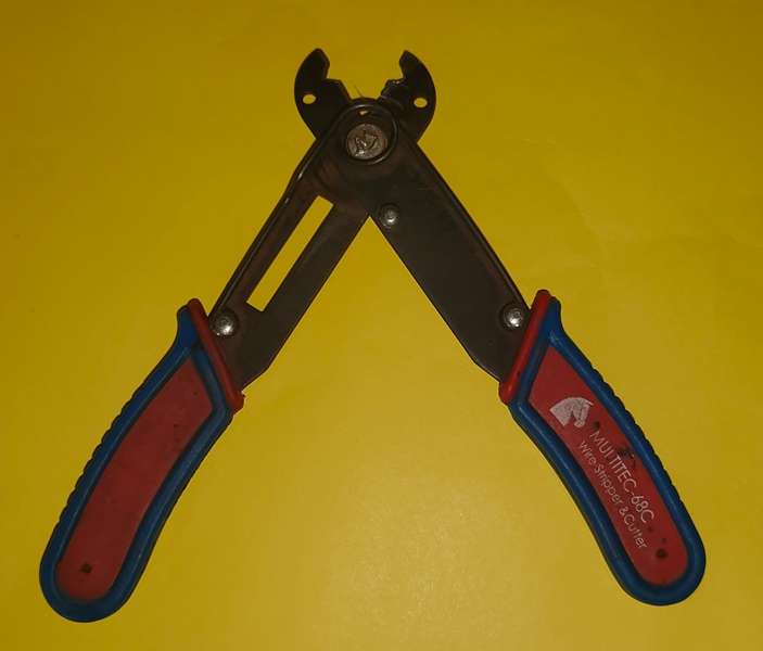
Wire Stripper
Soldering process
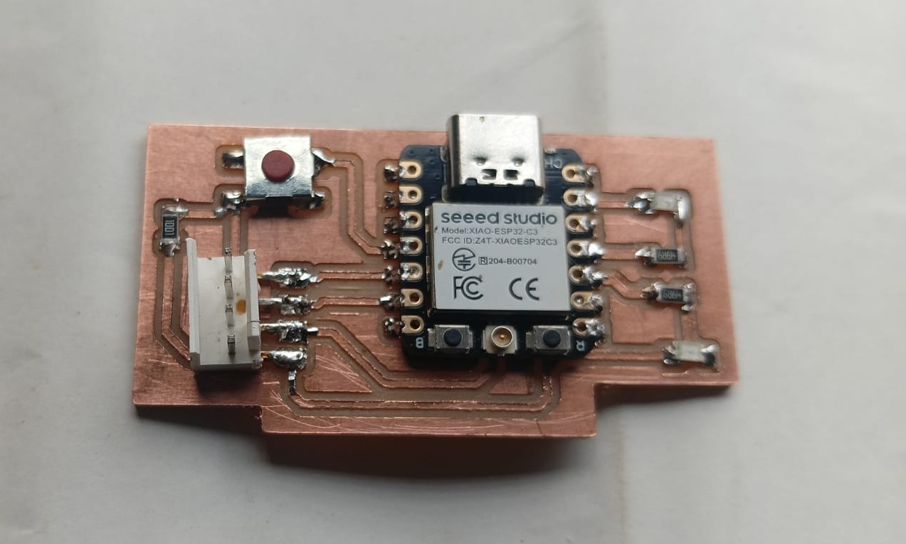
The components used in my PCB are listed below.
1. XAO ESP32-C3 Module
2. Omron Push Button Switch
3. SMD LED (Surface Mount Device LED)
4. Pin Header (1x4)
5. 1KΩ Resistor
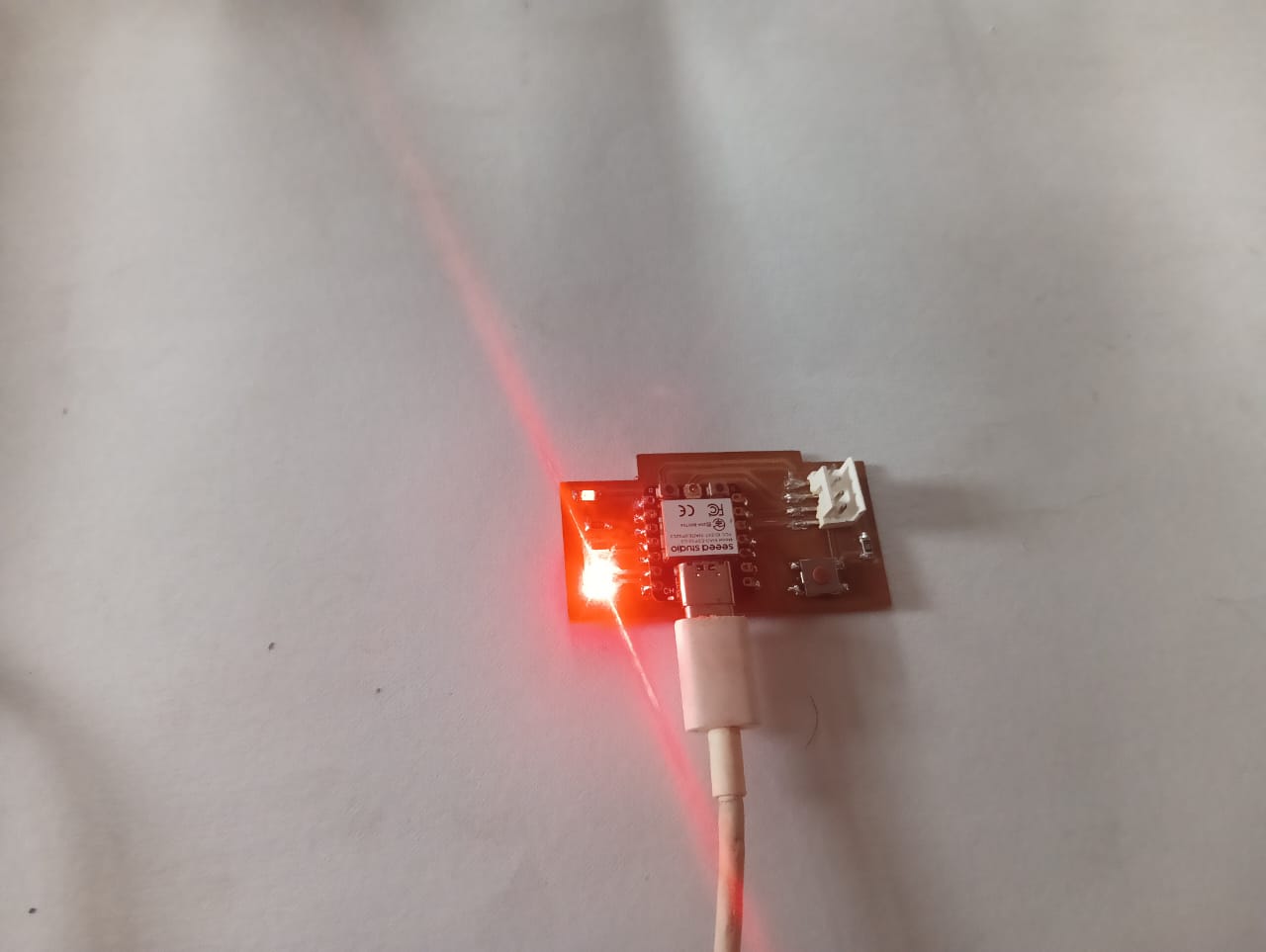
After preparing all the components, I began soldering them onto my PCB. The soldering process was done carefully to ensure proper connections and functionality. The final assembled PCB is shown below, fully ready for testing and use.
After completing the soldering, I proceeded to program my PCB board. I connected it to my PC using a USB cable and ensured proper communication between the board and the system. Once the connection was established, I started writing and uploading the code to the board.
Arduino Code for Controlling an LED
#define LED_PIN 10  // Change this to your connected LED pin

void setup() {
  Serial.begin(115200);    // Start serial communication
  pinMode(LED_PIN, OUTPUT);
  digitalWrite(LED_PIN, LOW);  // Ensure LED is off initially
}

void loop() {

      digitalWrite(LED_PIN, HIGH);
 delay(1000);
      digitalWrite(LED_PIN, LOW);
       delay(1000);

    }
  }
}
Positive Outcomes:
I am happy to share this week's positive outcome. This was my first hands-on experience with PCB milling using the SRM-20 machine. After completing the milling and holding my own PCB in my hand, I felt truly happy—there were no limits to my excitement. The moment I uploaded the code and saw the LED turn on was a next-level experience for me. It gave me a strong sense of achievement and motivation.
Challenges Encountered:
In this assignment, I faced a challenge during my first attempt at PCB milling—the traces were not cut properly. I repeated the same process but increased the depth of cut during toolpath generation. This small adjustment made a noticeable improvement. Although it wasn't a major issue, it helped me understand the importance of proper settings in PCB milling.