- Week 1 : Project Management
- Week 2 : Computer-aided
- Week 3 : Computer Controlled Cutting
- Week 4 : Embedded Programming
- Week 5 :3D Scanning and Printing
- Week 6 : Electronic Design
- Week 7 : Computer Controlled Machining
- Week 8 : Electronics Production
- Week 9 : Input Devices
- Week 10 : Output Devices
- Week 11 : Networking and Communication
- Week 12 : Mechanical Design and Machine Design
- Week 14 : Molding and Casting
- Week 15 : Interface and Application Programming
- Week 16 : System Integeration
- Week 17 : Wildcard Week
- Week 18 : Applications and Implications, Project Development
- Week 19 : Invention, Intellectual property and Income
- Week 20 : FInal Project Requirements
Week 6 : Electronic Design
This week describes my understanding of how to use KICAD for electronics design. It also includes how to create a project, how to draw a schematic, how to create a PCB layout, and how to export the Gerber files.
Objectives of the Week
Individual Assignment
- Use an EDA tool to design a development board.
- Interact with an electronic design workflow.
- Demonstrate schematic capture and PCB layout.
- Check design rules and manufacturing constraints.
- Export fabrication-ready design files.
Group Assignment Contribution
As part of the group assignment, I contributed to understanding the electronics design workflow and signal characterization process. I participated in observing and analyzing electrical signals generated by a microcontroller using measurement instruments such as a Digital Storage Oscilloscope (DSO) and a multimeter. This activity helped me understand the relationship between the designed electronic circuit and its real-world behavior, including voltage levels, PWM signal generation, waveform visualization, and basic signal validation. The experience provided valuable insights into testing and verifying electronic designs before fabrication and integration into larger systems.
View Group Assignment Documentation →
Electronic Design Automation (EDA) Tools
Electronic Design Automation (EDA) tools are software applications used to design, simulate, analyze, and validate electronic circuits and printed circuit boards (PCBs). These tools help engineers create schematics, assign component footprints, perform electrical verification, design PCB layouts, and generate manufacturing files required for fabrication.
EDA software plays a critical role in modern electronics development by reducing design errors, improving productivity, and enabling engineers to visualize circuits before physical manufacturing. Most EDA tools provide features such as schematic capture, PCB layout design, design rule checking (DRC), electrical rule checking (ERC), simulation, and 3D visualization.
Popular EDA Tools
| Software | Description | Platform |
|---|---|---|
| KiCad | Open-source EDA software widely used for schematic capture and PCB design. | Windows, Linux, macOS |
| EasyEDA | Cloud-based PCB design platform with integrated component libraries. | Web-Based |
| Altium Designer | Professional PCB design software used in industry. | Windows |
| Eagle | PCB design software from Autodesk. | Windows, Linux, macOS |
| OrCAD | Advanced electronic design suite used in commercial applications. | Windows |
Why KiCad?
For this week's assignment, I selected KiCad as my EDA tool. KiCad is a free and open-source electronic design automation suite that provides all the tools required for schematic capture, PCB layout design, 3D visualization, and manufacturing file generation. Because it is open-source and actively maintained by a large community, KiCad has become one of the most popular PCB design tools among students, makers, researchers, and professional engineers.
KiCad includes an integrated schematic editor, footprint manager, PCB editor, design rule checker, 3D viewer, and manufacturing file exporter. These capabilities make it an excellent platform for learning electronics design and PCB development.

Figure 1: KiCad main interface showing the available PCB design tools.
Major Features of KiCad
- Schematic Capture Editor
- PCB Layout Editor
- Electrical Rule Check (ERC)
- Design Rule Check (DRC)
- Footprint Management
- Integrated 3D Viewer
- Gerber and Manufacturing File Export
- Cross-platform Support (Windows, Linux, macOS)
- Open Source and Free to Use
Learning Resources
Before starting the PCB design workflow, I referred to KiCad documentation and beginner tutorials to understand schematic creation, footprint assignment, PCB routing, and design verification. These resources helped me become familiar with the complete electronic design workflow used throughout this assignment.
Reference Video: Complete KiCad Beginner Tutorial covering schematic design and PCB layout workflow.
Development Board Overview
For this assignment, I designed a custom development board based on the Seeed Studio XIAO ESP32-C3. The objective was to create a compact development platform that integrates power management, programming interface, input devices, and output devices while maintaining compatibility with in-house PCB fabrication processes.
The board was designed to support embedded programming assignments as well as future integration into larger projects. The design includes a XIAO ESP32-C3 module, user LEDs, push buttons, OLED display interface, and GPIO expansion headers.
Circuit Design and Component Selection
Before creating the PCB layout, the required components were selected based on the functional requirements of the development board.
| Component | Purpose |
|---|---|
| XIAO ESP32-C3 | Main microcontroller |
| Push Button | User input |
| LEDs | Status indication |
| Current Limiting Resistors | LED protection |
| OLED Header | Display interface |
| Pin Headers | GPIO expansion |
Schematic Explanation
The schematic was created using KiCad's schematic editor. The XIAO ESP32-C3 acts as the central controller and interfaces with all peripheral devices. GPIO pins were allocated for LEDs, push buttons, and communication interfaces. Power and ground connections were distributed throughout the design to ensure reliable operation.
Current limiting resistors were added in series with LEDs to prevent excessive current flow. Header pins were included to expose additional GPIO signals for future expansion and testing.
Components Used
| Component | Reference | Purpose |
|---|---|---|
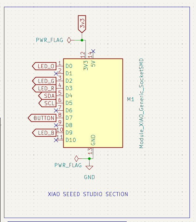
| Seeed Studio XIAO ESP32-C3 | M1 | Main microcontroller responsible for processing and communication. |
| Tactile Push Button | SW1 | User input for triggering events and testing digital inputs. |
| Pull-up Resistor (499Ω) | R1 | Maintains a stable logic level for the push button input. |
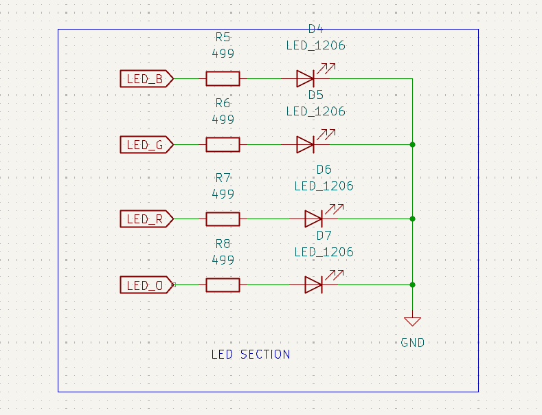
| LEDs | D4, D5, D6, D7 | Visual indicators for system status and GPIO testing. |
| Current Limiting Resistors (499Ω) | R5, R6, R7, R8 | Protect LEDs by limiting current flow. |
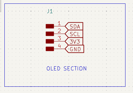
| OLED Display Header | J1 | Provides I2C connectivity for an external OLED display. |
| Power Flags | PWR_FLAG | Used to indicate valid power sources during ERC verification. |
| Power and Ground Symbols | 3V3, GND | Provide power distribution throughout the circuit. |
After importing and placing all required symbols, electrical connections were created using wires and net labels. This ensured that all components were properly connected to the XIAO ESP32-C3 and prepared for schematic verification through the Electrical Rules Check (ERC) process.
Creating a New KiCad Project
The first step in the electronics design workflow was creating a new project in KiCad. A project acts as a container that stores all design files, including the schematic, PCB layout, libraries, and manufacturing data. Creating a dedicated project helps organize the design process and keeps all related files in a single location.
After launching KiCad, I created a new project and selected a suitable project directory. KiCad automatically generated the project files required for schematic capture and PCB design. The project manager provides quick access to all design tools such as the Schematic Editor, PCB Editor, Footprint Editor, Gerber Viewer, and other utilities used throughout the development process.
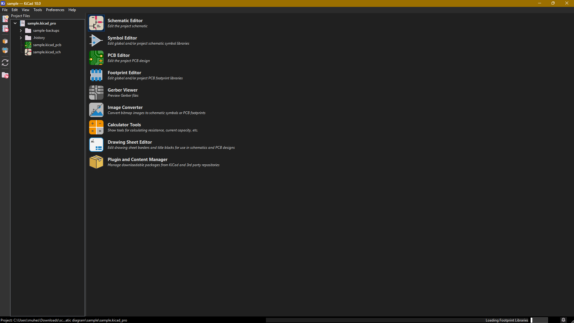
Figure: KiCad project manager showing the newly created project and available design tools.
Schematic Editor
The Schematic Editor is the starting point of the electronics design process in KiCad. It is used to create the electrical representation of the circuit by placing electronic components and connecting them using wires and nets. The schematic serves as a blueprint for the PCB design and defines how all components interact electrically.
Using the Schematic Editor, I added the required components for my development board, including the XIAO ESP32-C3 module, LEDs, resistors, push buttons, connectors, and communication interfaces. Each component was selected from the KiCad symbol libraries and positioned according to the intended circuit functionality.
Electrical connections were created using wires and net labels to ensure proper signal routing between components. Power symbols such as VCC and GND were also added to distribute power throughout the circuit. This approach helped keep the schematic organized and easy to understand.
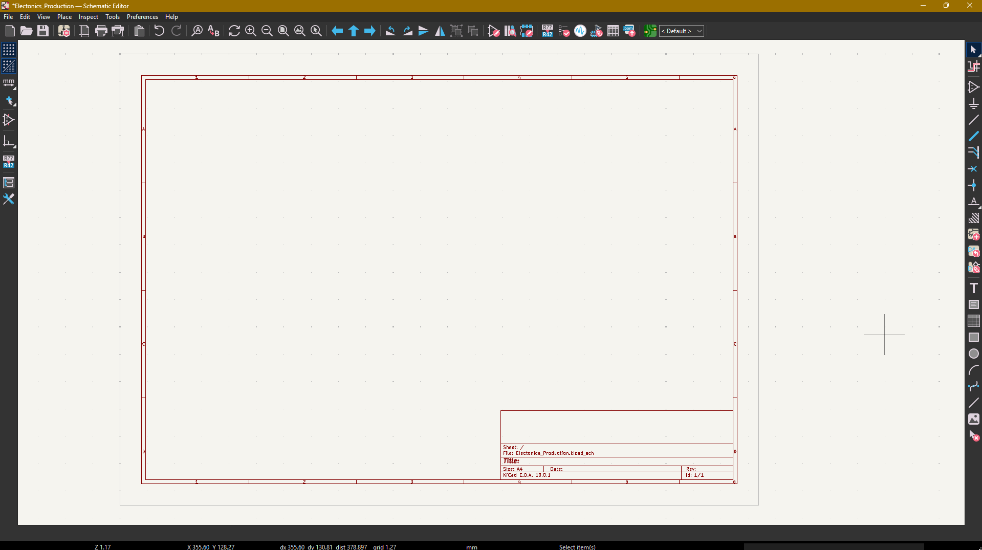
Figure: KiCad Schematic Editor used for creating the circuit diagram and establishing electrical connections between components.
Once the project was created successfully, I proceeded to the schematic editor to begin designing the circuit by selecting components, creating electrical connections, and defining the overall system architecture of the development board.
Fab Academy Electronics Library Installation
Fab Academy provides an official Electronics Library that contains schematic symbols and PCB footprints for components commonly available in Fab Labs. Installing this library simplifies the electronics design workflow by providing ready-to-use symbols and footprints that are compatible with the Fab Academy inventory.
The library was downloaded from the official Fab Cloud GitLab repository and imported into KiCad before starting the footprint assignment process.
Library Repository: https://gitlab.fabcloud.org/pub/libraries/electronics/kicad
Downloading the Fab Library
The Fab Academy Electronics Library was downloaded from the Fab Cloud GitLab repository. The package contains symbols, footprints, 3D models, documentation, and supporting resources required for electronics design in KiCad.
Figure: Downloaded Fab Academy Electronics Library repository containing symbols, footprints, 3D models, and supporting resources.
Installing the Symbol Library
To install the schematic symbols, KiCad's Symbol Library Manager was opened from the Preferences menu. A new library entry was created and linked to the fab.kicad_sym file located inside the symbols directory of the downloaded Fab Library.
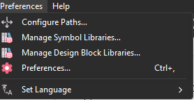
Figure: Opening the Symbol Library Manager from the KiCad Preferences menu.
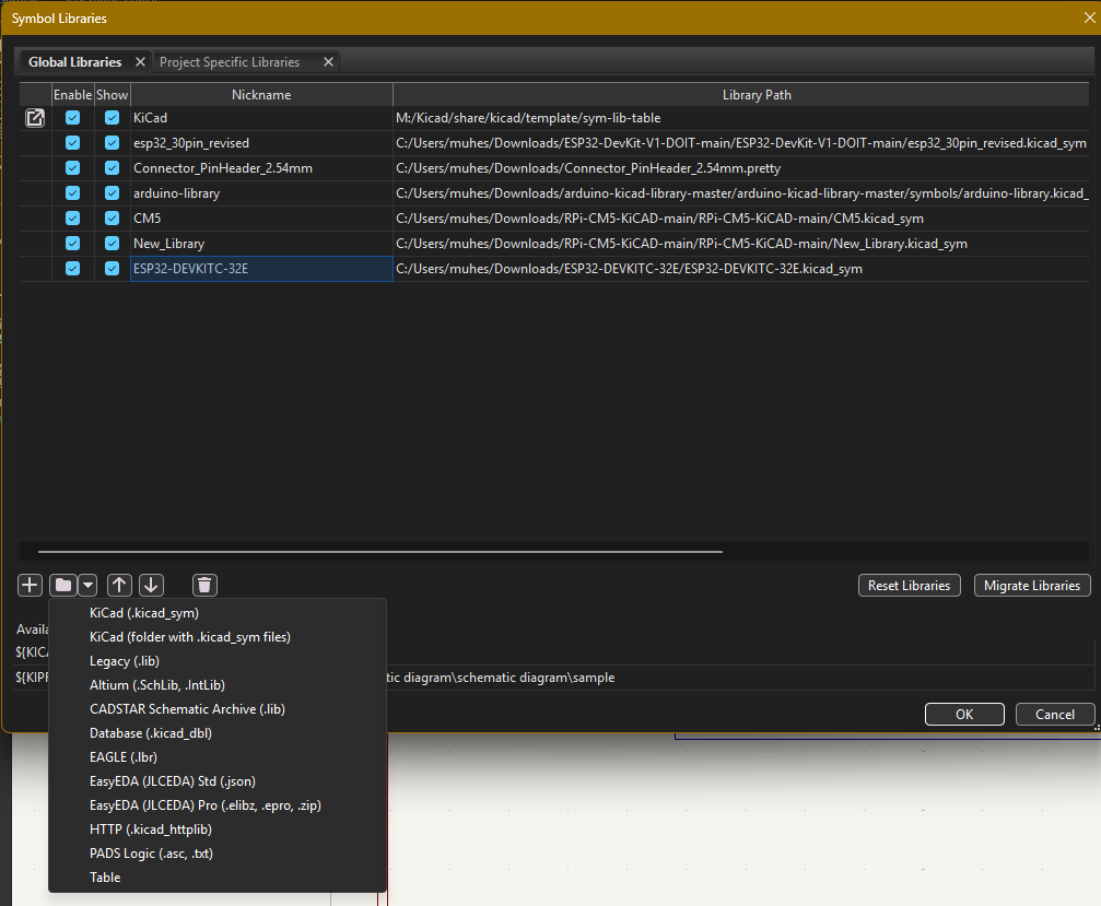
Figure: Creating a new symbol library entry.
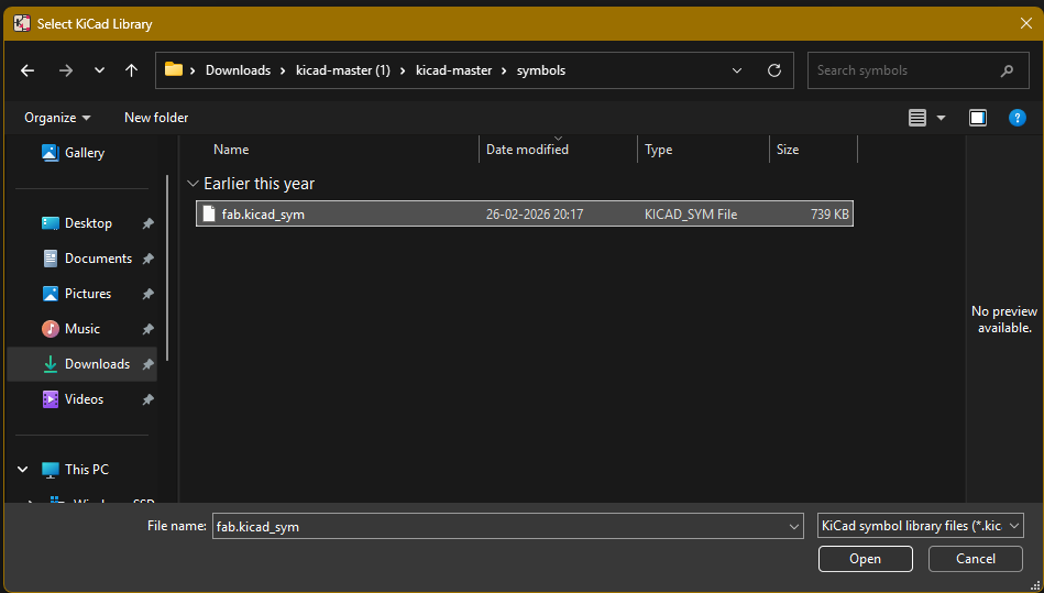
Figure: Selecting the fab.kicad_sym file from the downloaded library.
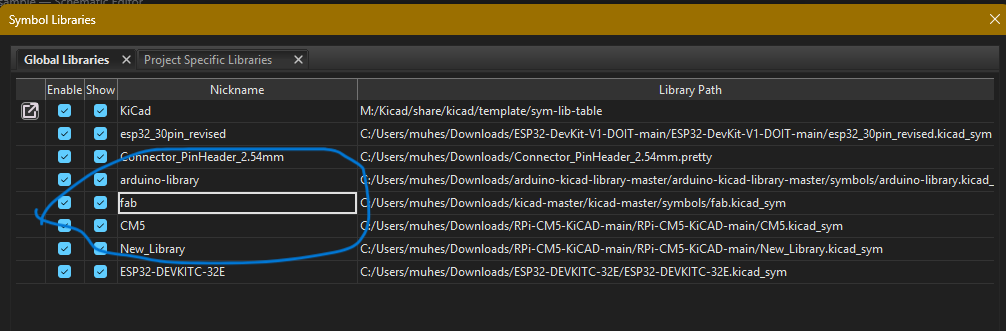
Figure: Fab symbol library successfully added to KiCad.
Installing the Footprint Library
After installing the symbol library, the Fab footprint library was added through the Footprint Library Manager. The footprint library contains the physical PCB packages required during PCB layout design.
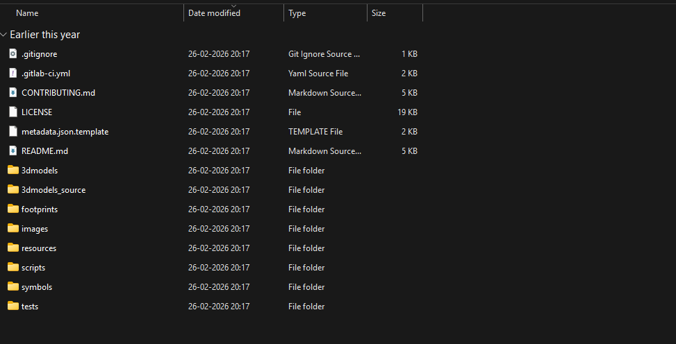
Figure: Opening the Footprint Library Manager from the Preferences menu.
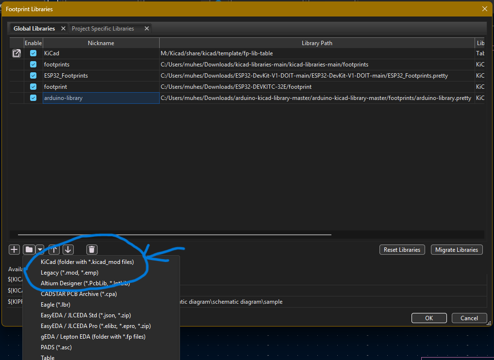
Figure: Creating a new footprint library entry.
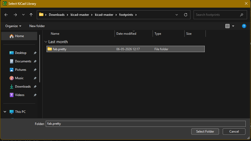
Figure: Selecting the fab.pretty footprint folder from the downloaded Fab Library.
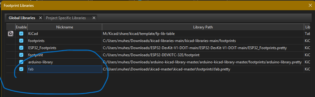
Figure: Fab footprint library successfully added to KiCad.
Benefits of Using the Fab Library
- Provides symbols and footprints for commonly used Fab Lab components.
- Reduces manual footprint assignment effort.
- Improves compatibility with in-house PCB fabrication workflows.
- Provides verified component packages for Fab Academy projects.
- Maintains consistency between student electronics designs.
- Includes both schematic symbols and PCB footprints in a single package.
After successfully installing both the symbol and footprint libraries, the components became available directly inside KiCad. The library was then used during the footprint assignment stage before transferring the design to the PCB Editor.
Importing Symbols and Component Selection
Before creating the schematic, the required electronic components were identified based on the functional requirements of the development board. KiCad provides an extensive symbol library that contains commonly used electronic components such as microcontrollers, resistors, LEDs, switches, connectors, and power symbols. These symbols can be imported directly into the schematic editor using the Add Symbol tool.
For this project, the required symbols were selected from the KiCad libraries and placed within the schematic editor. Each symbol represents an electronic component that will later be associated with a physical footprint during PCB design. The selected components were chosen to provide input functionality, output indication, communication interfaces, and power distribution for the development board.
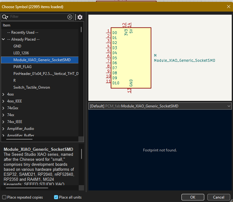
Figure: Selecting the Electronic components required from the Add Symbol tool.
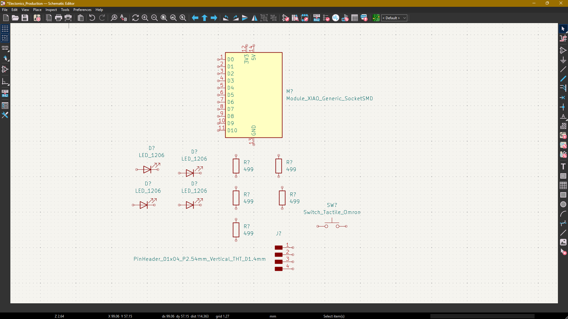
Figure: Components imported into the KiCad schematic editor for circuit development.
Using Global Labels and Signal Types
As the schematic becomes larger and more complex, directly connecting every component using wires can make the circuit difficult to read and manage. To simplify the schematic and improve readability, KiCad provides a feature called Global Labels. Global labels allow signals with the same name to be connected logically without requiring a physical wire connection across the schematic.
In this project, global labels were used to connect signals between the XIAO ESP32-C3, LEDs, push button, and OLED display interface. Signals such as LED_R, LED_G, LED_B, BUTTON, and SDA were assigned global labels so that the schematic remained clean and easy to understand.
Besides naming a signal, KiCad also allows the designer to define the electrical behavior of a label. A label can be configured as an Input, Output, Bidirectional, Passive, Tri-State, or Unspecified signal. These signal types are used by the Electrical Rules Checker (ERC) to verify that components are connected correctly and that no electrical conflicts exist within the design.
Creating Global Labels
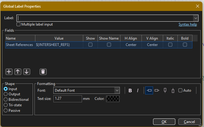
Figure: Global labels assigned to important signals such as LED outputs, button input, and OLED communication lines.
Global labels were placed on important signals to create logical connections across the schematic. Any signal sharing the same label name is automatically connected by KiCad, eliminating the need for long crossing wires and improving schematic organization.
Selecting Signal Types
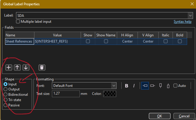
Figure: Global Label Properties window showing the available electrical signal types.
When creating a global label, KiCad allows the designer to specify the signal direction. These properties help ERC determine whether signals are connected correctly. Selecting the appropriate signal type improves design verification and helps identify wiring mistakes before PCB fabrication.
- Input: Signal enters the component.
- Output: Signal is generated by the component.
- Bidirectional: Signal can both send and receive data.
- Passive: Used for components that do not actively drive signals.
- Tri-State: Output can enter a high-impedance state.
Input and Output Signal Representation
Figure: Visual comparison between Input and Output global labels used within the schematic.
KiCad visually differentiates signal directions using the shape of the label symbol. Input labels indicate signals entering a component, while Output labels indicate signals generated by a component. For example, the BUTTON signal is configured as an input because the microcontroller reads the button state, whereas signals such as LED_R, LED_G, and LED_B are configured as outputs because the microcontroller drives the LEDs.
For communication interfaces such as I²C, signals like SDA and SCL are commonly configured as bidirectional because data can flow in both directions between the microcontroller and peripheral devices.
Organizing the Schematic into Functional Sections
After placing all the required components, the schematic was organized into functional blocks to improve readability and simplify debugging. As the number of components increases, a schematic can become difficult to understand if all components are placed together without structure. Dividing the design into logical sections makes it easier to identify signal flow and understand the purpose of each circuit block.
To achieve this organization, I used KiCad's graphical tools to create rectangular boundaries around related components. These boundaries visually separate the schematic into functional modules such as the microcontroller section, LED section, button section, and OLED interface section.
Drawing Section Boundaries
The rectangle drawing tool available in the schematic editor was used to create visual boundaries around groups of components. These rectangles do not affect the electrical functionality of the circuit but serve as documentation aids that improve the overall clarity of the design.
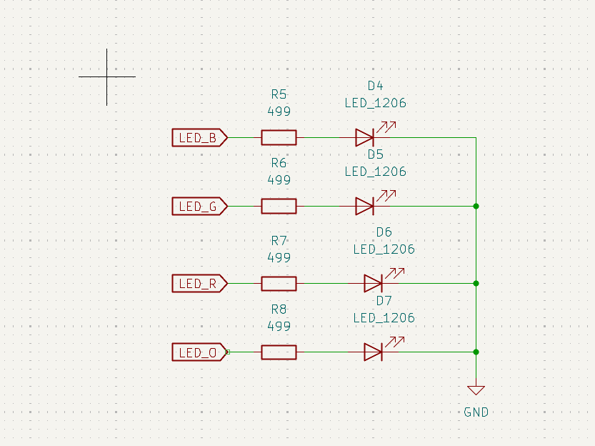
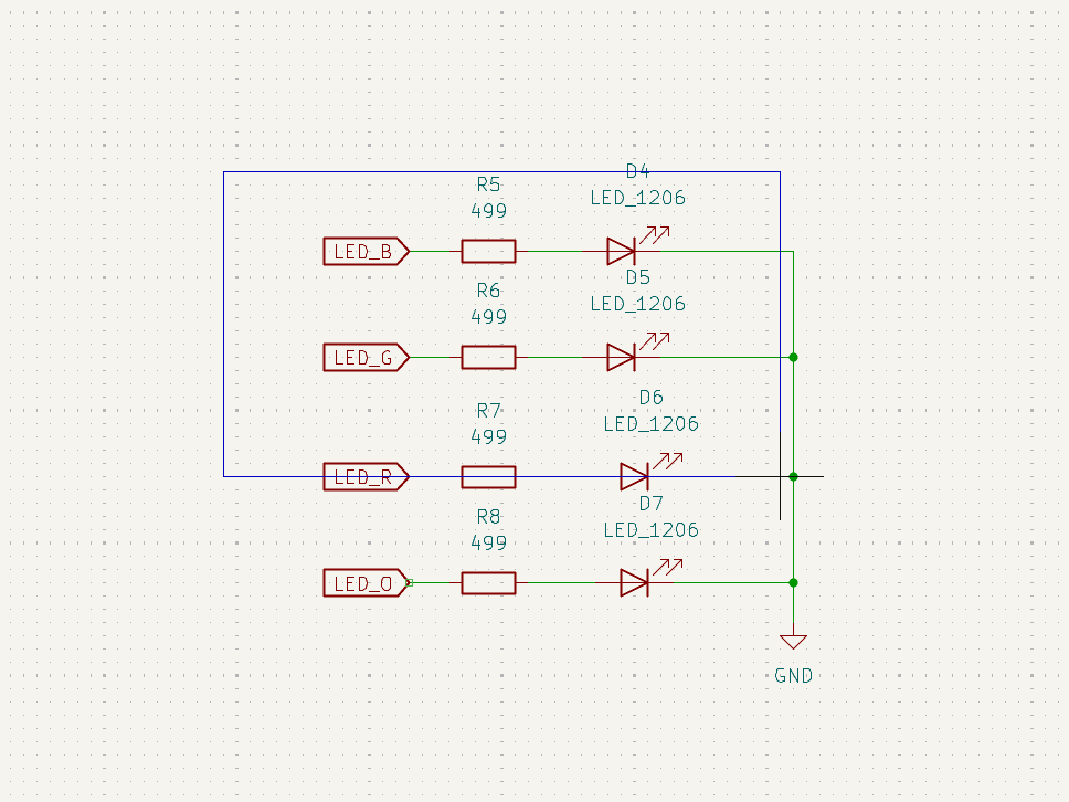
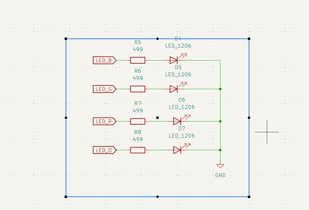
Figure: Using graphical rectangles to separate the schematic into functional blocks.
Adding Section Labels
After creating the boundaries, text labels were added using the text annotation tool. These labels identify the purpose of each section and make it easier for anyone reviewing the design to quickly understand the role of each circuit block.
Examples of section names used in this project include:
- Switch Section
- XIAO Seeed Studio Section
- LED Section
- OLED Section
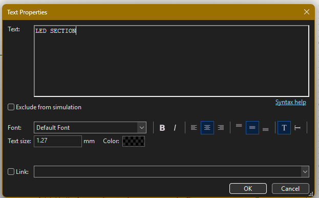
Figure: Text labels added to identify the functionality of each schematic block.
Once all boundaries and labels were added, the schematic became significantly easier to understand and navigate. Each functional block could be reviewed independently while still maintaining clear electrical connections through global labels and net connections. This structured approach improves documentation quality and simplifies future modifications to the design.
Final Organized Schematic
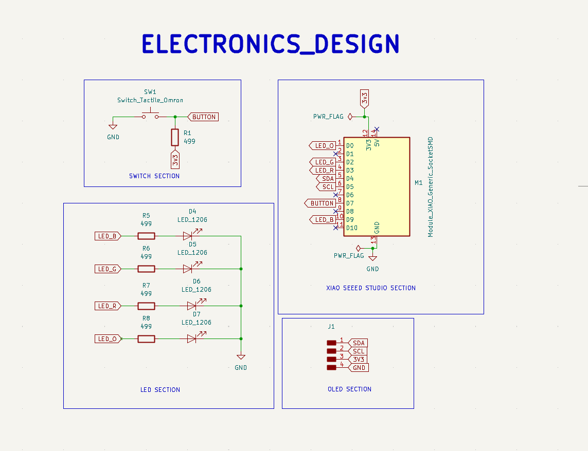
Figure: Final schematic organized into functional sections including the microcontroller, LED, switch, and OLED interface blocks.
Footprints Assigned in the Design
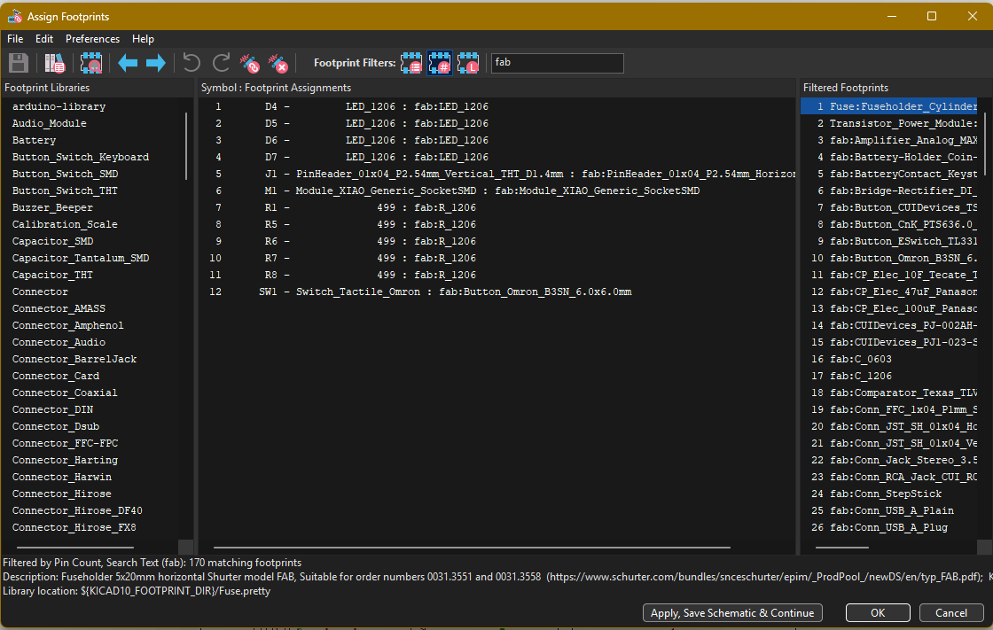
| Component | Reference | Assigned Footprint |
|---|---|---|
| XIAO ESP32-C3 | M1 | Seeed Studio XIAO ESP32-C3 Footprint |
| LEDs | D4, D5, D6, D7 | LED_1206_3216Metric |
| Resistors | R1, R5, R6, R7, R8 | R_1206_3216Metric |
| Push Button | SW1 | SW_SPST_EVQP7C |
| OLED Connector Header | J1 | PinHeader_1x04_P2.54mm |
After assigning all required footprints, the footprint associations were verified to ensure compatibility with the selected components and the in-house PCB fabrication process. This step ensured that every schematic component had a valid physical representation before transferring the design to the PCB Editor.
Annotating the Schematic
After completing the schematic connections, the next step was to annotate all components in the design. Annotation is the process of assigning unique reference identifiers to every component in the schematic. These reference numbers help distinguish components during circuit verification, PCB layout design, assembly, and debugging.
For example, resistors are assigned identifiers such as R1, R2, and R3, while LEDs are assigned identifiers such as D1, D2, and D3. Similarly, switches, connectors, and microcontrollers receive their own unique reference designators. These identifiers are automatically generated by KiCad using the annotation tool.
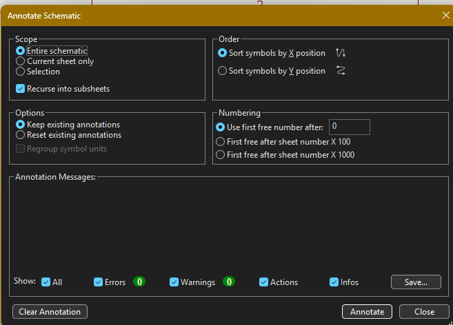
Figure: Annotation tool used to automatically assign unique reference numbers to schematic components.
Why Annotation is Required
- Assigns a unique identifier to every component.
- Prevents duplicate component references.
- Required before running ERC validation.
- Required before assigning footprints.
- Ensures proper synchronization between schematic and PCB layout.
- Facilitates component identification during assembly and debugging.
In this project, all components including the XIAO ESP32-C3 module, resistors, LEDs, push button, and OLED connector were automatically annotated using KiCad's annotation utility. After annotation, each component received a unique reference number and the schematic was ready for Electrical Rules Check (ERC) verification.
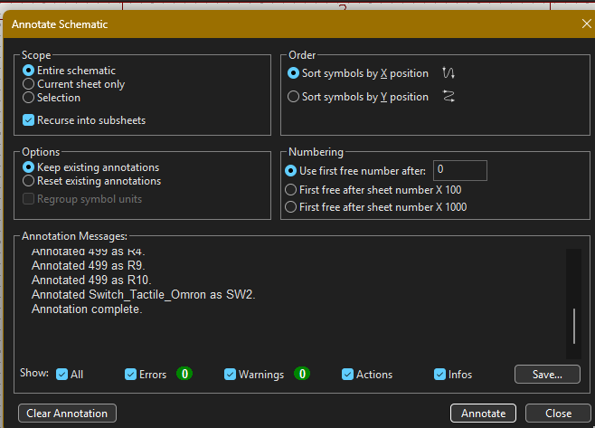
Figure: Fully annotated schematic showing unique reference identifiers assigned to all components.
Initial Electrical Rules Check (ERC)
After completing the schematic and annotating all components, an Electrical Rules Check (ERC) was performed. ERC is used to verify the electrical correctness of the schematic and identify potential design issues before proceeding to PCB design.
During the initial ERC verification, KiCad reported warnings related to the power nets. Although the circuit connections were correct, the software could not identify a valid power source driving the 3.3V and GND nets. As a result, ERC generated warnings indicating that the power inputs were not being driven.
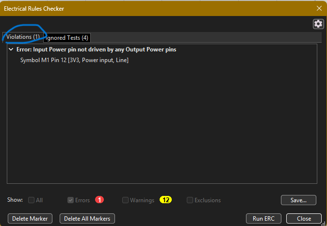
Figure: Initial ERC validation showing power-related warnings before adding Power Flags.
These warnings occurred because power symbols such as 3V3 and GND only identify power nets and do not indicate the actual source of power. To resolve these warnings, Power Flags were added to the schematic.
Using Power Flags for ERC Validation
During schematic design, KiCad performs an Electrical Rules Check (ERC) to verify that all electrical connections are valid. One common warning occurs when a power net is present in the design but KiCad cannot identify the source that is providing power to that net. Even though the circuit may be electrically correct, ERC may generate warnings indicating that the power input is not being driven.
To resolve this issue, KiCad provides a special symbol called PWR_FLAG. The Power Flag symbol informs the ERC engine that a particular net is intentionally powered and should be treated as a valid power source. This helps eliminate false ERC warnings and allows the design to pass validation successfully.
Why Power Flags Are Required
- Indicates that a power net is actively driven.
- Eliminates ERC warnings related to power connections.
- Helps KiCad correctly validate the schematic.
- Improves design verification before PCB fabrication.
- Ensures that power distribution is properly recognized by the software.
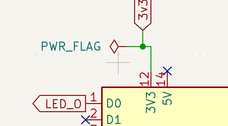
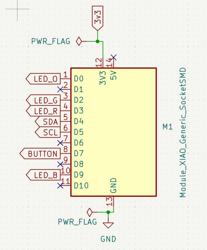
Figure: Power Flag symbols added to the 3.3V and GND nets to indicate valid power sources for ERC verification.
In this project, Power Flags were added to the 3.3V and GND nets connected to the XIAO ESP32-C3 module. These flags inform KiCad that the board receives power from a valid source and allow the ERC process to correctly validate the schematic without generating unnecessary warnings.
Final Electrical Rules Check
After adding the required Power Flags, the Electrical Rules Check was executed again. This time the schematic passed validation successfully without any power-related warnings or errors.
The successful ERC result confirmed that all components were properly connected, power nets were correctly identified, and the schematic was ready for footprint assignment and PCB layout generation.
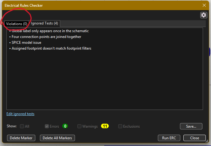
Figure: ERC completed successfully after resolving all warnings.
PCB Editor
Once the schematic design was completed and all component footprints were assigned, the design was transferred to the KiCad PCB Editor. The PCB Editor is used to create the physical layout of the circuit board by arranging components, defining board dimensions, routing electrical connections, and preparing the design for manufacturing.
The PCB Editor converts the logical schematic into a physical representation that can be fabricated. Components imported from the schematic appear outside the board area and must be positioned appropriately before routing begins.
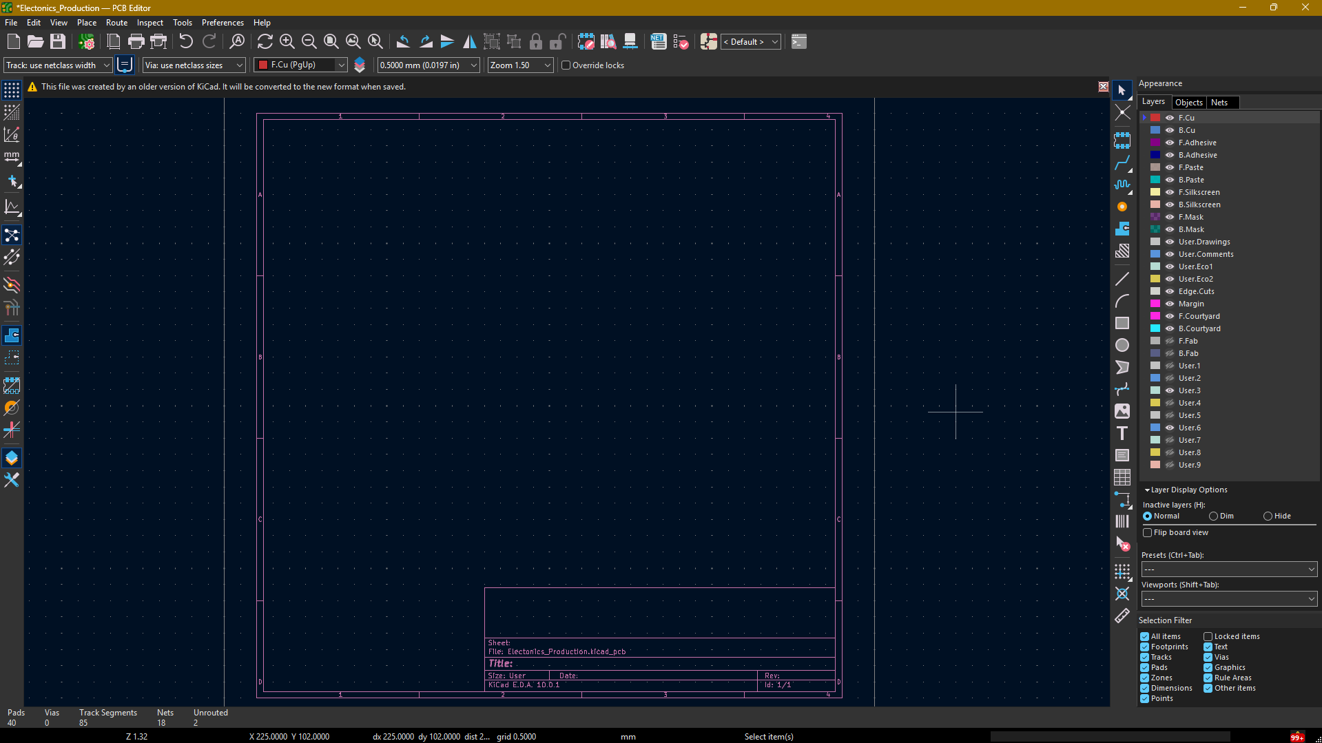
Figure: KiCad PCB Editor showing imported components ready for placement and routing.
Navigating the PCB Editor
Before beginning the PCB layout process, it was important to understand the tools available within the PCB Editor. KiCad provides several features that assist in board design, component placement, routing, verification, and visualization.
Main Areas of the PCB Editor
- Board Workspace: Main design area where components and tracks are placed.
- Right Toolbar: Contains tools for routing, vias, zones, dimensions, and graphical objects.
- Left Toolbar: Contains selection, placement, and editing tools.
- Layers Panel: Controls visibility of copper, silkscreen, edge cuts, and fabrication layers.
- Appearance Manager: Allows customization of colors and layer visibility.
- Properties Panel: Displays editable properties of selected objects.
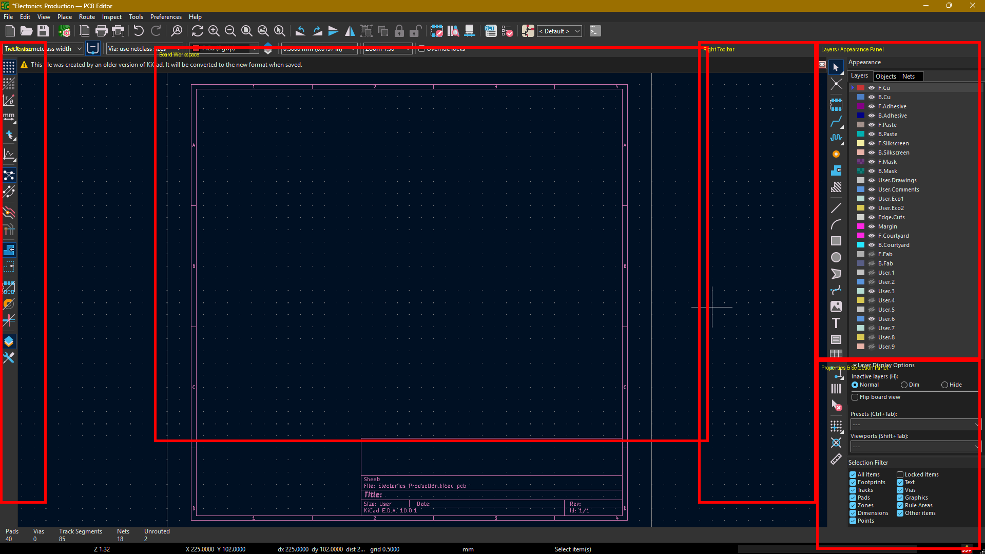
Figure: Overview of the major tools and navigation areas within the KiCad PCB Editor.
Understanding these tools improved workflow efficiency and simplified the process of placing components and routing electrical connections.
Updating PCB from Schematic
After completing the schematic design and verifying all electrical connections using the Electrical Rules Check (ERC), the next step was to transfer the schematic information into the PCB Editor. KiCad provides an Update PCB from Schematic tool that automatically imports the footprints and netlist information into the PCB workspace.
This feature ensures synchronization between the schematic and PCB layout. Any modifications made in the schematic can be reflected in the PCB design by running the update process again. During this step, all component footprints and electrical connections were transferred successfully into the PCB Editor.
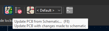
Figure: Updating the PCB layout from the completed schematic design.
Once the update process was completed, all footprints appeared inside the PCB workspace along with their corresponding ratsnest connections, which visually represent the electrical connections that must be routed on the PCB.
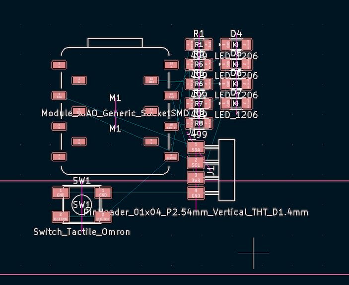
Figure 10: PCB editor showing component placement and routing workspace.
PCB Routing and Trace Creation
Once the component placement was finalized, the routing process was started. PCB routing involves creating copper traces that establish electrical connections between component pads according to the schematic netlist.
The Interactive Router tool in KiCad was used to route all required connections. The ratsnest lines provided a visual guide indicating which pads needed to be connected. Routing was performed carefully to avoid overlaps and maintain proper clearances between traces.
Since the board was designed for in-house PCB fabrication, routing was completed using a single copper layer. Appropriate trace widths were selected to ensure reliable manufacturing and electrical performance.
- Power connections were routed first.
- Signal traces were routed after completing the power network.
- Short and direct routing paths were preferred.
- Sharp corners were avoided to improve manufacturability.
- Proper spacing was maintained between adjacent traces.
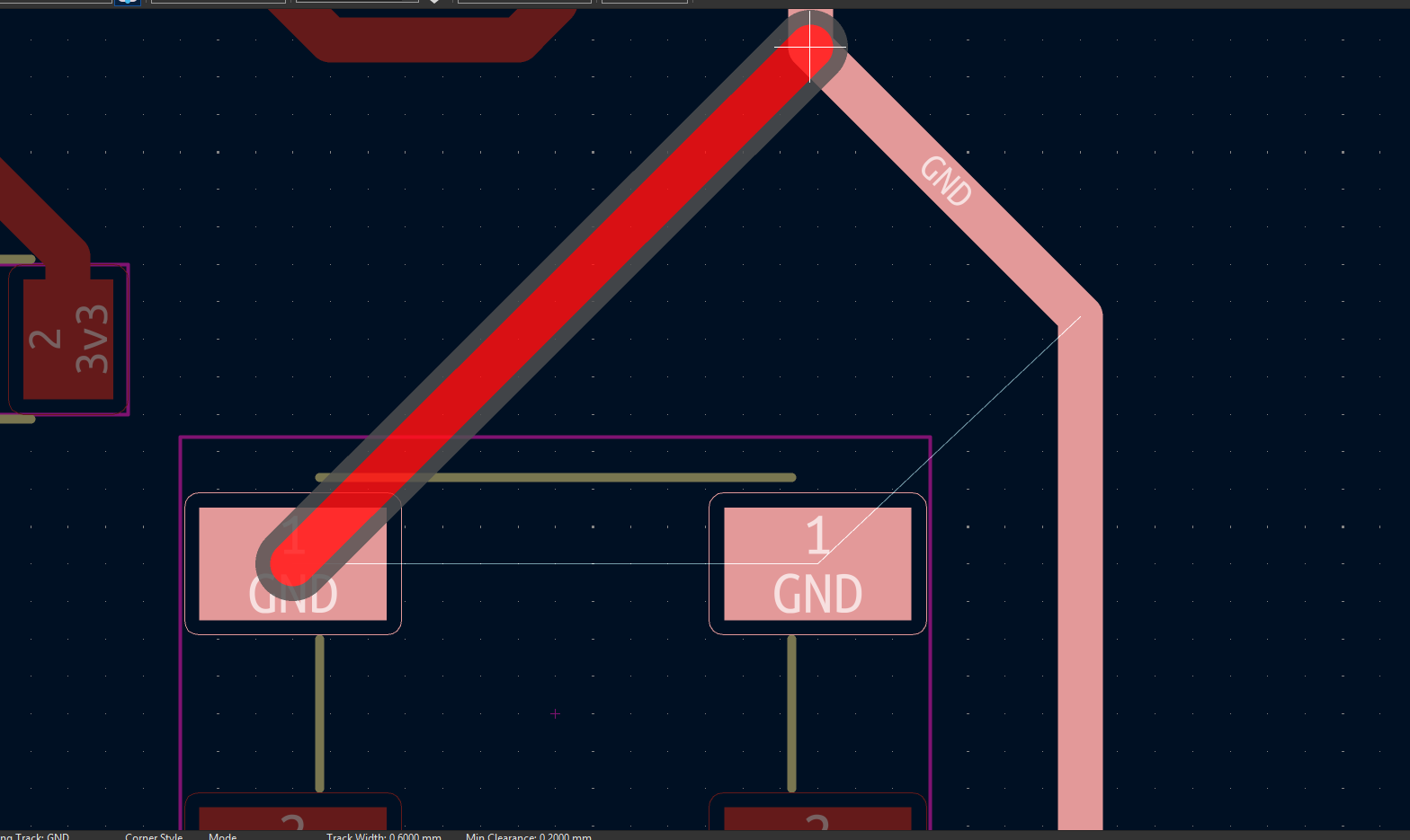
Figure: PCB routing completed using the KiCad interactive routing tool.
After routing was completed, all ratsnest connections disappeared, confirming that every electrical connection defined in the schematic had been successfully implemented on the PCB layout.
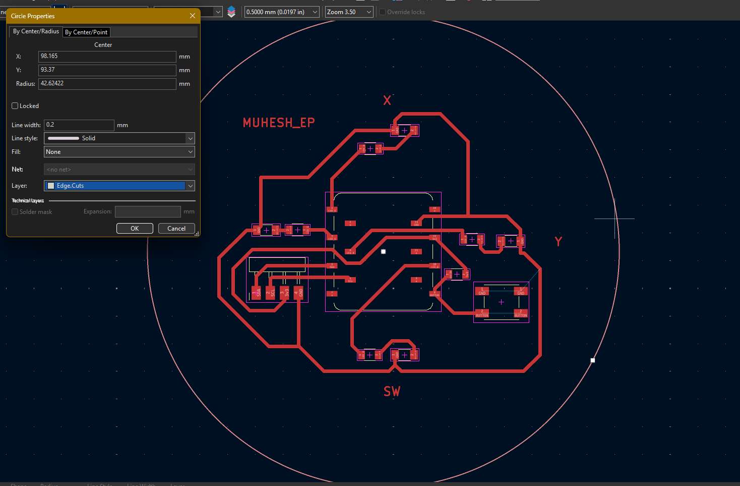
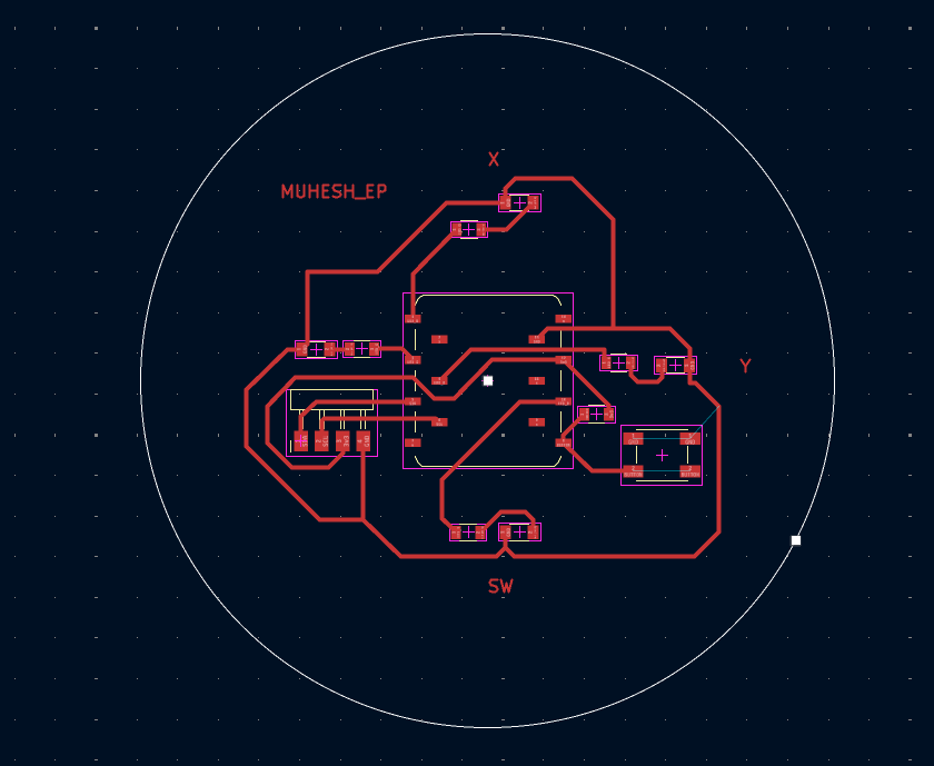
Board Outline Creation
The first step in PCB layout design was defining the physical dimensions of the board. Using the Edge.Cuts layer, a custom board outline was drawn to establish the final shape and size of the PCB.
The board dimensions were selected to accommodate the XIAO ESP32-C3 module, LEDs, push button, OLED connector, and programming interfaces while maintaining a compact form factor.
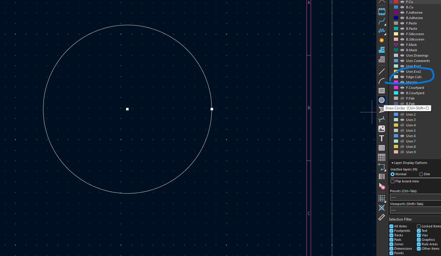
Figure: Board outline created using the Edge.Cuts layer.
Design Rule Check (DRC)
After completing component placement and PCB routing, a Design Rule Check (DRC) was performed to verify that the layout satisfied the manufacturing constraints of the PCB fabrication process.
The DRC tool checks for issues such as insufficient trace spacing, overlapping copper regions, unconnected nets, and violations of design constraints. Performing this validation helps ensure that the PCB can be manufactured successfully without electrical or mechanical issues.
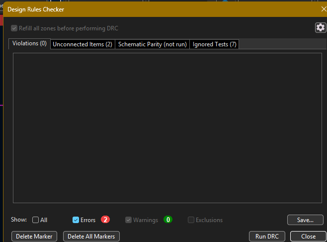
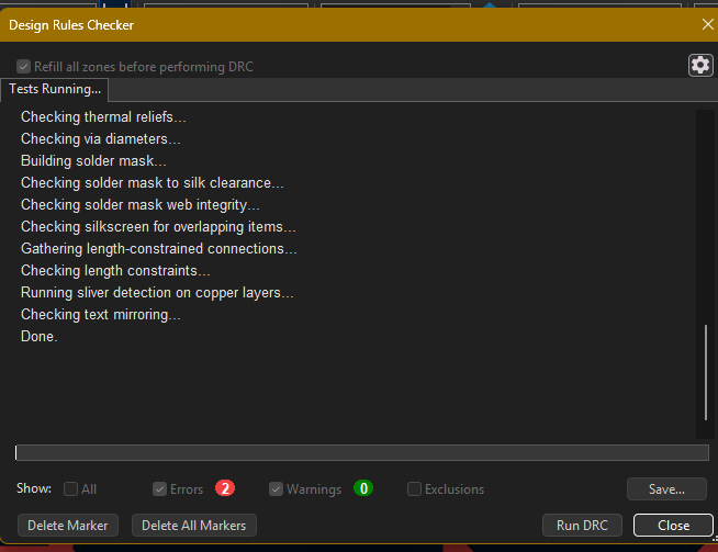
Figure: Design Rule Check performed on the completed PCB layout.
After correcting any reported violations, the PCB successfully passed DRC validation and was considered ready for fabrication.
Preparing for Fabrication
After successfully completing the DRC process, the PCB design was ready for fabrication. The next step involves generating manufacturing files such as Gerber files, drill files, and bill of materials, which are discussed in detail during the Electronics Production week.
View Electronics Production Documentation →
3D Viewer and Design Verification
After completing component placement, routing, and Design Rule Check (DRC) validation, the next step was to inspect the PCB using KiCad's built-in 3D Viewer. The 3D Viewer provides a realistic visualization of the printed circuit board and allows designers to verify the physical arrangement of components before manufacturing.
The 3D Viewer automatically generates a three-dimensional representation of the PCB using the assigned footprints and associated 3D models. This helps identify potential placement issues, orientation errors, mechanical conflicts, and overall board aesthetics.
Figure: Opening the 3D Viewer to inspect the completed PCB design.
Purpose of the 3D Viewer
- Visualize the PCB in a realistic three-dimensional environment.
- Verify component orientation and placement.
- Check connector accessibility and board usability.
- Identify possible mechanical interferences.
- Validate the final appearance before fabrication.
Using the 3D Viewer, the placement of the XIAO ESP32-C3 module, LEDs, push button, and OLED connector was inspected. The visualization confirmed that all components were correctly positioned and aligned according to the intended board design.
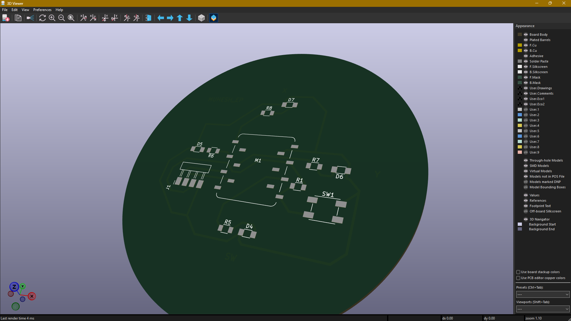
Figure: Final three-dimensional view of the completed PCB showing all mounted components.
The 3D inspection provided an additional layer of design verification before generating fabrication files. By reviewing the board in three dimensions, potential assembly and manufacturing issues could be identified and corrected before production.
Advantages of Using the 3D Viewer
- Improves confidence before fabrication.
- Provides realistic visualization of the final board.
- Helps detect placement and orientation errors.
- Supports mechanical integration planning.
- Reduces the risk of manufacturing mistakes.
Hero Shot
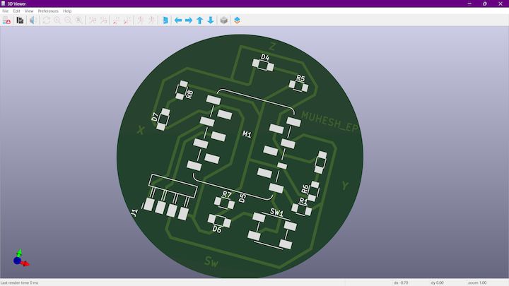
Figure 15: Final PCB design visualized using the KiCad 3D Viewer.
Learning Summary
- Learned the complete Electronic Design Automation (EDA) workflow and understood how electronic circuits are transformed from schematic diagrams into manufacturable printed circuit boards.
- Explored various EDA software tools such as KiCad, EasyEDA, Altium Designer, Eagle, and OrCAD, and understood their applications in electronic product development.
- Gained hands-on experience using KiCad for schematic capture, component selection, and circuit documentation.
- Learned how to select appropriate electronic symbols from the KiCad library and configure component properties according to design requirements.
- Understood the importance of schematic annotation and footprint assignment to ensure correct mapping between the logical circuit and the physical PCB layout.
- Performed Electrical Rule Check (ERC) to identify connectivity issues, missing pins, and potential schematic design errors before proceeding to PCB layout.
- Learned how to transfer a completed schematic into the PCB editor and organize components for efficient routing.
- Developed an understanding of PCB design principles including component placement, trace routing, clearance requirements, and board organization.
- Implemented a ground plane and understood its role in reducing noise, improving signal return paths, and enhancing overall circuit reliability.
- Performed Design Rule Check (DRC) to validate the PCB layout and ensure that the design met manufacturing constraints.
- Learned how to use the KiCad 3D Viewer to visualize the final PCB before fabrication and verify the placement of components.
- Gained a clear understanding of the preparation steps required before PCB fabrication, including verification, design validation, and generation of manufacturing files.
Finally Leaving my files here
Contents
- Objectives of the Week
- Group Assignment Contribution
- EDA Tools
- Why KiCad?
- Learning Resources
- KiCad Workflow
- Creating a New Project
- Schematic Editor
- FabLab Repo Libraries
- Importing Symbols
- Global Labels
- Assigning Footprints
- Annotating the Schematic
- Initial ERC Check
- Adding Power Flags
- Final ERC Verification
- PCB Editor Navigation
- Updating PCB from Schematic
- Component Placement
- PCB Routing and Trace Creation
- Design Rule Check (DRC)
- 3D Viewer and Design Verification
- Generating Fabrication Files
- PCB Production
- Learning Summary
- Hero Shot
- Design Files