#8 Electronics Production
This week I learned how to fabricate PCB.
Assignment
Group assignment
- Characterize the design rules for your in-house PCB production process: document feeds, speeds, plunge rate, depth of cut (traces and outline) and tooling
- Document the workflow for sending a PCB to a boardhouse
Individual assignment
Outcomes
What did I do this week: 1. Group Assignment
The group assignment page - week08
Characterize the design rules for your in-house PCB production process: document feeds, speeds, plunge rate, depth of cut (traces and outline) and tooling
This week, we tested design rules for Roland-SRM20 with test-cut data.
we tried 3 different mills.
Here are some notes for meaning of each parameter in mods tool settings:
tool diameter (in) : Diameter of the blade
cut depth (in) : How much to cut in one pass (if it is too high, the load on the blade is high)
max depth (in) : Roughly the same value
offset number : If it is 0, it is fill
offset stepover : Interval for offset
speed (mm/s) : Speed
Document the workflow for sending a PCB to a boardhouse
For details, please see the group page: The group assignment page - week06
What did I do this week: 2. Individual assignment
Make and test a microcontroller development board that you designed
Procedure
In the class, several methods of PCB(Printed Circuit Board) fabrication (etching, machining,
cutting, etc.) were introduced.
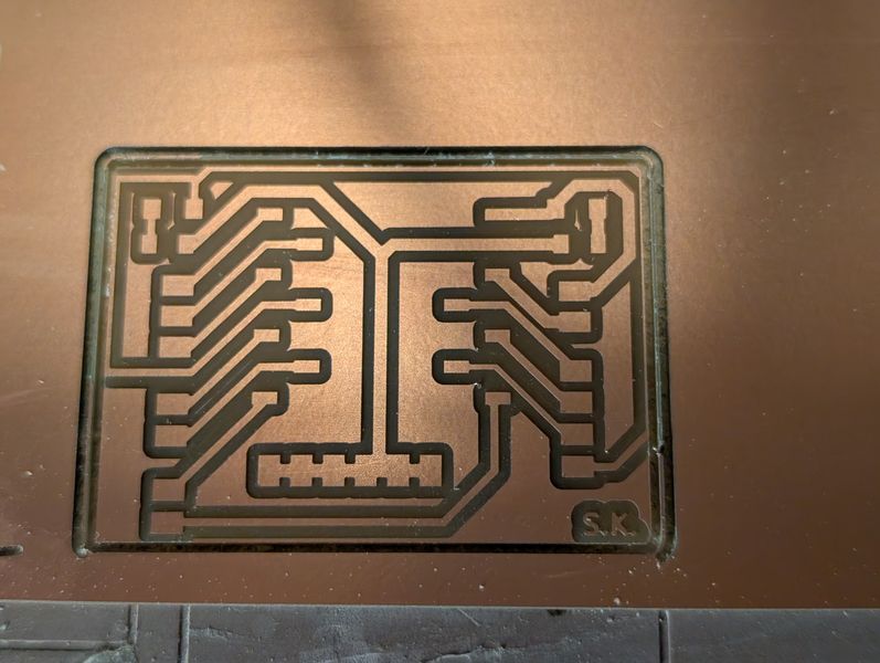
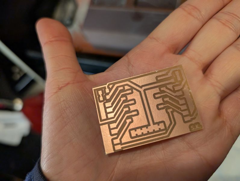
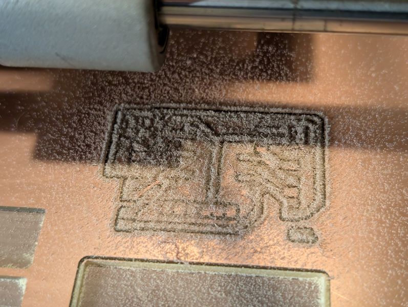
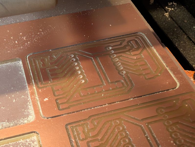
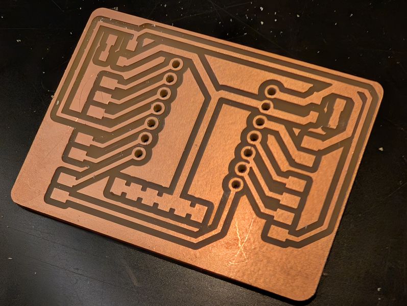
This time, I tried Machining as per usual. In FabLab Kamakura, we used Roland-SRM20.
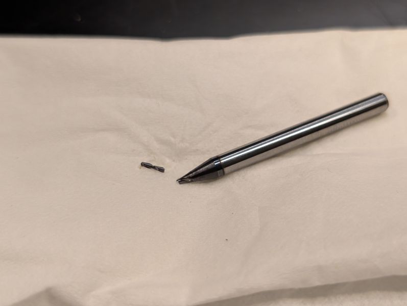
As for tooling, I used 1/64 for tracing and 1/32 for cutting and holes.
As for PCB material, I used FR1 (phenolic paper).
As for CAM, I used “mods”
And finally, solder them.
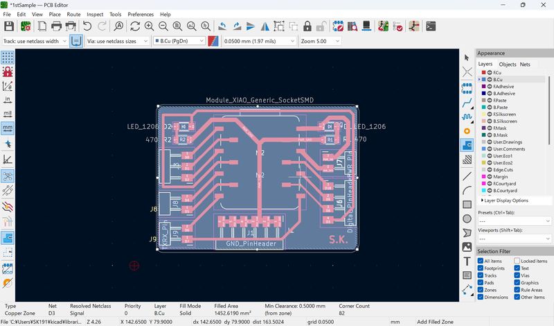
0. PCB design modifications
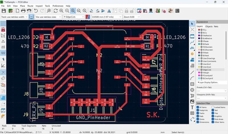
I changed track width as 0.6mm, since I am a bigger and it might be difficult to solder.
I ran the DRC(Design Rule Checker) and it gave me errors because some of the circuits
lines
were too close together, so I fixed the design.
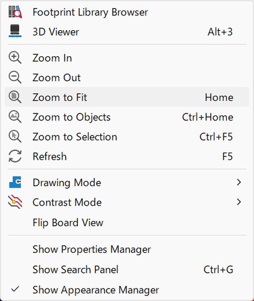
If you lost the view, you can come back
with ‘Zoom to Fit’
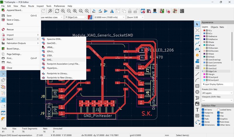
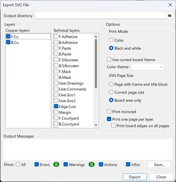
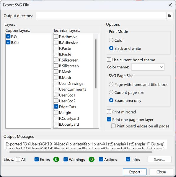
1. Export as svg file
Before exporting, there are a few things you need to check.
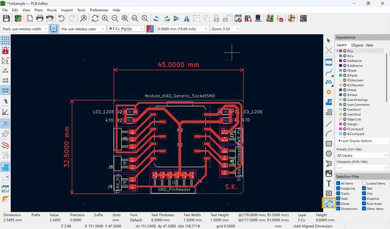
1.Measure the size.
Go to “Add Aligned Dimension” tool and measure the dimension
2.Add Fit Zone (Important!!!)
Select the Add Fit Zone menu and surround the area of the circuit.
Then go to Zones > Select Fill All Zones.
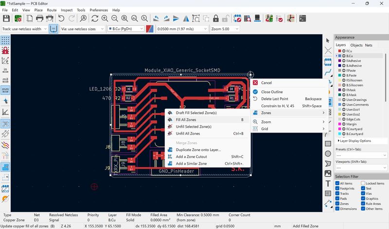
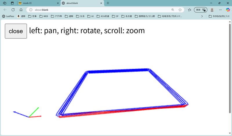
*At first, I cut without this setting, and a strange line was made on the inside, and when that line was cut, the circuit line was broken. (See image below) It took me a long time to figure out this setting.
3.Export as svg
Go Export > SVG
Choose F.cu layer and B.cu Layer, and
Edge. cuts layer.
Print mode: black and white
Page size: Board area only
Check Print one page per layer
Then, press “Export”
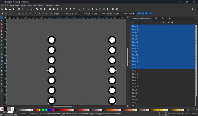
When making holes, edit the data for the hole and the circumference separately using a vector tool such as Inkscape. When doing so, be careful not to move the location of the data. (To prevent misalignment when cutting.) *Leave inside hole and make them black. Delete hole outer line with black
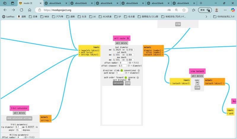
CAM - mods
The basic usage is explained here(Japanese) : https://fablabkamakura.fabcloud.io/FabAcademy/local-sessions/week8/
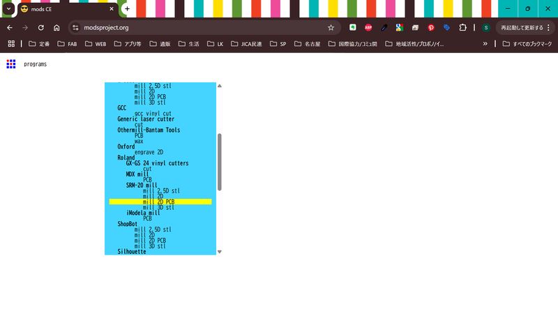
Open mods
Right click > Program > Open Program > Select Roland SRM20 mill 2D PCB
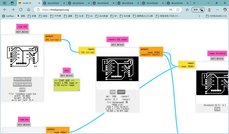
Open svg file from “read svg” section
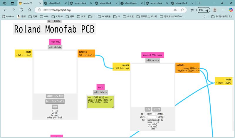
Check if the size is correct compared to what I measured on the PCB design earlier.
To trace line, press “invert” in “convert SVG image” section
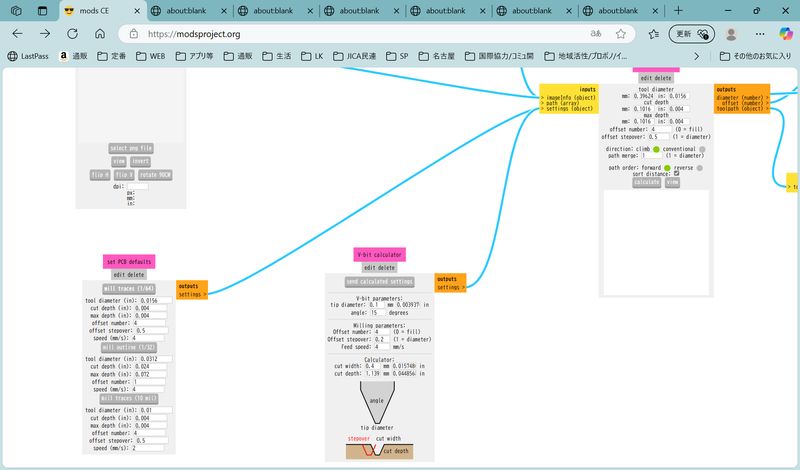
Set tool.
To trace, choose “mill traces(1/64)” in “set PCB defaults” section and 1/64 tool path
parameters will be reflected in the mill raster 2D section.
*For peripheral cut or hole drilling, choose "mill trace 1/32" in "set PCB
default" and 1/32 tool path parameters will be reflected in the mill raster 2D section
Set origin as 0 in “Roland SRM-2D milling machine” section
*The default is 10, and if you cut it like this it will cut through the air.
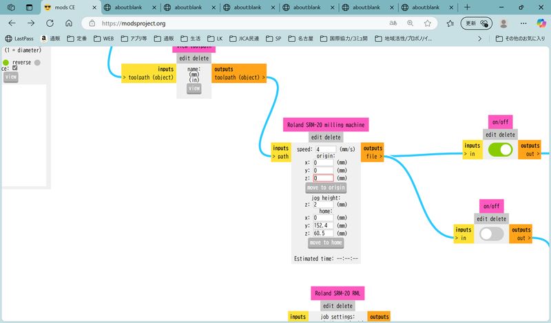
Set On for save file
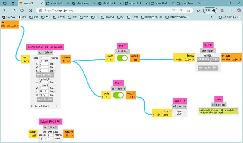
Press calculate.
The pass data will be generated and the file saved for your machine automatically.
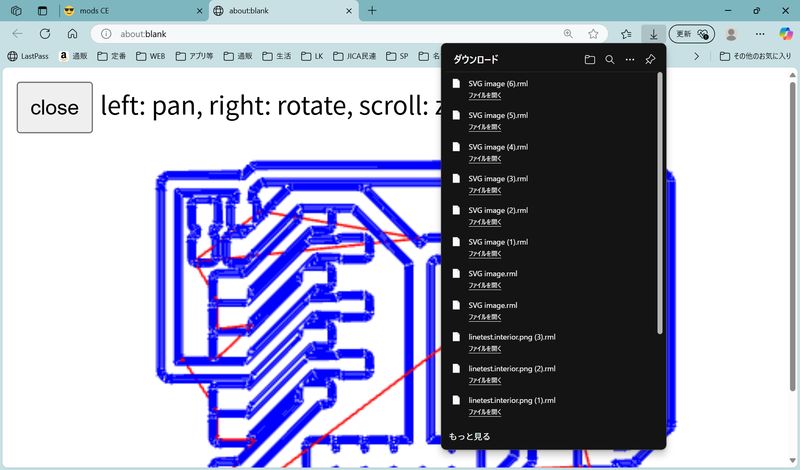
Be sure to close the image using the close button. To set for hole/outline, change tool setting and calculate it.
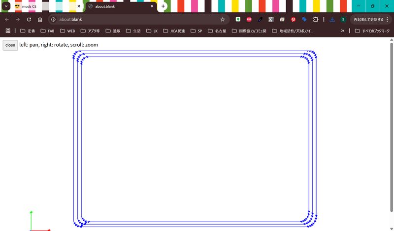
*Be careful: if you don't “add fit zone” in PCB editor , you'll get a strange path like this:
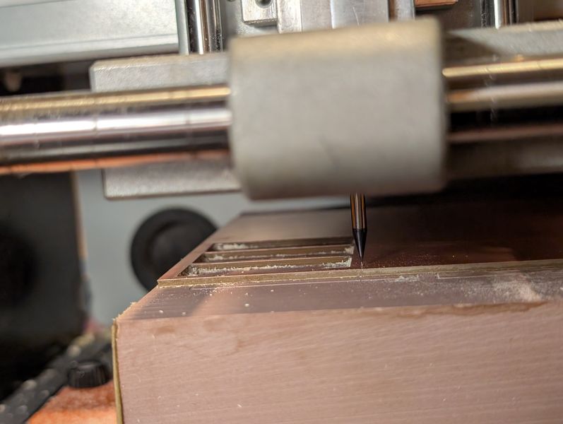
Machining
We used Roland-SRM20.
1.Set the endmill.
First, start from tracing. So I set the 1/64 mill.
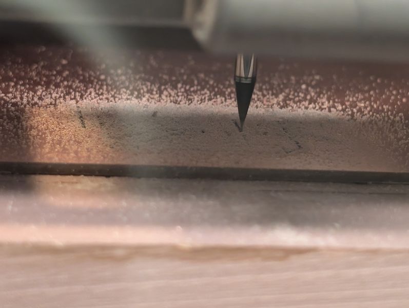
2. set x/y origin (work home)
Set the part you want to cut as 0, not the origin on the machine
Be sure to press X/Y on “Set Origin Point” section and confirm if it turns 0!3. set z origin
(work home)
When you bring the tip of the end mill as close as possible to the board using the button on
the screen, gently drop it onto the board and close the collet. Pressing it slightly onto the
board will allow for better cutting.
Be sure to press Z on “Set Origin Point” section and confirm if it turns 0!
(Important!!!)Points to note:
- If the mill is not firmly attached to the board, it will not be able to cut and will end up cutting through the air.
- If you forget to press the z0 set button and z0 is not set, the mill will go too far down and break.
- Once set, raise the Z axis!
4.Press cut button and select the file you want to cut.
Before selecting a file, delete all other files that are selected.
Press “Output” to start milling.
To cut outline, we have to change mill and z0.
Be careful not to change the x/y0 settings!!
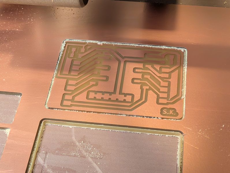
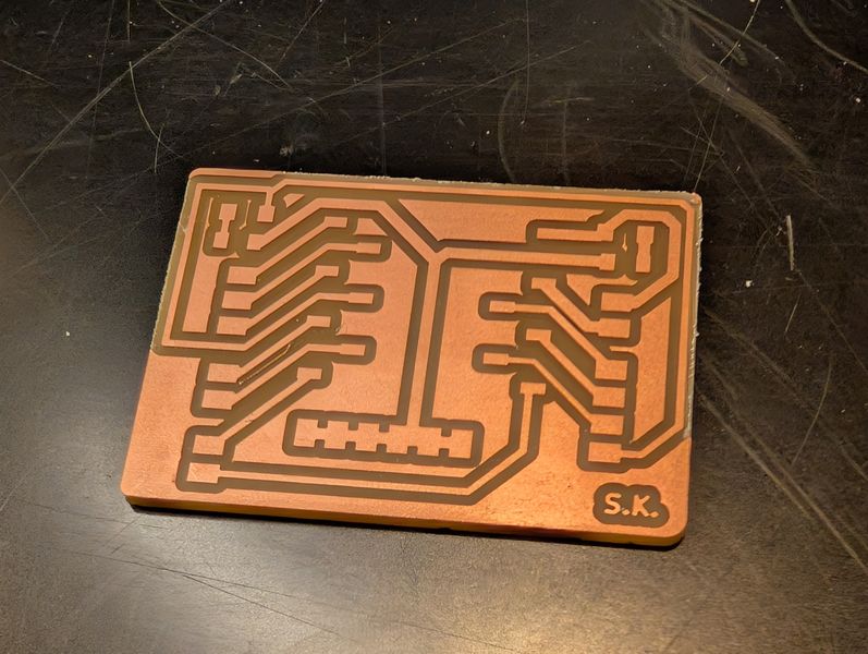
I also tried the design with hole: 1 trace (1/64 mill) > change mill and z0 to 1/32 mill > 2 hole > 3 outline
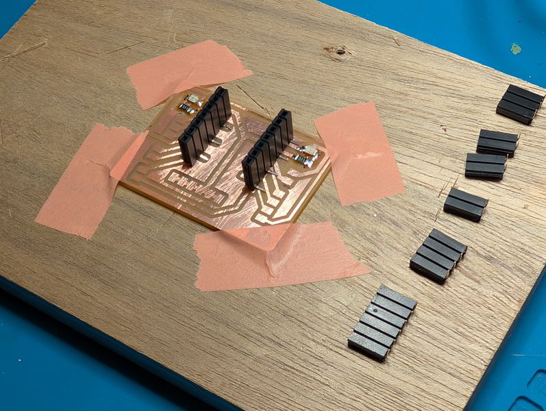
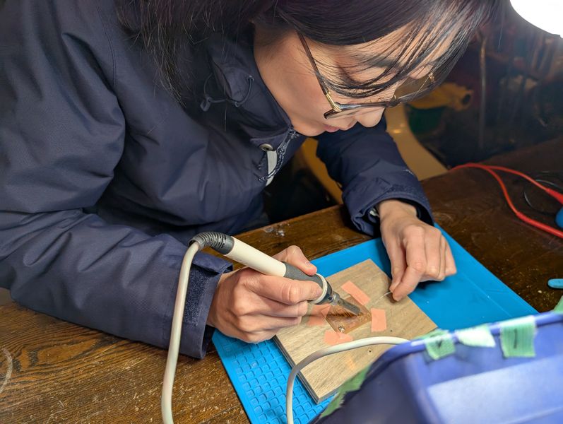
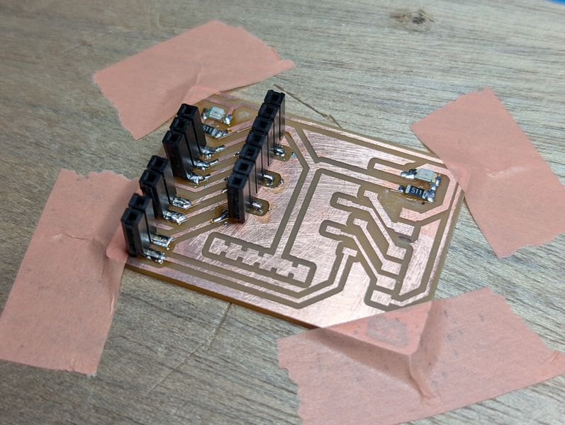
Soldering
1. Preparing - Circuit Board
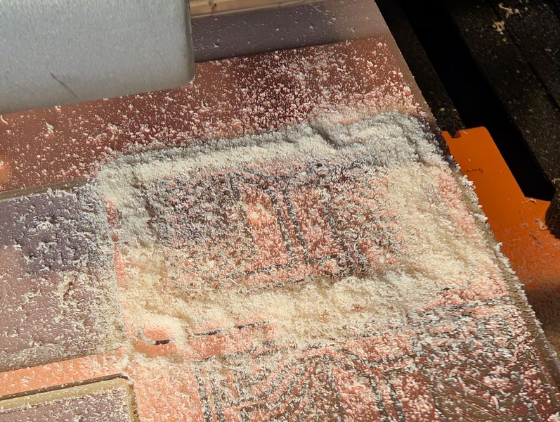
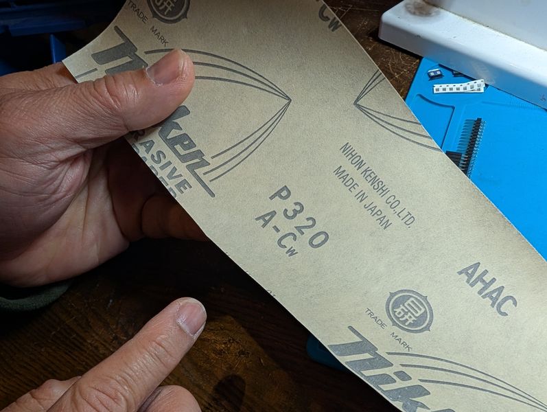
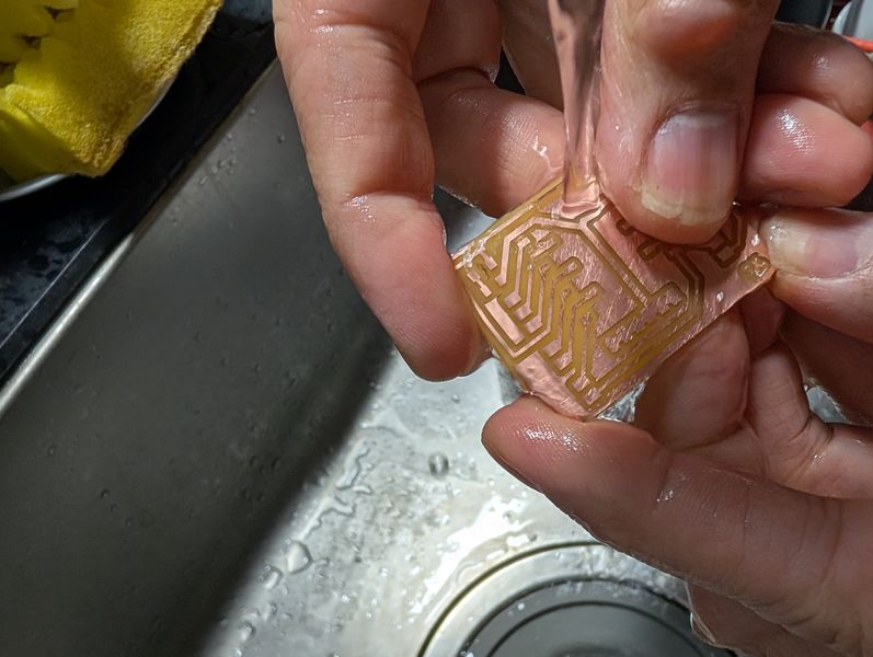
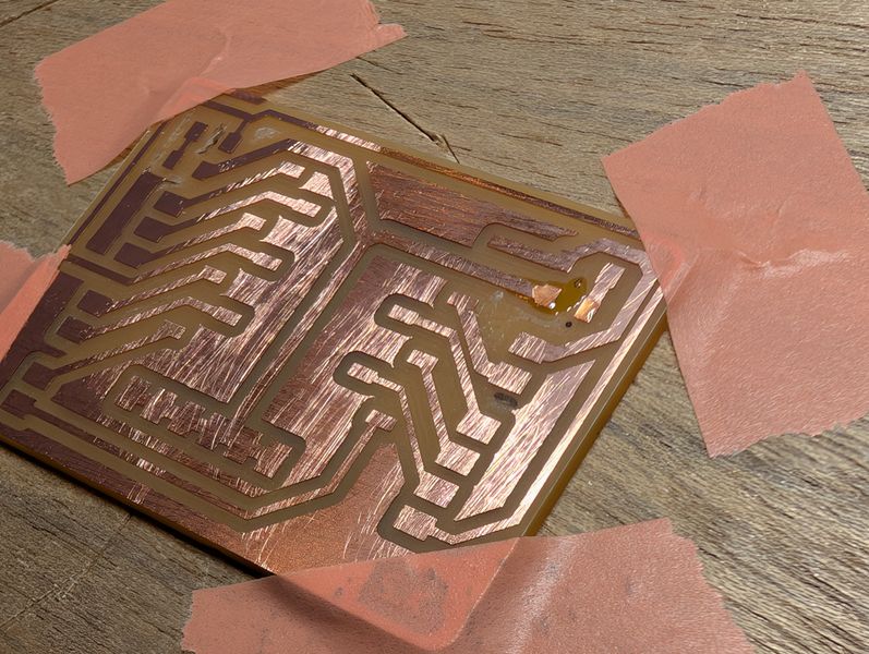
Once the board is cut, sand down with steel wool or very fine sandpaper
to remove any excess copper.
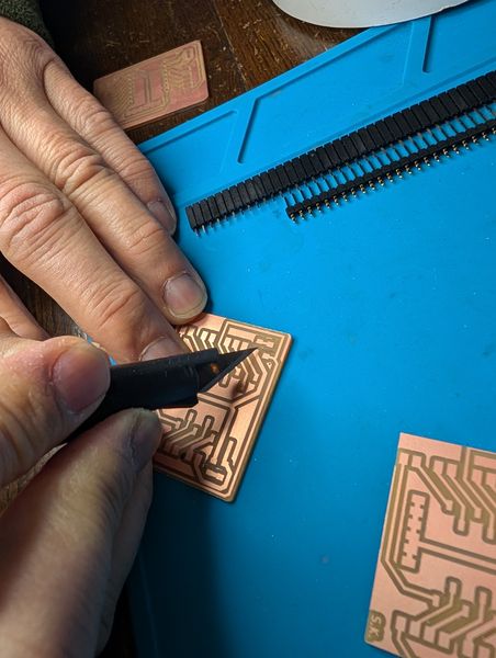
If there is any copper remaining that could get in the way and accidentally connect the
circuit when soldering, use a cutter or ultrasonic cutter to remove it beforehand.
(Carve up, not dig it)
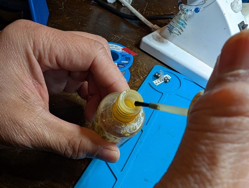
Also, wash it thoroughly with detergent to prevent oils from your hands from interfering
with the soldering process.
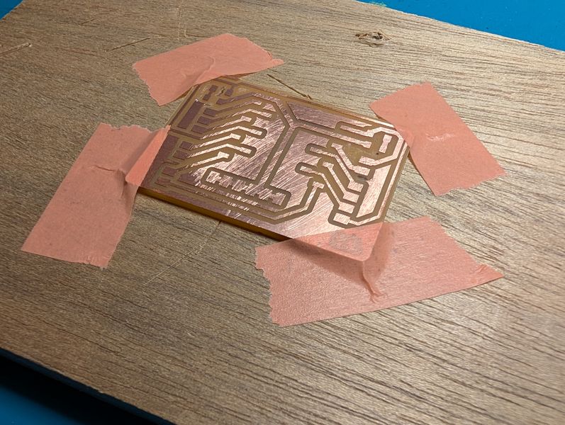
Then, fix it on a wooden board or other surface so that it cannot be touched by hands.
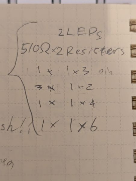
2. Preparing - List up the components
Make a list of the components you need and prepare what you need.
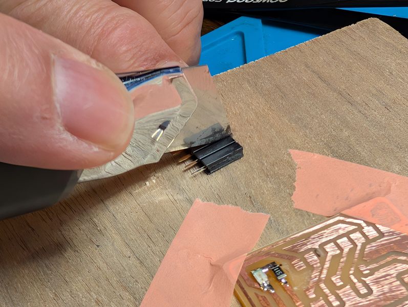
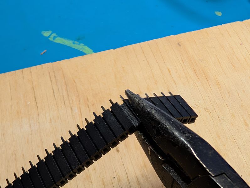
The original design using a male pin, but I changed it to a socket (Rico-san's
suggestion).
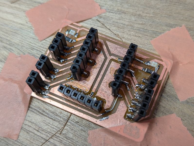
3. Soldering
The soldering order is as follows:
- lowest parts to highest parts
- inside to outside
- cleaning
- smoothing
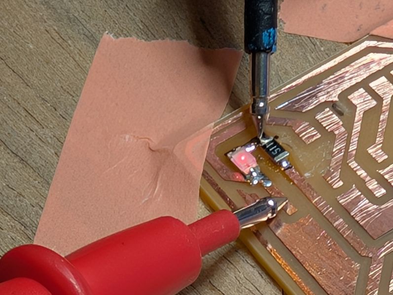
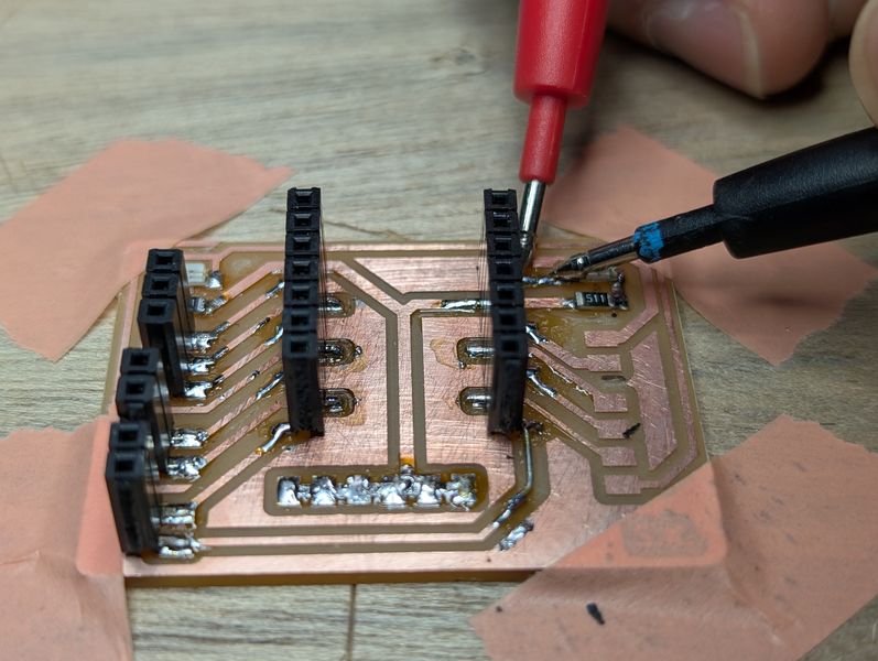
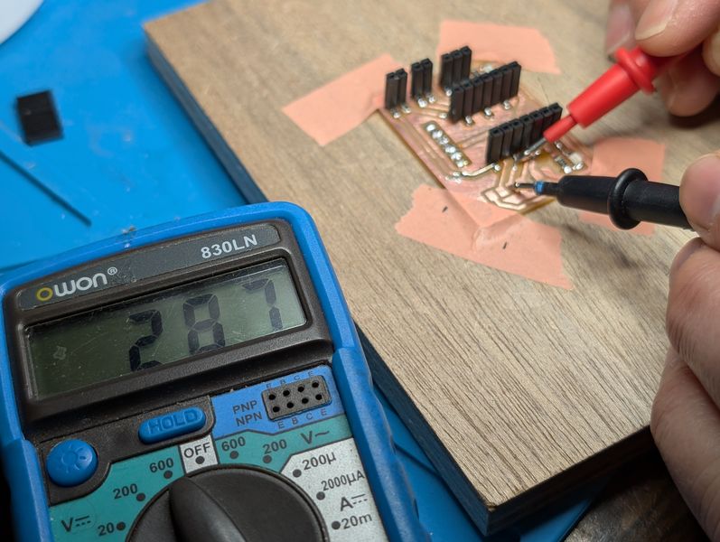
For items that have polarity, such as LEDs, check the direction with a multimeter before put them.
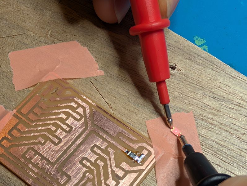
Once the parts are installed, use a multimeter to check that they are powered.
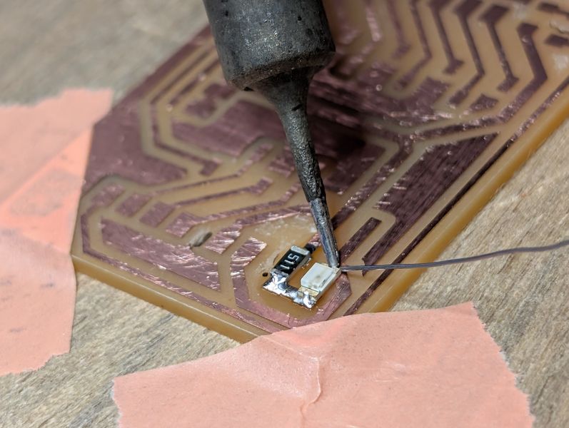
It was difficult since the parts were close to each other, but I was able to get them to stick more firmly by using plenty of flux and solder. While we were checking the socket distance to see if it fits the xiao, something happened. The copper wire came off. We used a wire to fix it.
Test
Once the circuit board was complete, I tested it with the sample code to see if it worked.
The code I used is below.
  #define led_pin D3

  void setup() {
    Serial.begin(115200);
    pinMode(led_pin, OUTPUT);
  }

  void loop() {
    Serial.println("Red");
    digitalWrite(led_pin, HIGH);
    delay(500);
    digitalWrite(led_pin, LOW);
    delay(500);
  }
It worked fine on the first test.
Outcomes
I could learn whole process of PCB fabrication by myself!
Some steps have the potential to damage the equipment, so I need to proceed with care.