Assignment
Individual Assignment:
- Make and test the development board that you designed to interact and communicate with an embedded microcontroller
- Extra credit: Make it with another process
Group Assignment
Our group assignment this week was to characteriz the design rules for our in-house PCB production process. We would receive extra credit if we sent our PCB out to a board house.
The link to our group work page can be found here.
Our Test Results
We have two options for PCB milling in house
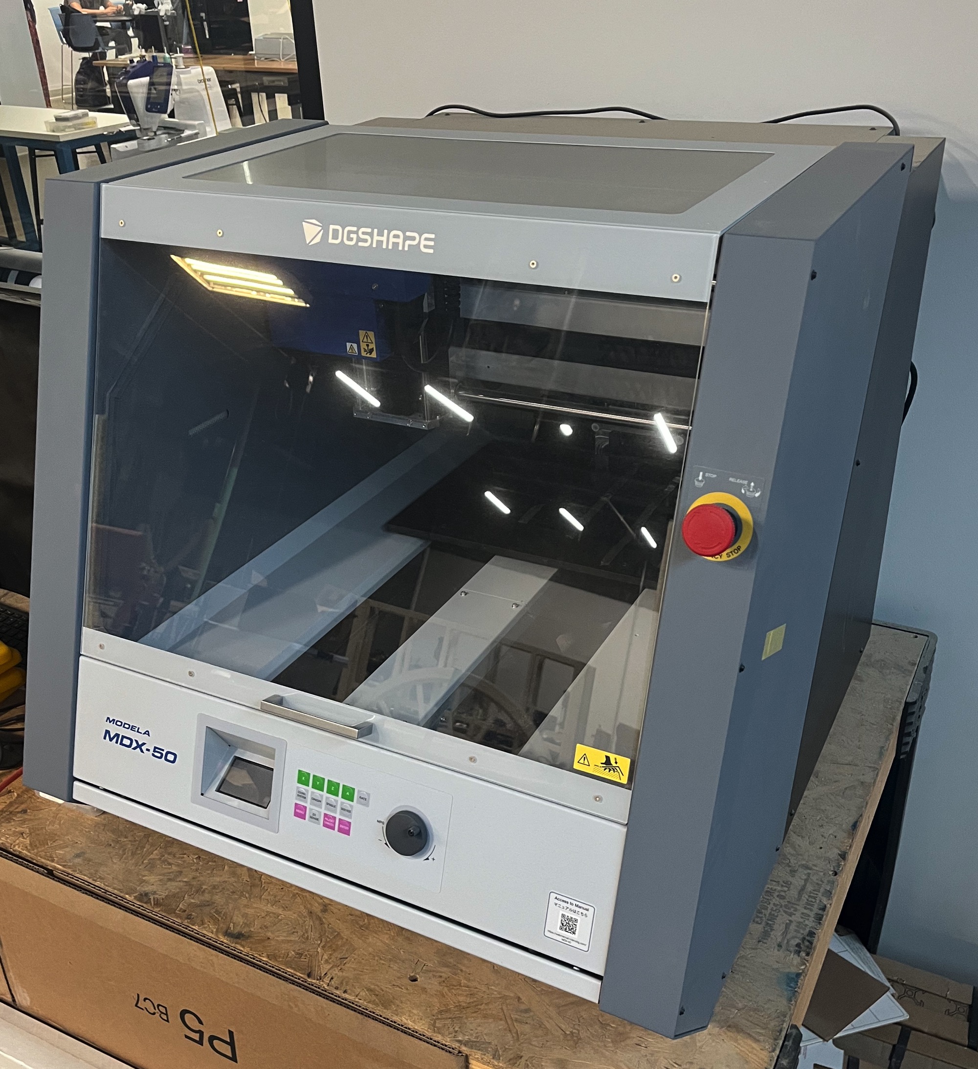
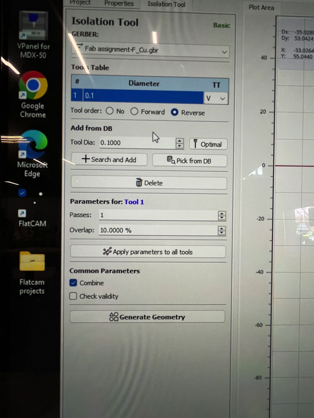
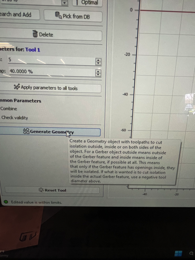
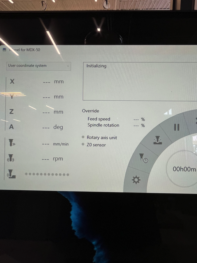
Characterizing the Modela MDX 50.
- Model: Roland Modela MDX-50
- Software: Roland's SRP Player for generating tool paths and contolling the milling process.
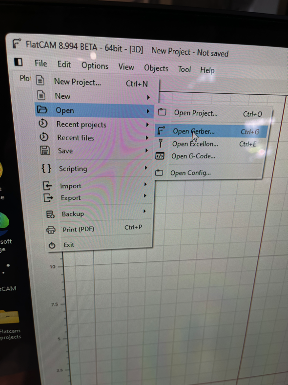
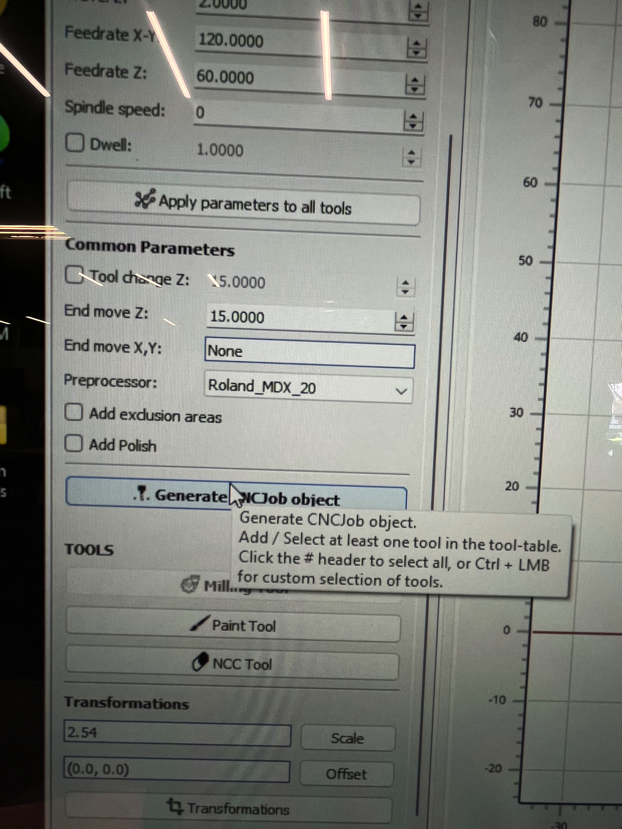
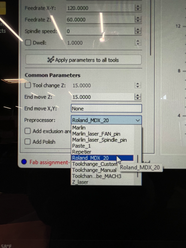
- Process: After the KiCad files are created we export the plot as a Gerber file that can be opened in FlatCam to create the tool paths for milling.
- Settings: Setting for MDX are found in images below in the Individual assignment section.
- Specifications: Output from FlatCam is imported into the SRP Player.
- Tools: 1/64 end mill
- Material: FR-1 PCB Board
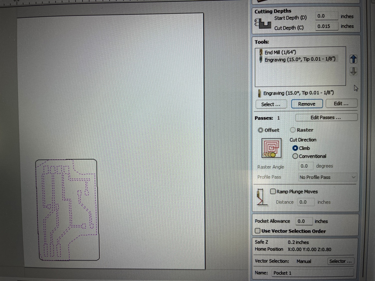
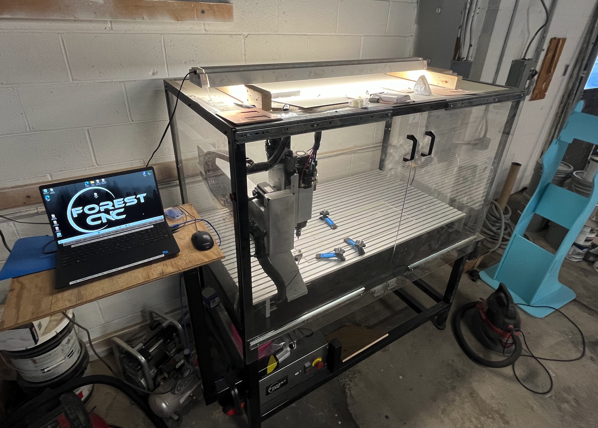
Characterizing the Forest ATC CNC,
- Model:ForestCNC ATC CNC
- Software: Vectric Cut2D Pro
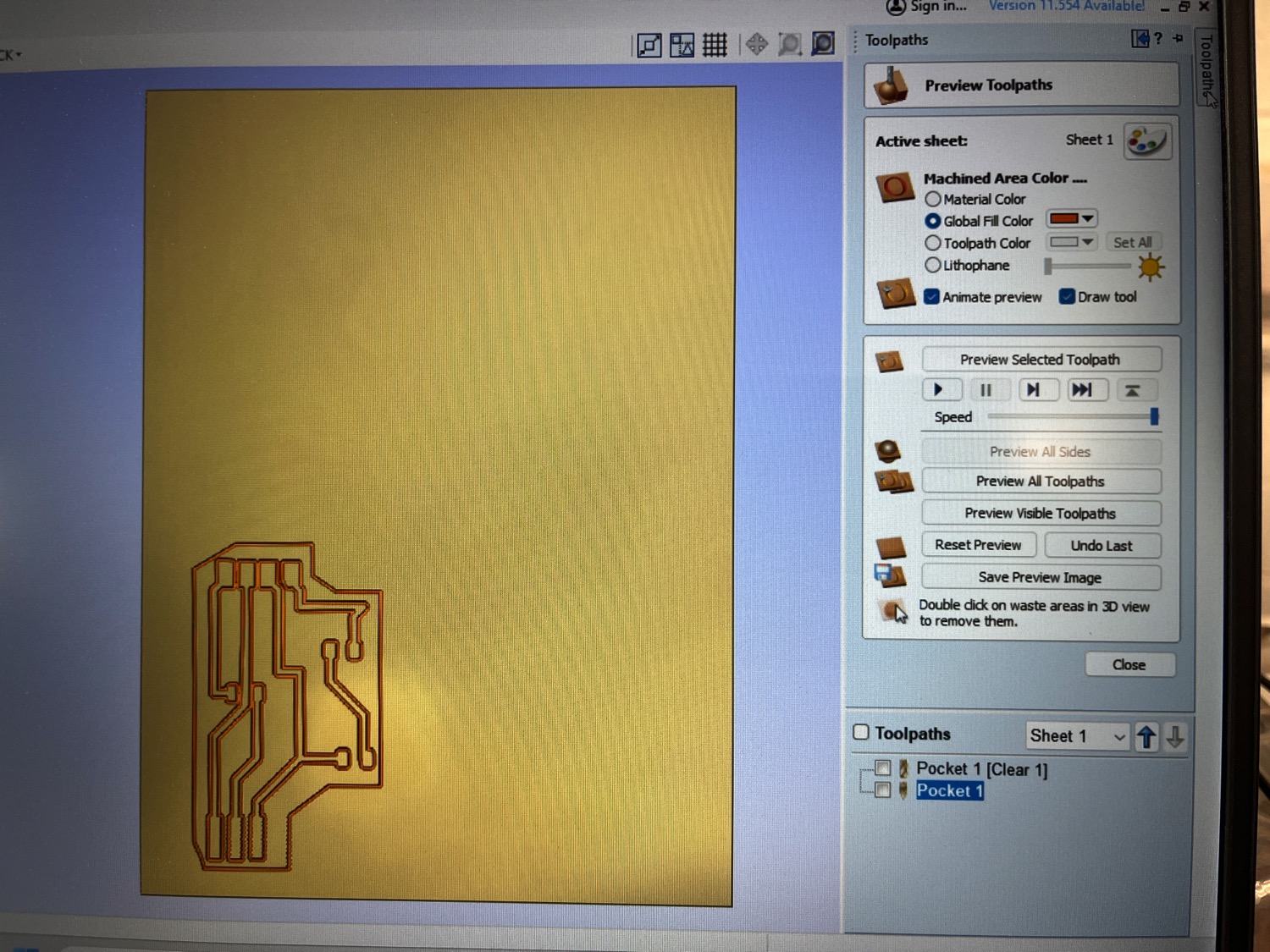
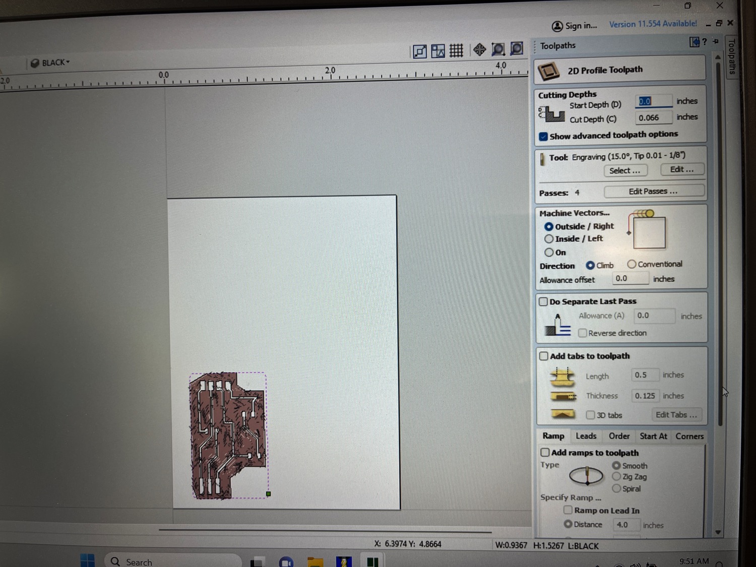
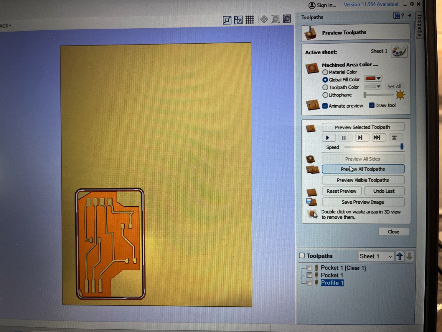
- The Process: This is different that when using the MDX. First we export the plot from KiCAD as a DXF file that can be opened in Cut2d Pro and will maintain proper dimensions. Once in Cut2D Pro we create a "pocket" tool path for the traces and then a profile cut for the edge cuts. The images below show the settings for the pocket and profile cuts.
- Settings:
- Tools: 1/64 end mill, 10 degree engraving bit, 15 degree engraving bit
- Material: FR-1 PCB Board
In House Electronics Production at PAST
Our task is to characterize our in-house design rules for PCB production
PROCESS
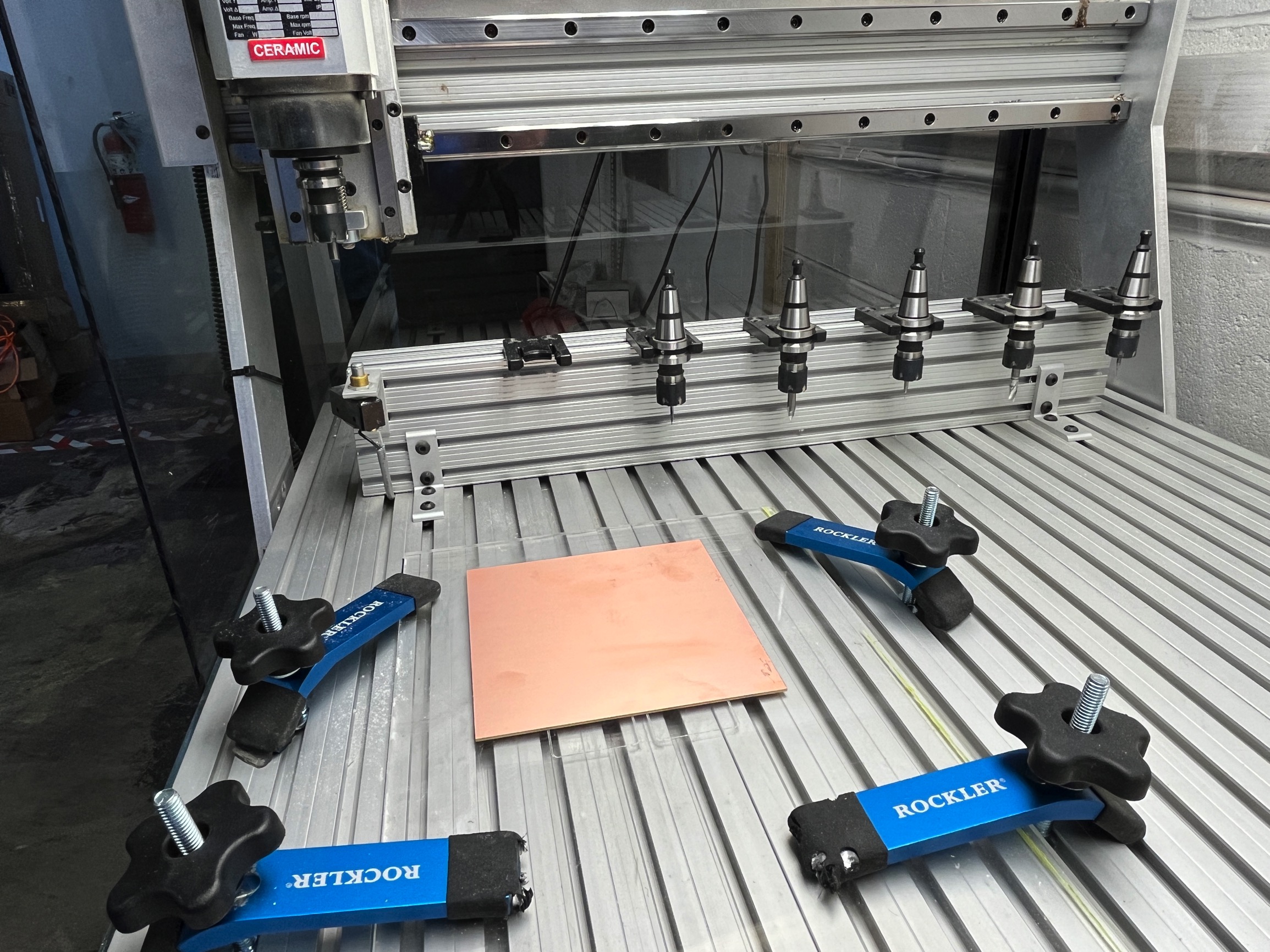
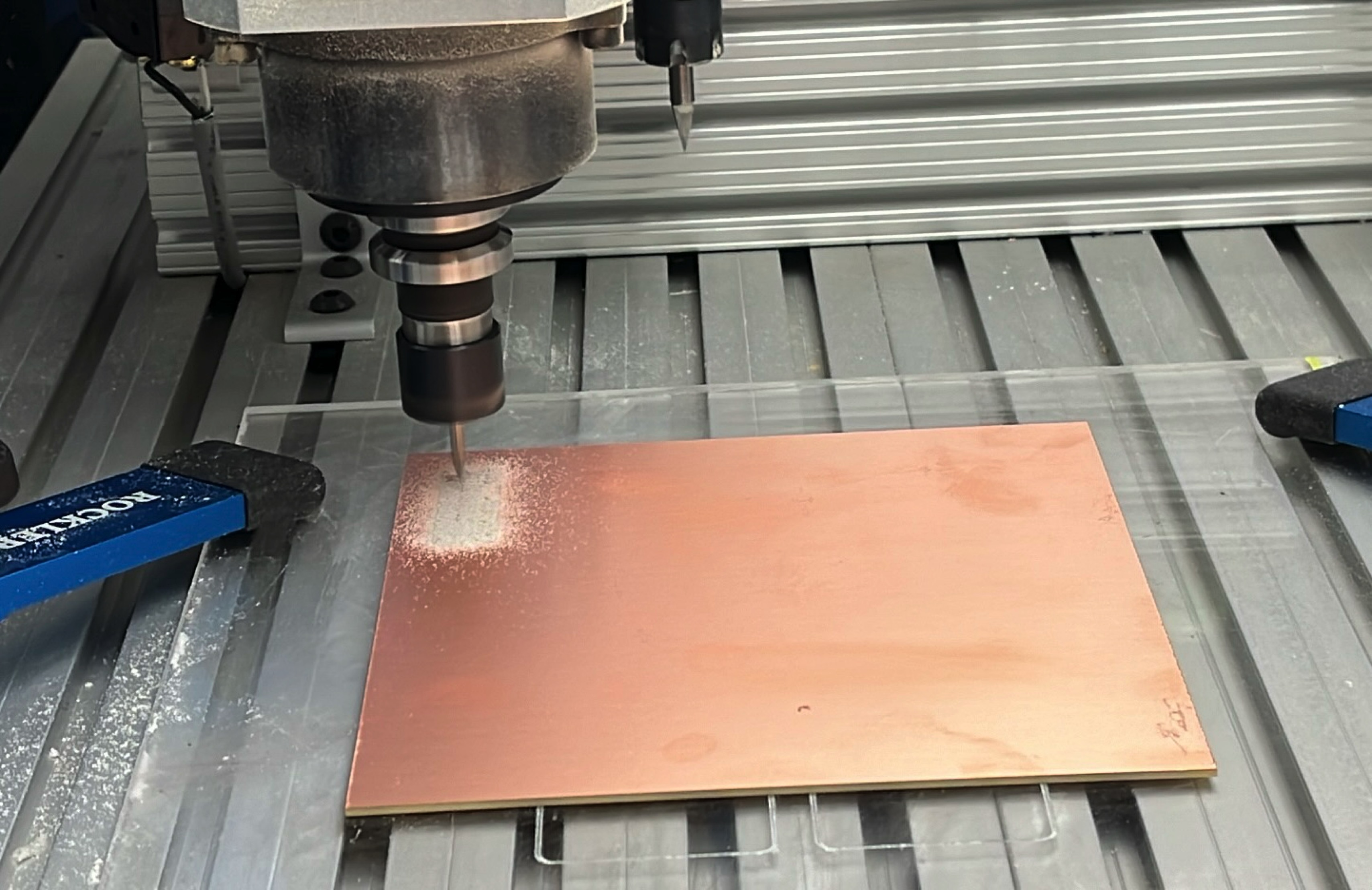
- First we have to secure the PCB blank to the milling machine cutting area. We use double sided tape to stick the blank to the cutting surface. Make sure the surface (polycarbonate sacrificial board) is clean and smooth.
- Using the Forest Scientific CNC interface manually set X, Y and Z for the material.
- Next, load the saved file from Cut2D Pro so begin milling.
- If board is un-level your milled PCB will not turn out properly.
- Adjust Z height and test again to be sure you have proper level of board.
- Finally, remove PCB after final edge cut is complete.
We will be using our milling machine to remove copper from the PCB board to create circuit traces.
We still have some tweaking to do to make sure the pcb blank is nice and level but ultimately we can create pcb boards with the process listed above.
Individual Assignment
- For the assignment this week, I started with the example circuit we made a few weeks ago. It took some time to research how to use the Modela MDX 50. Of all the machines in our lab the MDX 50 is one of the newest and as a result we are not as familiar with it.
- Honestly, I was hoping that my familiarity with the other CNC machines in our lab that that all I would need to do was to find the application that would convert the KiCad traces to CNC tool paths but it turned out to be more difficult that I thought.
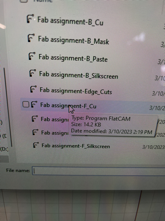
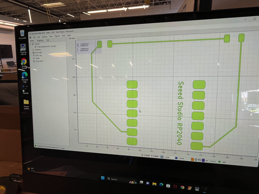
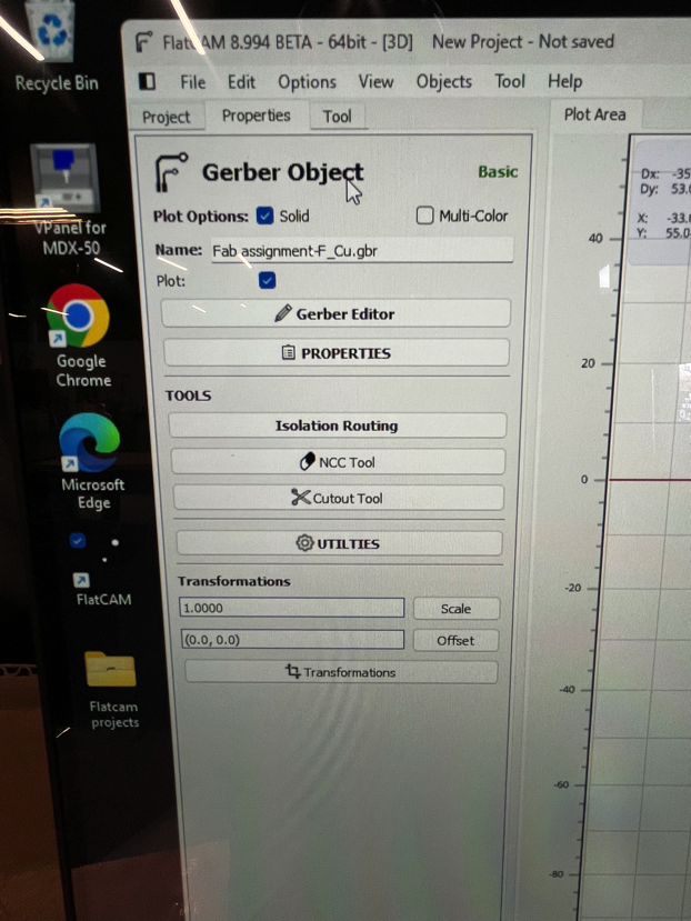
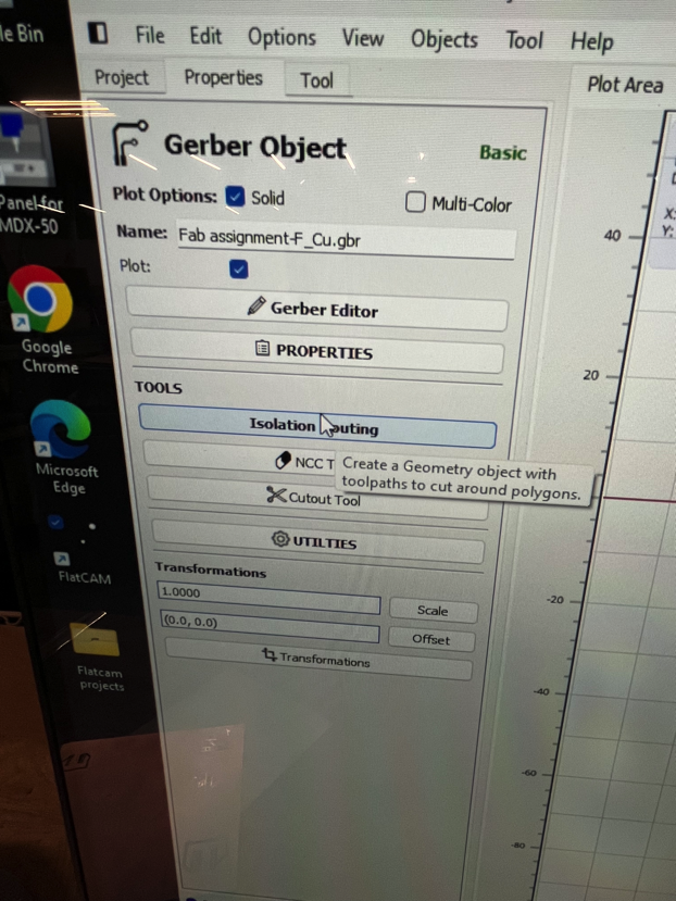
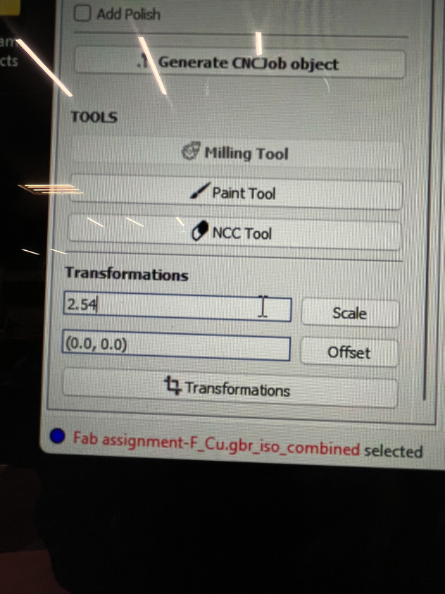
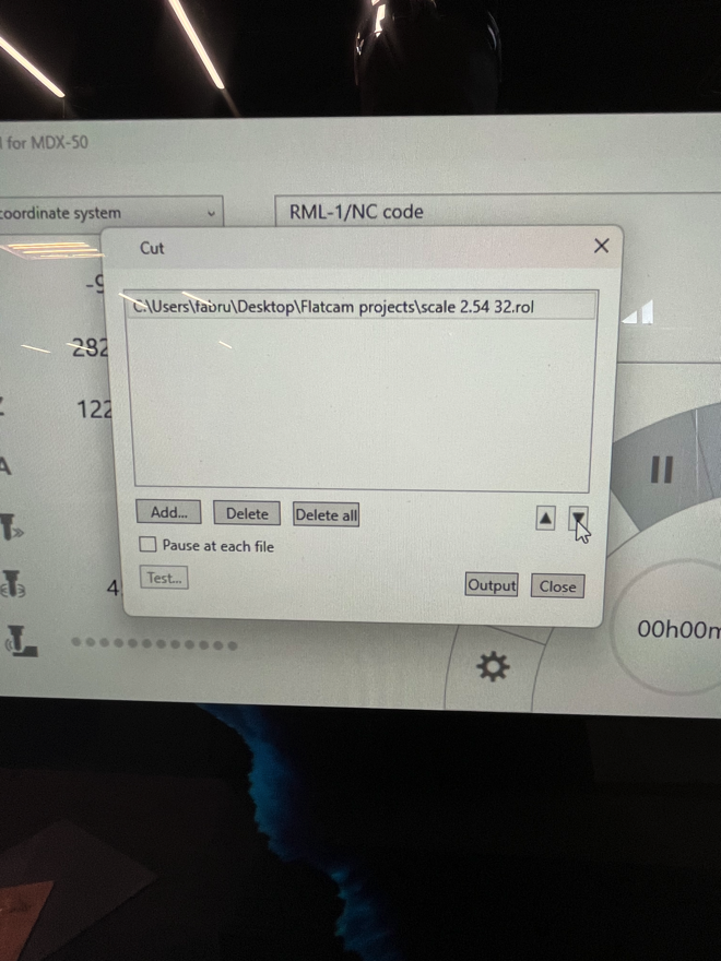
- I found flatcam and PCB2gcode for MacOS but for some reason I was not able to properly install them. I ultlmately, installed Flatcam on the Windows computer conncected to our MDX 50 and was able to create the tool paths and eventually send the file to the MDX for milling.
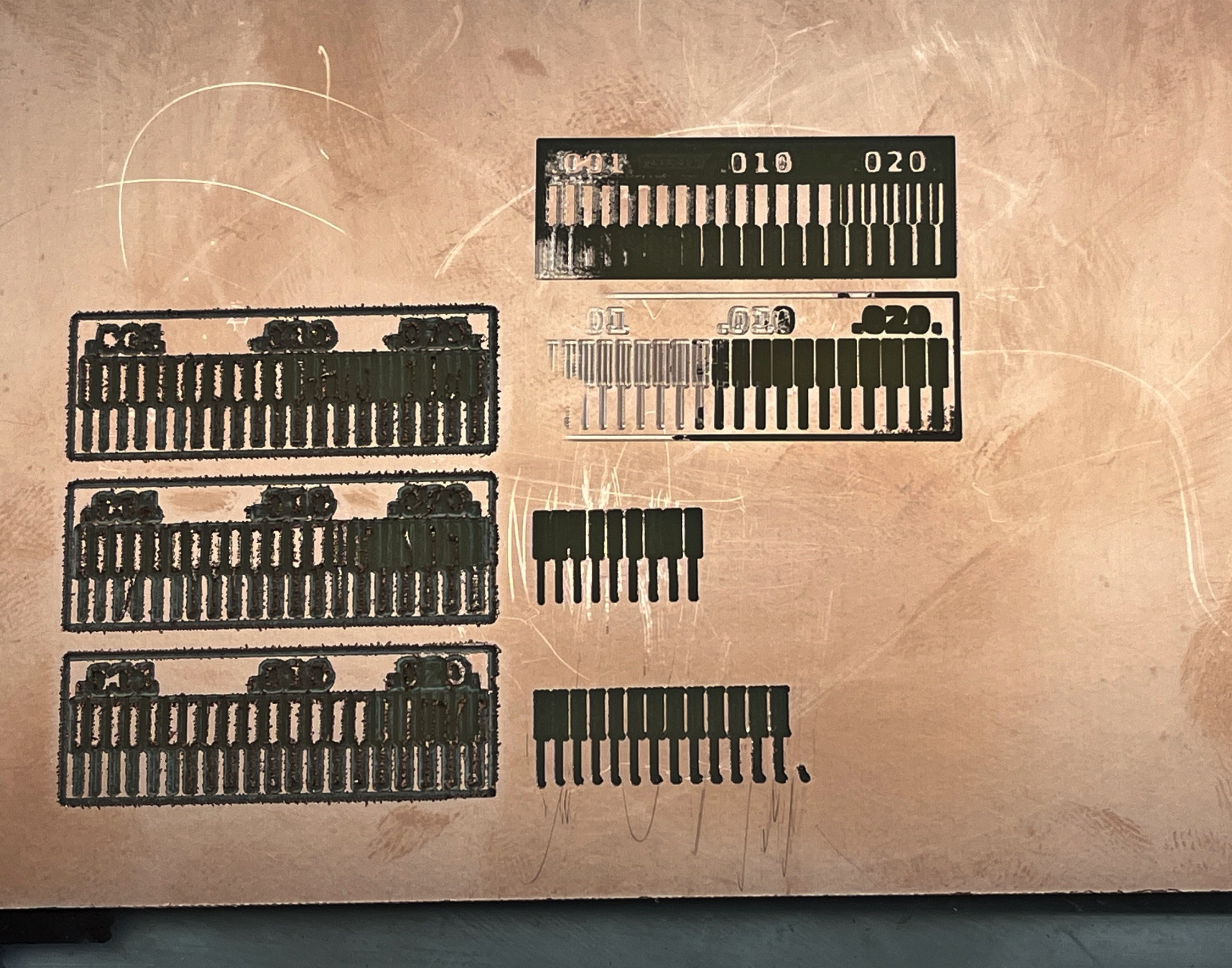
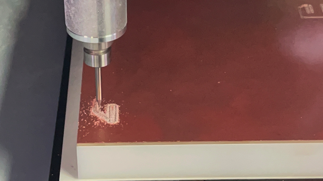
- As you will see in the images below, I eventually was able to mill the PCB but it was too small...amoung other issues.
- Along the way, I ran into many issues. These included:
- Wrong file extension type
- Material not level on milling base.
- Warped PCB blank leading to the first broken milling bit.
- Scaling issues - milled path was too small and too much copper was removed and resulted in incomplete circuit path.
- Imperial to Metric errors. - Flatcam settings were in Imperial units and MDX was in metric.
- More scaling issues - I needed to scale the Flatcam CNC output by 2.54 times to make it the correct size for the Seeed RP2040.
- Introduction
- Required Materials & Tools
- xTool F1 Ultra
- Copper-clad Fr-1 PCB board
- Safety goggles
- Proper ventilation system or exhaust fan
- Computer with xTool Creative Space application
- PCB design files
- Machine Setup
- Position Machine on a stable, flat surface
- Make sure ventilation/exhaust system is set up and running properly
- Power on & Connect to xTool
- Make sure xTool is connected to power
- Connect to xTool via Wifi or USB
- Open xTool Creative Space to make sure device is connected and ready
- Preparing the PCB board
- Surface Prep - Clean PCB using isopropyl alcohol to remove debris and oxidation.
- Secure the board in place within the engraving area
- Focusing the laser - Using the buill-in focus tool establish the laser focal length. After testiing we found that defocusing the laser my 1mm or so works best.
- Perform test engrave to ensure proper engraving depth.
- Setting Up the Deesign to be Etched
- Import Design using xTool Design Space sofwtware - (PNG or SVG)
- Position and scale the design to fit the PCB board.
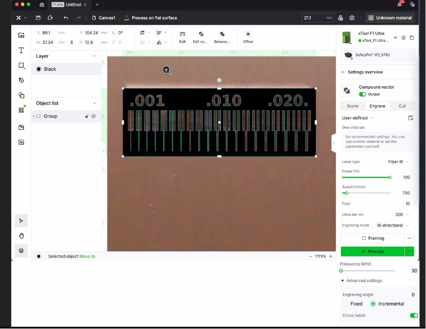
- Configrue the Laser Settings
- Select the correct material type (Copper or Custtome settings)
- Adjust power to 100%, Speed to 750mm/s, passes to 10, Lines per cm to 300
- Choose Bi-directional engrave mode
- Advanced Settings - Choose Incremental angle and Cross Hatch
- Running the Engraving Process
- Framing the Design - Use the framiing opotion to ensure the design is aligned properly on the PCB board
- Engraving the PCB - Click "Process" to start engraving
- DO NOT LEAVE THE LASER AFTER ENGRAVING STARTS
- Post_Processing
- Remove the PCB from the machine and clean the board with isopropyl alcohol to remove any residue.
- Inspect final output for accuracy and depth of cut
- Use multimeter to check for continuity
- If etching is not deep enough adjust settings and repeat
The images below represent the work above. Once we have new milling bits I will revisit this section and document how to correctly mill the PCB.
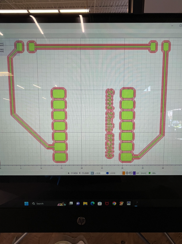
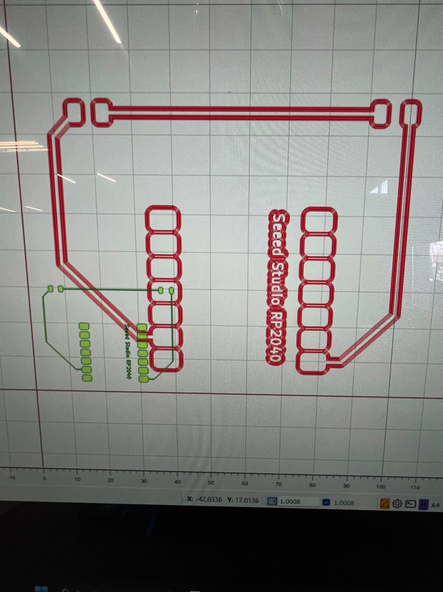
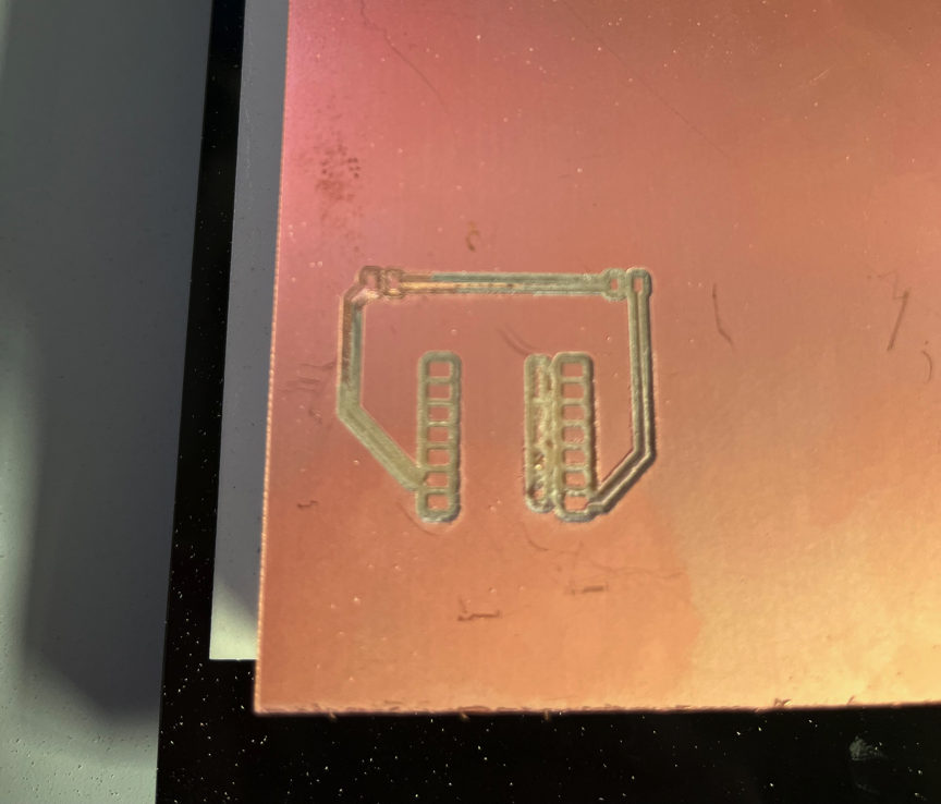
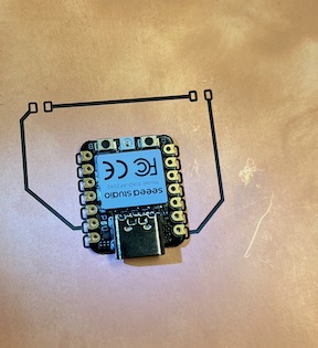
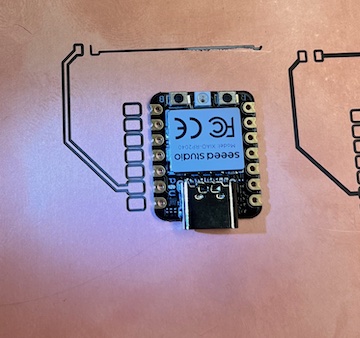
After getting the new 1/64 inch bit I was able to mill a "complete" version of my circuit, although it was not complete enough for me to cut out and solder the components on. If you look at the images below you will see that the size is correct for the RP2040 and the other components but the copper path between the connectin points was completely removed.
I was able to adjust the width of the copper path but again the board was not as level as I thought and I broke yet another bit.
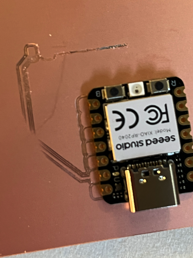
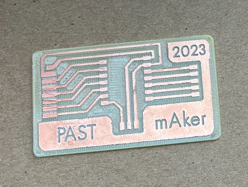
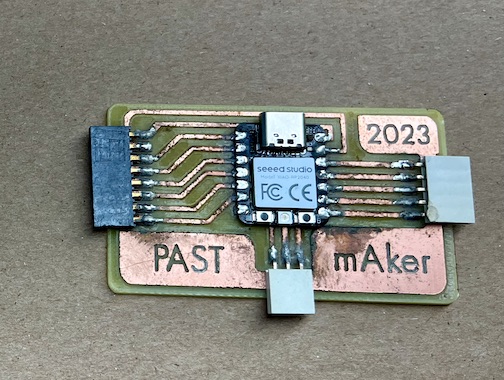
FINAL PCB Design and Fabrication
After several designs and attempts at fabrication I finally came up with a good design and used it in our summer programming. Along the way I had issues with the milling of the board but I finally go the settings (speeds and feed rates) correct and you can see in the images below that everything came out clean and neat.
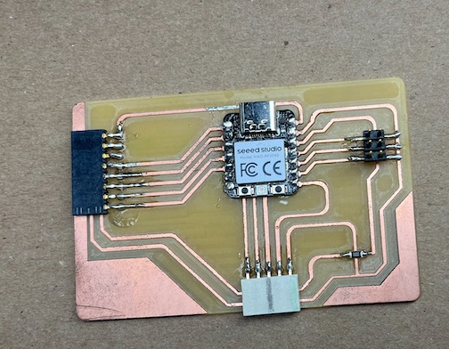
Board Built in LED Blink test
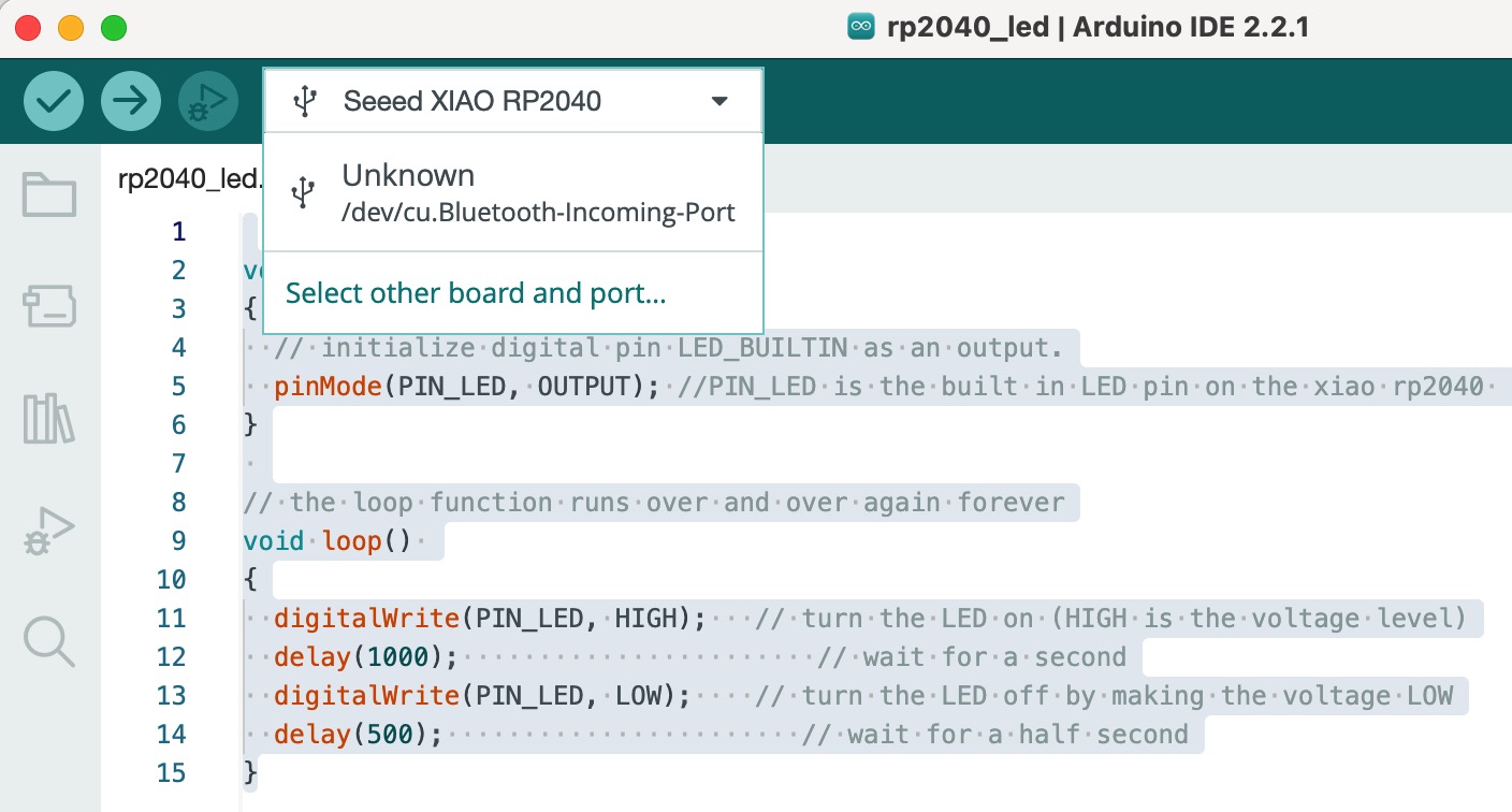
Code for built in blink. LED is on (HIGH) for 1 second and off (LOW) for one half second.
void setup()
{
  // initialize digital pin LED_BUILTIN as an output.
  pinMode(PIN_LED, OUTPUT); //PIN_LED is the built in LED pin on the xiao rp2040
}

// the loop function runs over and over again forever
void loop()
{
  digitalWrite(PIN_LED, HIGH);   // turn the LED on (HIGH is the voltage level)
  delay(1000);                       // wait for a second
  digitalWrite(PIN_LED, LOW);    // turn the LED off by making the voltage LOW
  delay(500);                       // wait for a half second
}
Unfortunately, I am having trouble connecting any of the boards I created to Arduino IDE. Sometimes I can select the board so I can upload code and many other times I can't. See images below video
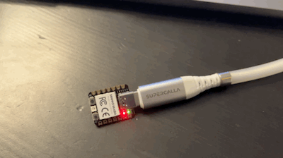
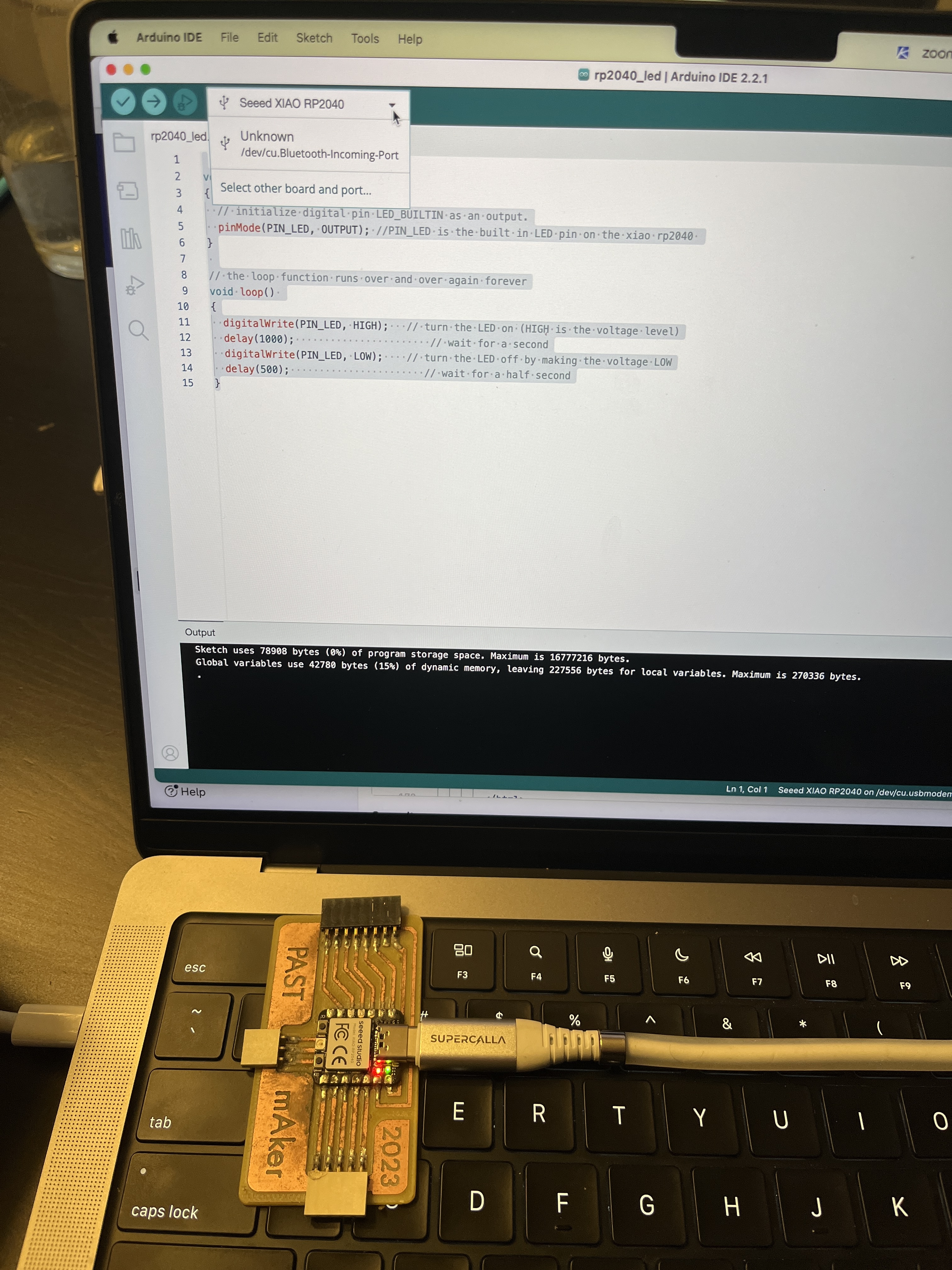
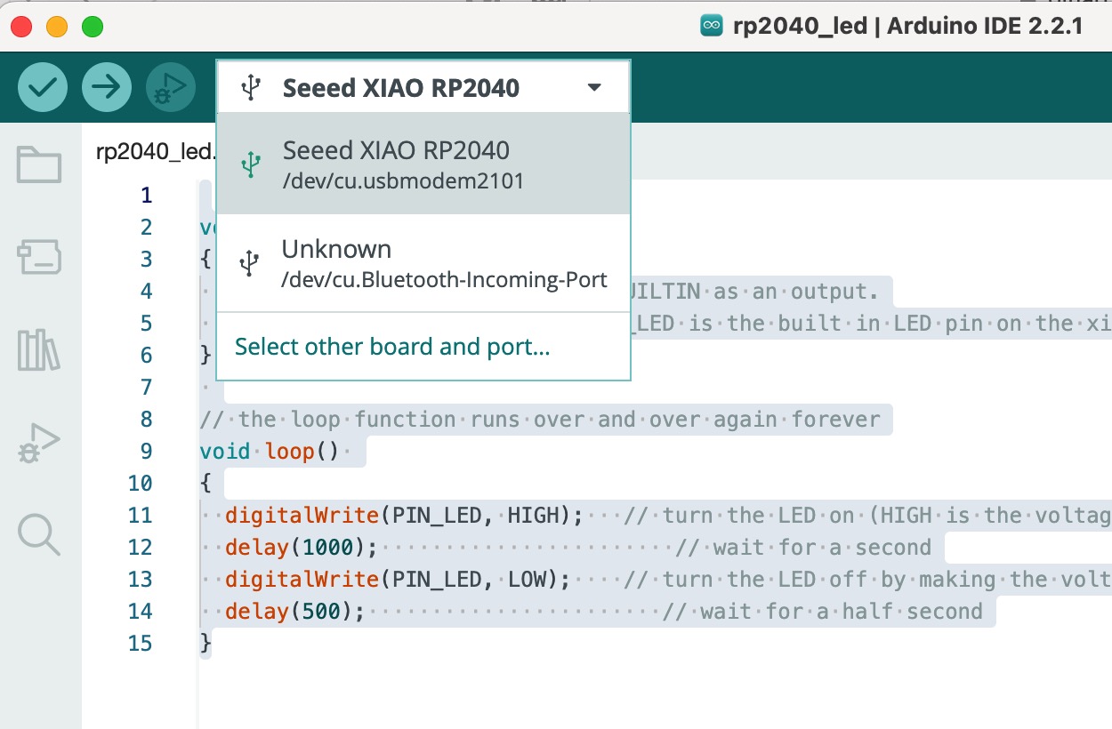
I was able to connect with a new USB-C cable and a usb hub on my MacBook. Below is the code and video for an LED blinking using a RP2040 board I made.
void setup()
  {
    // initialize digital pin D6 as an output
    pinMode(D6, OUTPUT);
  }

  // the loop function runs over and over again forever
  void loop()
  {
    digitalWrite(D6, HIGH);   // turn the LED on (HIGH is the voltage level)
    delay(1000);                       // wait for a second
    digitalWrite(D6, LOW);    // turn the LED off by making the voltage LOW
    delay(500);                       // wait for a half second
    digitalWrite(D6, HIGH);   // turn the LED on (HIGH is the voltage level)
    delay(1000);                       // wait for a second
    digitalWrite(D6, LOW);    // turn the LED off by making the voltage LOW
    delay(500);                       // wait for a half second
    digitalWrite(D6, HIGH);   // turn the LED on (HIGH is the voltage level)
    delay(1000);                       // wait for a second
    digitalWrite(D6, LOW);    // turn the LED off by making the voltage LOW
    delay(500);
  }
Project Files
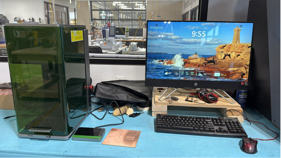
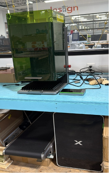
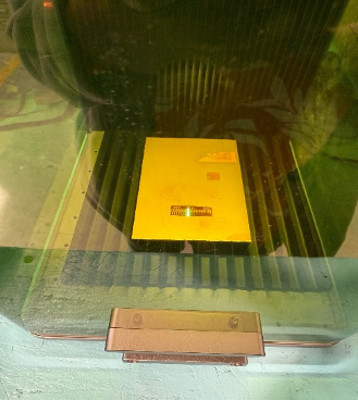
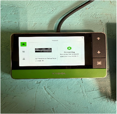
2025 Experimenting with the XTool F1 Ultra
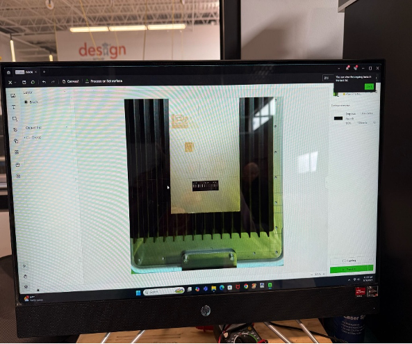
We recently added the XTool F1 Ultra to our Fab Lab. The F1 Ultra has a 20W fiber laser as well as a 20 diode laser. The fiber laser allows for etching and cutting of some metals. I was hoping that the F1 Ultra could be used to etch PCB's but after some testing I have found that it does etch the copper layer but milling may still be better. Below are some inmages and video clips of some attempts.
Update to xTool F1 Ultra
Step-by-Step Guide to Engraving PCB Boards with xTool F1 Ultra
Engraving PCB boards using the xTool F1 Ultra fiber laser engraver requires careful setup and configuration to ensure precise results. This guide provides a step-by-step process to achieve high-quality engravings.