
Assignment#4: Electronics Production
This assignment is about documenting what I learned in Electronics Production that includes PCB fabrication processes, PCB material, components, PCB assembly (including processes and tools). I have also documented how I used machining and assembly processes for PCB, tools, what precautions need to be taken while operating the milling machine, soldering station, vinyl cutter, etc. I am also documenting what I learned in programming the FabISP programmer. I fabricated flex vinyl circuit to set machine parameters like cutting force and speed. However, I could not assemble components on this PCB. I will definitely be going to make one in coming two weeks, so I am excited to do and learn PCB making for developing electronics required for my final project. I am also documenting what went well, what went wrong, how I would do things differently in next assignment and my learning outcomes.
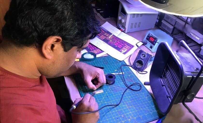
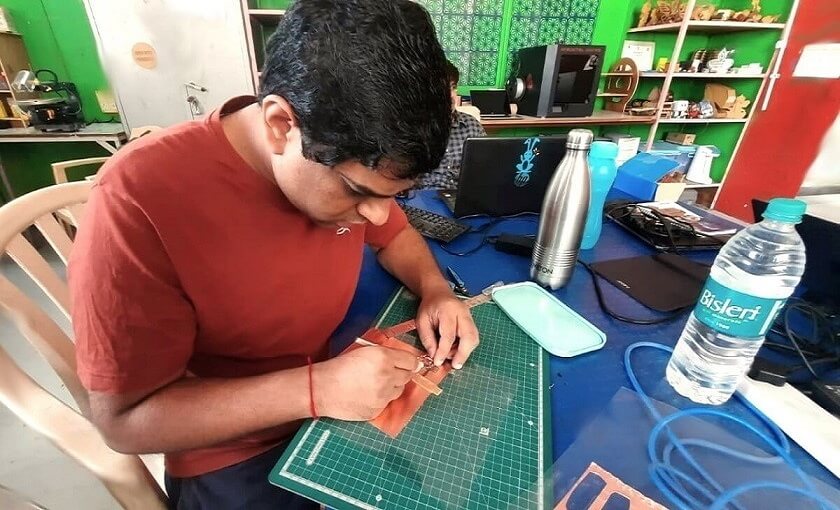
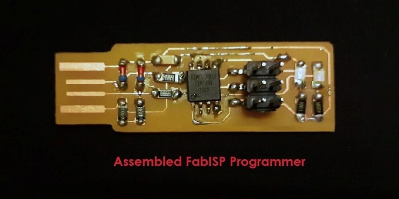
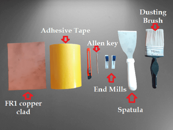
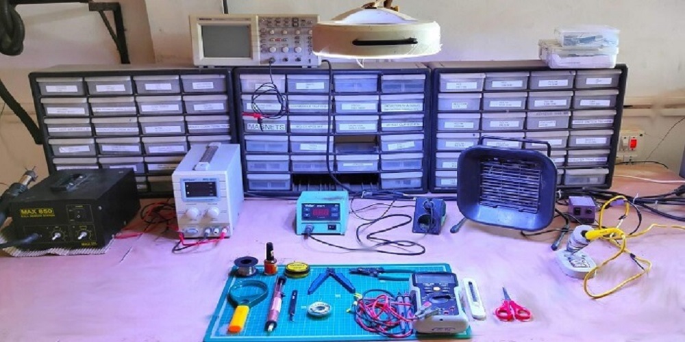
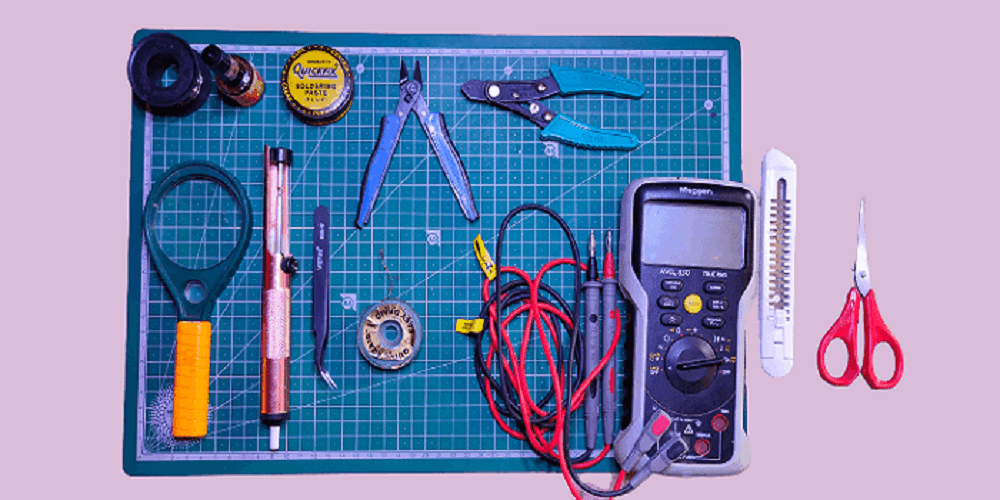
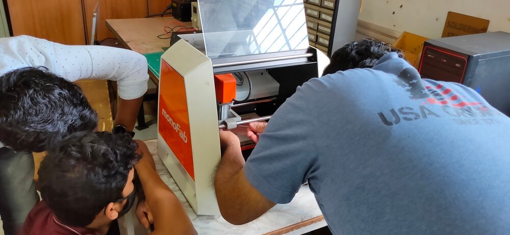
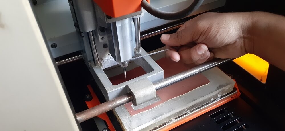
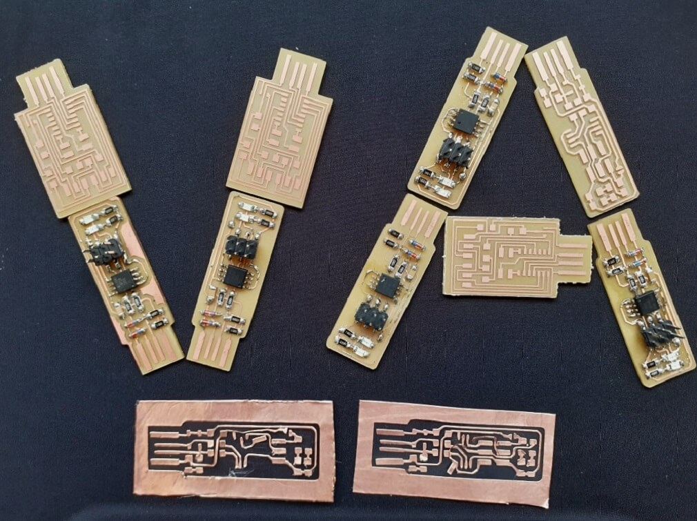
My Hero shots for this week
A. PCB Fabrication (Process, Material, Machine and Tools)
In this section, I am documenting different processes for PCB fabrication and required PCB material, machines and tools.
1. Etching for PCB Fabrication
It is traditionally the process of using strong acid or mordant to cut into the unprotected parts of a metal surface to create a design in intaglio (incised) in the metal. In modern manufacturing, other chemicals may be used on other types of material. As a method of printmaking, it is, along with engraving, the most important technique for old master prints, and remains in wide use today. In a number of modern variants such as microfabrication etching and photochemical milling it is a crucial technique in much modern technology, including circuit boards. Click here to read more.
Some of the possible weak Acids & Chemicals used in Etching
- Acetic acid = CH3COOH (also written as CH3CO2H or C2H4O2) White Vinegar
- Citric acid = C6H8O7 Sour Salt dry powdered form
- Hydrochloric acid / Muriatic acid = HCl Swimming Pools to reduce alkalinity
- Hydrogen Peroxide = H2O2 First Aid Antiseptic Solution, & Mild Disinfectant for wounds
- Sodium chloride = NaCl The chemical name for Salt
- Copper sulfate = CuSO4
Precautions to be taken in Etching
- Waste management- Once all the unmasked copper has been etched away, take out and rinse off the board with running water. The remaining blue solution will contain dissolved copper salts which are not environmentally friendly and very toxic to plant and aquatic life.
-Reusing etching solution- Reusing the etching solution is not favored because it results in slower and more messier process. Using fresh mix every time is preferable.
-Neutralizing the acid & precipitating the Copper- Adding sodium bicarbonate (baking soda) in small amounts at a time; the solution will fizz and release carbon dioxide gas. This will neutralize the citric acid, and precipitate out the copper in the form of copper carbonates. The solution is sufficiently neutralized when no more fizzing occurs on bicarbonate addition. At this point the liquid can be safely disposed of (down the drain in small amounts), and the left over precipitant can be disposed of as solid waste (in the garbage). Click here to read more.
2. Machining (Milling) for PCB Fabrication
Printed circuit board milling (also: isolation milling) is the process of removing areas of copper from a sheet of printed circuit board material to recreate the pads, signal traces and structures according to patterns from a digital circuit board plan known as a layout file. Similar to the more common and well known chemical PCB etch process, the PCB milling process is subtractive: material is removed to create the electrical isolation and ground planes required. However, unlike the chemical etch process, PCB milling is typically a non-chemical process and as such it can be completed in a typical office or lab environment without exposure to hazardous chemicals. High quality circuit boards can be produced using either process. In the case of PCB milling, the quality of a circuit board is chiefly determined by the system's true, or weighted, milling accuracy and control as well as the condition (sharpness, temper) of the milling bits and their respective feed/rotational speeds. By contrast, in the chemical etch process, the quality of a circuit board depends on the accuracy and/or quality of the mask used to protect the copper from the chemicals and the state of the etching chemicals. Click here to read more.
Material, Machine and Tools used in PCB Machining (Milling)
Material:
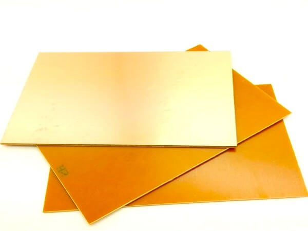
- FR1-Phenolic paper is a material often used to make printed circuit board substrates (the flat board to which the components and traces are attached). It is a very tough board made of wood fibre and phenolic polymers. It is most commonly brown in colour, and is a fibre reinforced plastic. These PCB materials are known as FR-1 and FR-2.
- Epoxy Film Electrical Tape with Thermosetting Acrylic Adhesive
- Electronic componets
Machine:
- The mechanics behind a PCB milling machine are fairly straightforward and have their roots in CNC milling technology. A PCB milling system is similar to a miniature and highly accurate NC milling table. For machine control, positioning information and machine control commands are sent from the controlling software via a serial port or parallel port connection to the milling machine's on-board controller. The controller is then responsible for driving and monitoring the various positioning components which move the milling head and gantry and control the spindle speed.
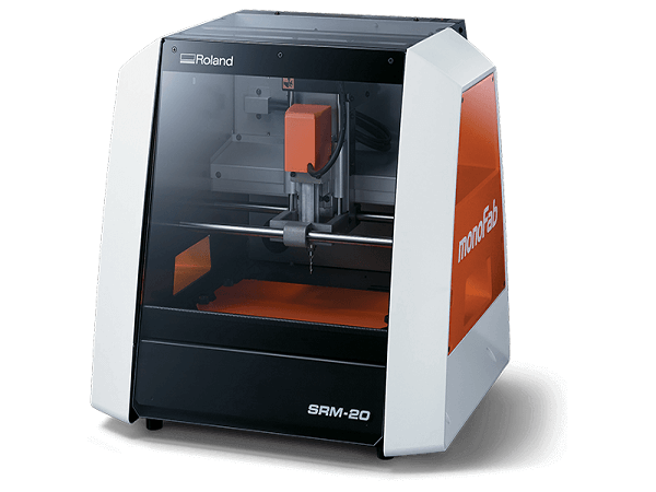
- e.g. Roland SRM-20 is a precision three-axis machining, including PCBs down to 0.25 mm feature size, and machineable wax to make tooling for molding and casting
Tools:
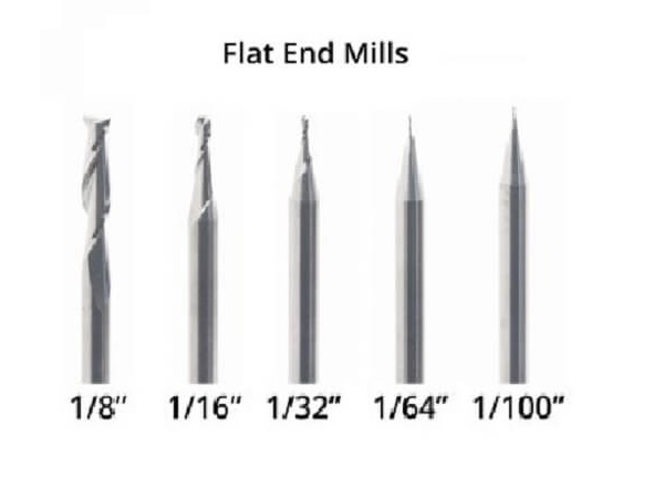
- PCBs can be machined with conventional endmills. Flat end mills have many advantages. Their straight profiles and consistent diameters ensure that milled traces are of a consistent width, even if the FR-1 PCB blank used is not perfectly flat. Flat end mills are also great at clearing large areas of material, and large flat end mills can remove material very quickly.
 |
 |
 |
 |
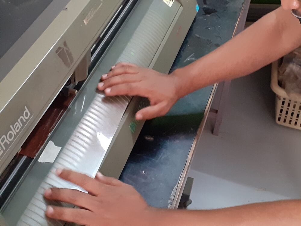
3. Vinyl cutting for flexible PCB Fabrication
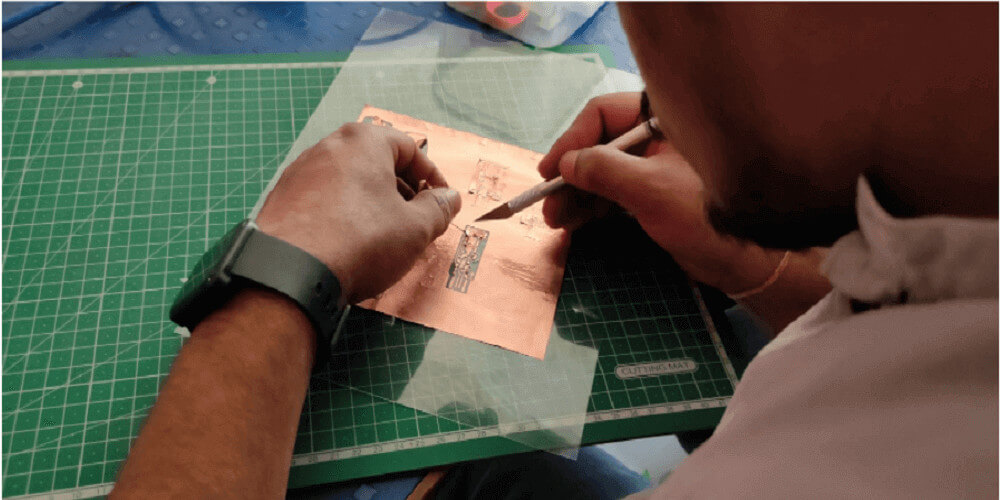
Making flexible PCBs is easier than most of the people may think. They are used in applications such as wearables or flexible and small mechanism where PCB has to be embedded. We use a vinyl cutter to cut the traces of a circuit design out of copper foil with adhesive backing. The copper traces can then be transferred to a base to make a flexible circuit. Additionally, a solder mask can be laser cut (or also vinyl cut) from non-conductive material with adhesive backing and applied to isolate the traces and only expose the copper where one needs access to solder the components. Click here to read more.
Material, Machine and Tools used in Vinyl cutting
Material:
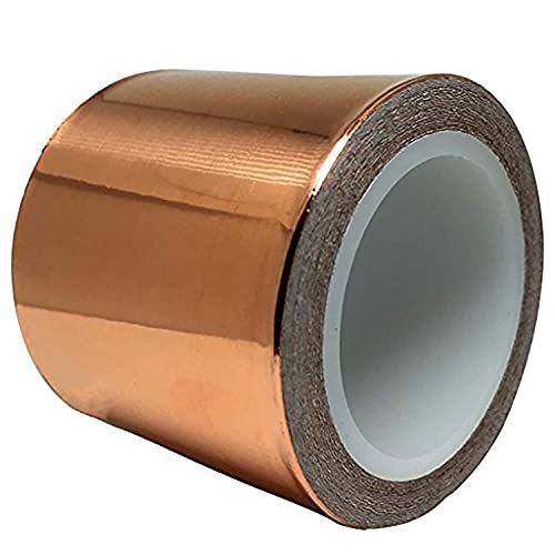
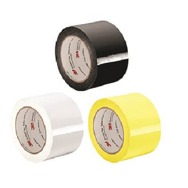
- 3M Copper Foil Tape 1126
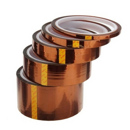
- Kapton tape is a thin, flexible polyimide film used in flexible printed circuits (flexible electronics) and space blankets, which are used on spacecraft, satellites, and various space instruments. Discovered by the DuPont Corporation in the 1960s, Kapton remains stable (in isolation) across a wide range of temperatures, from 4 to 673 K (- 269 to +400 deg C). Kapton Tape is not obligatory but highly recommended,as it will protect your PVC sheet from overheating while your solder the electronic components.
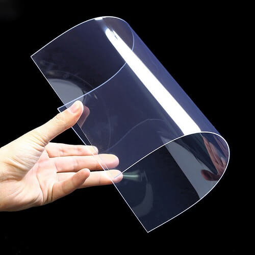
- For Flexible Support, we used a thin PVC sheet used in OHP
- 3M Epoxy Film Electrical Tape 1 with Thermosetting Acrylic Adhesive
- Electronic components for your board
Machine:
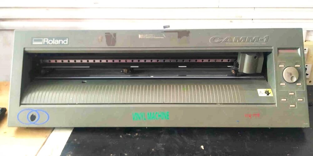
- A vinyl cutter that is mostly used for making signs can be used to cut the flexible circuits on the kapton tape. To know more about vinyl cutter, click here to visit the company website.
- The CX-12/24 is exceptionally easy to use and incorporates advanced features previously available only on Rolands PRO series vinyl cutters.
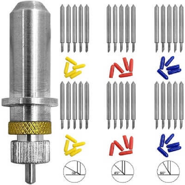
Tools:
Below are some of the types of blades used in vinyl cutting
- 30 deg blade is used for very thin material.
- 45 deg blade is used for general vinyl cutter.
- 60 deg blade is suit for thick material like copper sheet, mirror sheet, sand blast regist sheet.
 |
 |
 |
 |
 |
 |
 |
Click here to go back to the top
B. PCB components and assembly
In this section, I am documenting different types of electronics components used in PCBs along with processes and tools required in PCB assembly.
Types of PCB components:
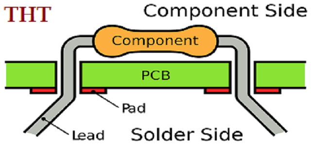
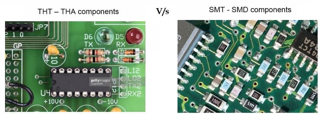
1. Through-hole technology
The first PCBs used through-hole technology, mounting electronic components by leads inserted through holes on one side of the board and soldered onto copper traces on the other side. Boards may be single-sided, with an unplated component side, or more compact double-sided boards, with components soldered on both sides. Horizontal installation of through-hole parts with two axial leads (such as resistors, capacitors, and diodes) is done by bending the leads 90 degrees in the same direction, inserting the part in the board (often bending leads located on the back of the board in opposite directions to improve the part's mechanical strength), soldering the leads, and trimming off the ends. Leads may be soldered either manually or by a wave soldering machine.
Through-hole manufacture adds to board cost by requiring many holes to be drilled accurately, and it limits the available routing area for signal traces on layers immediately below the top layer on multi-layer boards, since the holes must pass through all layers to the opposite side. Once surface-mounting came into use, small-sized SMD components were used where possible, with through-hole mounting only of components unsuitably large for surface-mounting due to power requirements or mechanical limitations, or subject to mechanical stress which might damage the PCB (e.g. by lifting the copper off the board surface). Click here to read more.
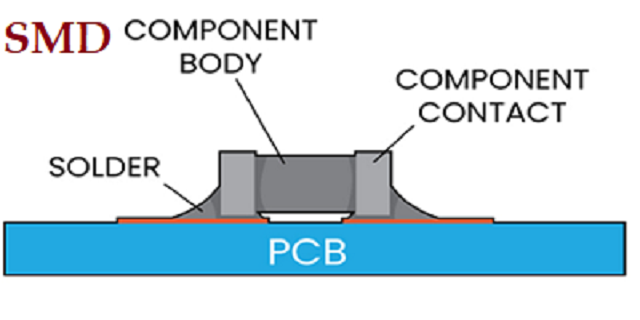
2. Surface-mount technology
Surface-mount technology emerged in the 1960s, gained momentum in the early 1980s, and became widely used by the mid-1990s. Components were mechanically redesigned to have small metal tabs or end caps that could be soldered directly onto the PCB surface, instead of wire leads to pass through holes. Components became much smaller and component placement on both sides of the board became more common than with through-hole mounting, allowing much smaller PCB assemblies with much higher circuit densities. Surface mounting lends itself well to a high degree of automation, reducing labor costs and greatly increasing production rates compared with through-hole circuit boards. Components can be supplied mounted on carrier tapes. Surface mount components can be about one-quarter to one-tenth of the size and weight of through-hole components, and passive components much cheaper. However, prices of semiconductor surface mount devices (SMDs) are determined more by the chip itself than the package, with little price advantage over larger packages, and some wire-ended components, such as 1N4148 small-signal switch diodes, are actually significantly cheaper than SMD equivalents. Click here to read more.
Below is a picture highlighting the difference between through-hole technology versus surface-mount technology.
 |
 |
 |
PCB assembly
In assembly the bare board is populated (or "stuffed") with electronic components to form a functional printed circuit assembly (PCA), sometimes called a "printed circuit board assembly" (PCBA). In through-hole technology, the component leads are inserted in holes surrounded by conductive pads; the holes keep the components in place. In surface-mount technology (SMT), the component is placed on the PCB so that the pins line up with the conductive pads or lands on the surfaces of the PCB; solder holds the components in place temporarily; if surface-mount components are applied to both sides of the board, the bottom-side components are glued to the board. In both through hole and surface mount, the components are then soldered; once cooled and solidified, the solder holds the components in place permanently and electrically connects them to the board. Click here to read more.
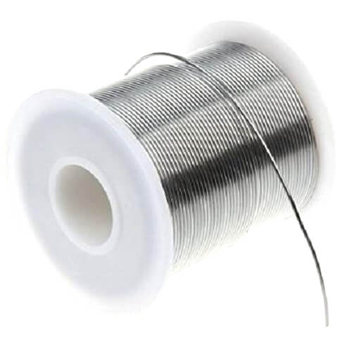
Solder is a fusible metal alloy used to create a permanent bond between metal workpieces. Solder is melted in order to adhere to and connect the pieces after cooling, which requires that an alloy suitable for use as solder have a lower melting point than the pieces being joined. The solder should also be resistant to oxidative and corrosive effects that would degrade the joint over time. Solder used in making electrical connections also needs to have favorable electrical characteristics. Click here to read more.
Types of solder (Click here to read more)
Lead-based solder- Tin-lead (Sn-Pb) solders, also called soft solders, are commercially available with tin concentrations between 5% and 70% by weight.
Lead-free solder- The European Union Waste Electrical and Electronic Equipment Directive and Restriction of Hazardous Substances Directive were adopted in early 2003 and came into effect on July 1, 2006, restricting the inclusion of lead in most consumer electronics sold in the EU, and having a broad effect on consumer electronics sold worldwide. In the US, manufacturers may receive tax benefits by reducing the use of lead-based solder. Lead-free solders in commercial use may contain tin, copper, silver, bismuth, indium, zinc, antimony, and traces of other metals.
Solder paste- Solder paste is used in the manufacture of printed circuit boards to connect surface mount components to pads on the board. It is also possible to solder through-hole pin in paste components by printing solder paste in and over the holes. The sticky paste temporarily holds components in place; the board is then heated, melting the paste and forming a mechanical bond as well as an electrical connection. The paste is applied to the board by jet printing, stencil printing or syringe; then the components are put in place by a pick-and-place machine or by hand. Click here to read more.
 |
 |
Solder flux- Flux is a chemical cleaning agent used before and during the soldering process of electronic components onto circuit boards. Flux is used in both manual hand soldering as well as the different automated processes used by PCB contract manufacturers. The main purpose of the flux is to prepare the metal surfaces for soldering by cleaning and removing any oxides and impurities. Oxides are formed when metal is exposed to air and may prevent the formation of good solder joints. The flux also protects the metal surfaces from re-oxidation during soldering and helps the soldering process by altering the surface tension of the molten solder. Click here to read more. Flux comes in semi-solid or liquid form as shown in images below.
 |
 |
Desoldering In electronics, desoldering is the removal of solder and components from a circuit board for troubleshooting, repair, replacement, and salvage. Click here to read more
Desoldering tools and materials include the following:
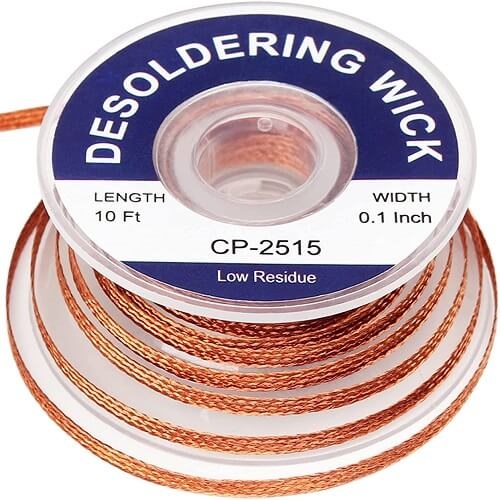
Desoldering braid- Desoldering braid, also known as desoldering wick or solder wick, is finely braided 18 to 42 AWG copper wire coated with rosin flux, usually supplied on a roll. The end of a length of braid is placed over the soldered connections of a component being removed. The connections are heated with a soldering iron until the solder melts and is wicked into the braid by capillary action. The braid is removed while the solder is still molten, its used section cut off and discarded when cool. Short lengths of cut braid will prevent heat being carried away by the braid instead of heating the joint. Click here to read more.
Solder remover suction/vacuum pumps- are used to suck away molten solder, leaving previously joined terminals disconnected. They are primarily used to release through-hole connections from a PCB. Suction pumps are also used with a suction head appropriate for each part to pick up and remove tiny surface mount devices once solder has melted, and to place parts. A desoldering pump, colloquially known as a solder sucker, is a manually-operated device which is used to remove solder from a printed circuit board. Click here to read more.
 |
 |
Hot air guns- They blow air hot enough to melt all the solder around a small surface mounted part, and can be used for soldering parts in place, and for desoldering followed by removal before the solder solidifies by a vacuum pump or with tweezers. Hot air has a tendency to oxidise metals; a non-oxidising gas, usually nitrogen, can be used instead of air, at increased cost of equipment and consumables.
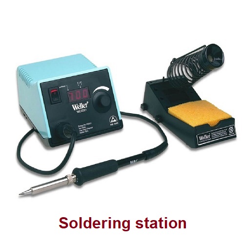
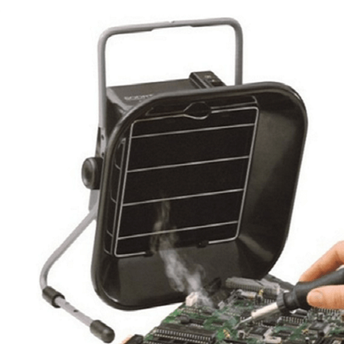
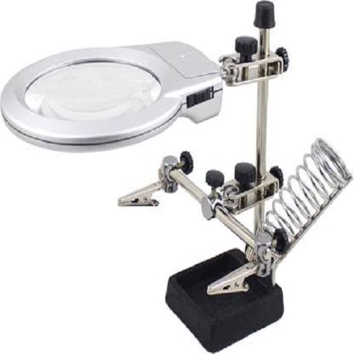
Soldering station- A soldering station is a multipurpose power soldering device designed for electronic components soldering. This type of equipment is mostly used in electronics and electrical engineering. Soldering station consists of one or more soldering tools connected to the main unit, which includes the controls (temperature adjustment), means of indication, and may be equipped with an electric transformer. Soldering stations may include some accessories like holders and stands, soldering tip cleaners, hot air gun, soldering fume extractor and magnifying glass with light, etc. Click here to read more.
 |
 |
 |
 |
Soldering station and tools at Fab Lab in Vigyan Ashram.
 |
 |
Click here to go back to the top
Group Assignment Brief
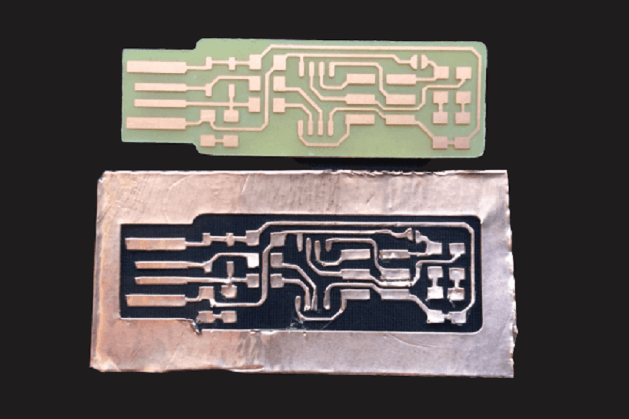
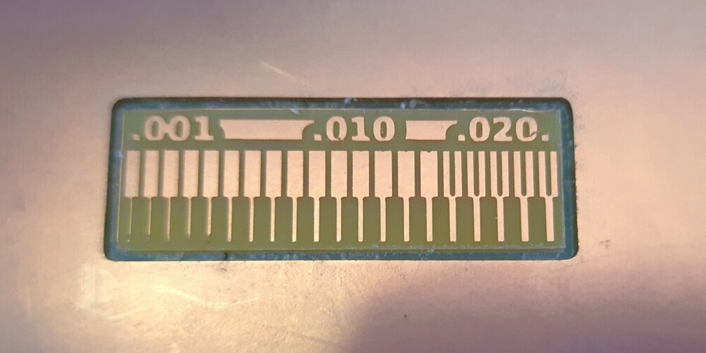
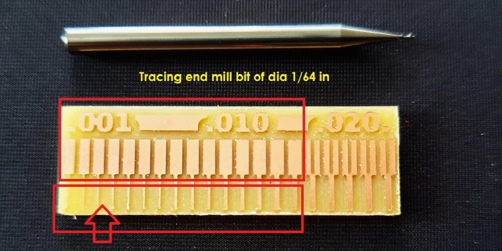
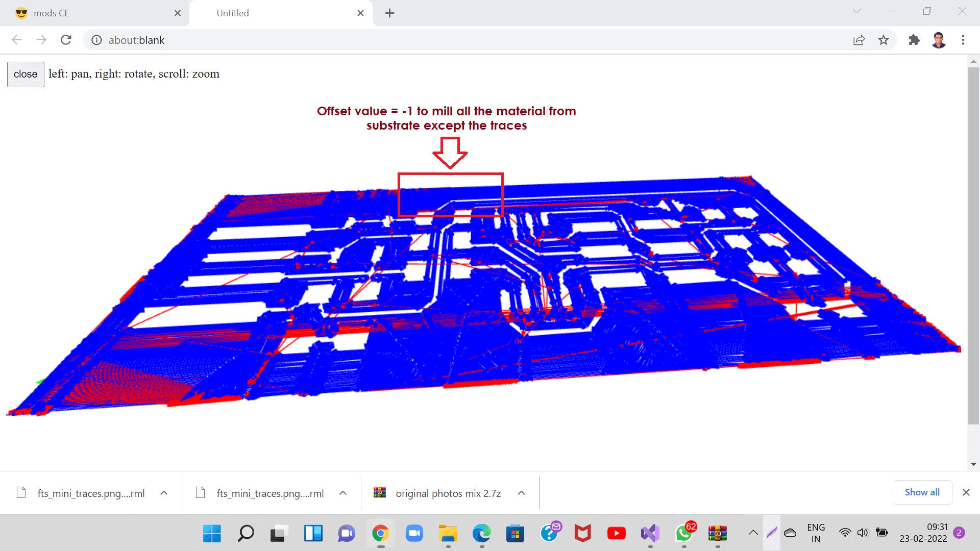
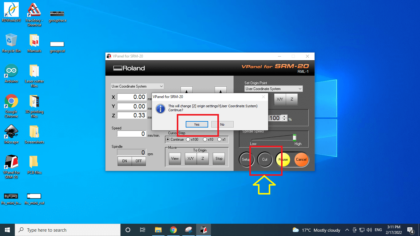
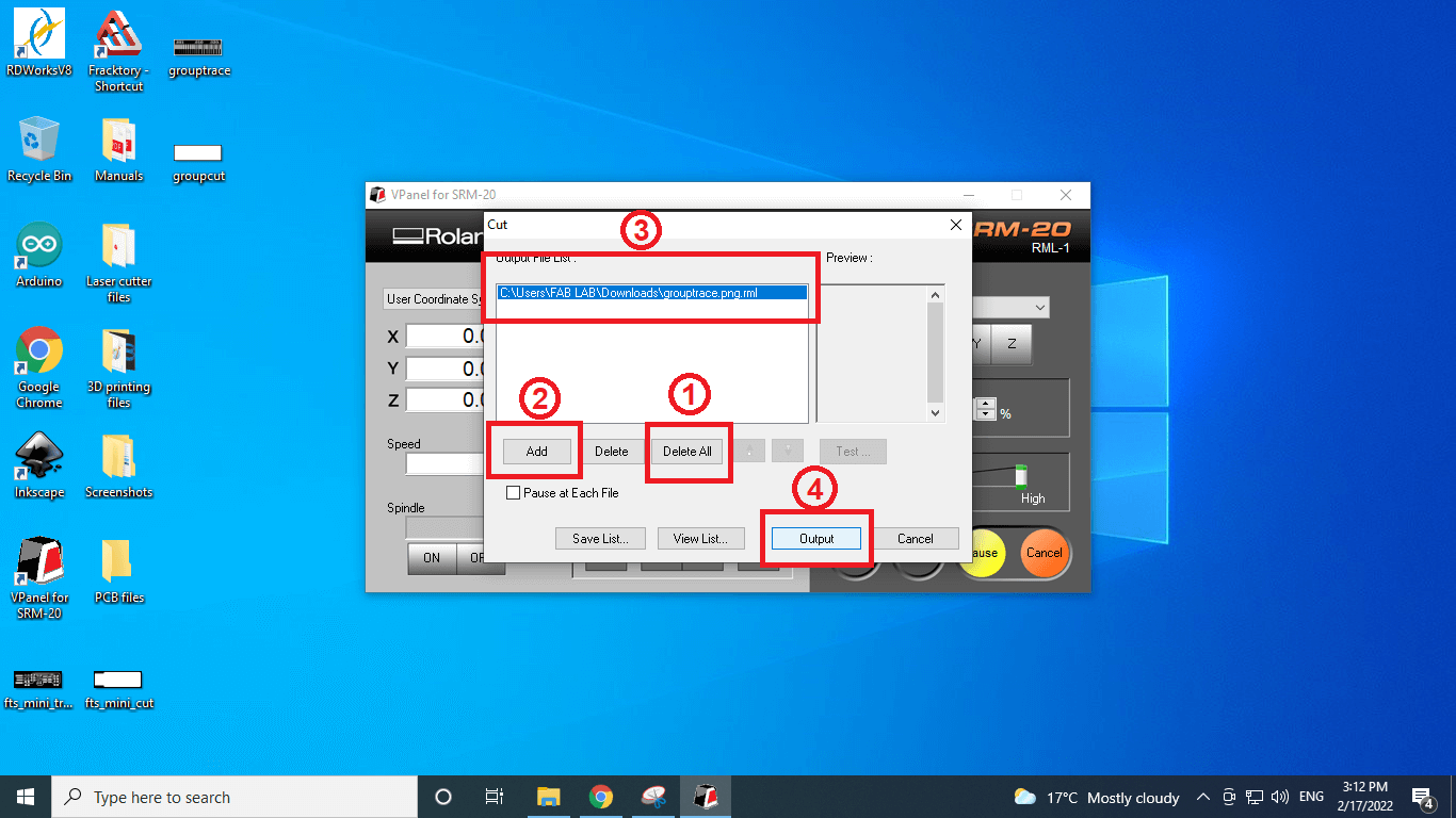
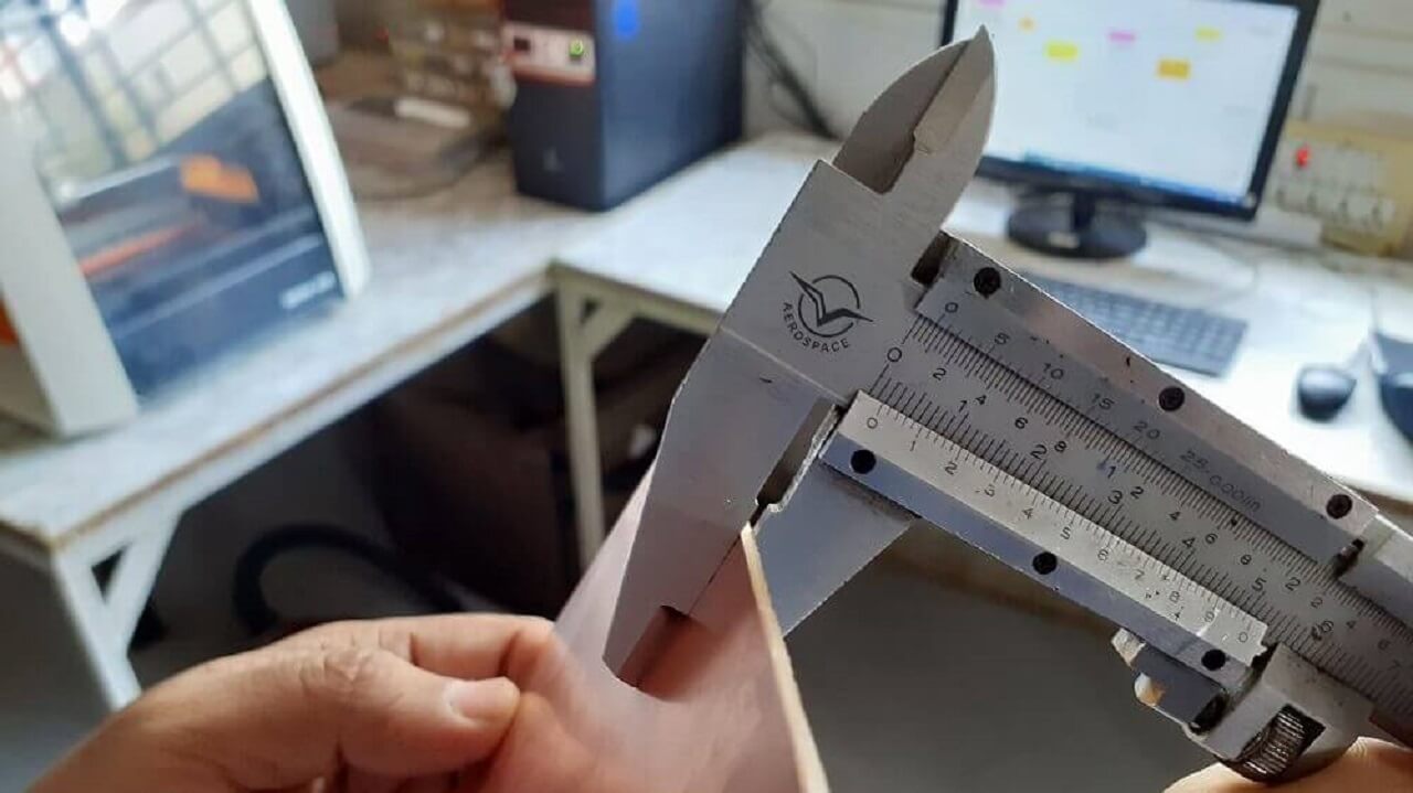
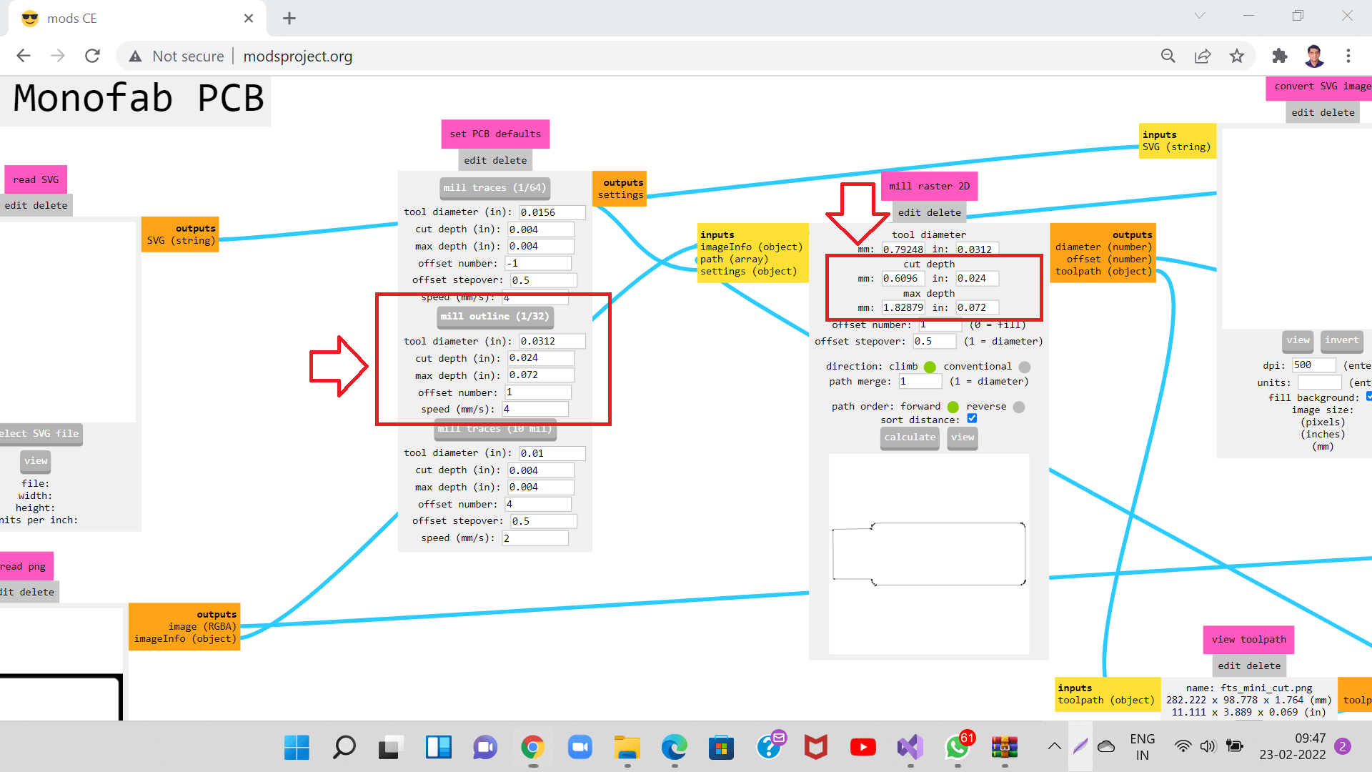
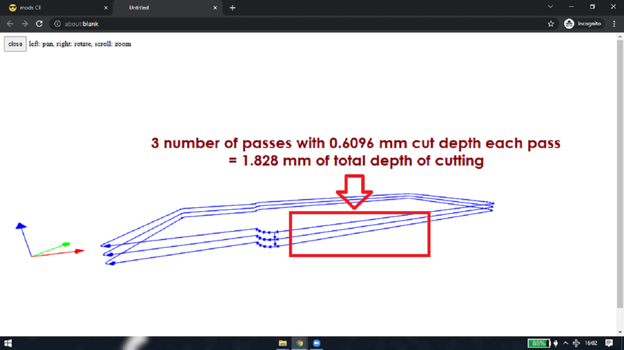
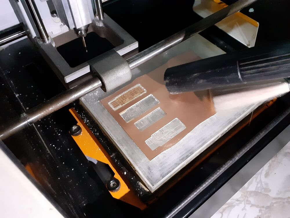
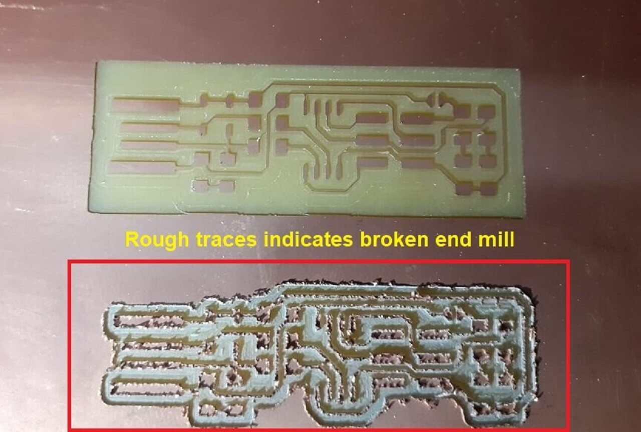
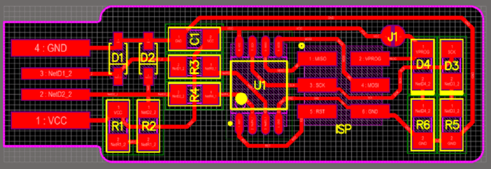
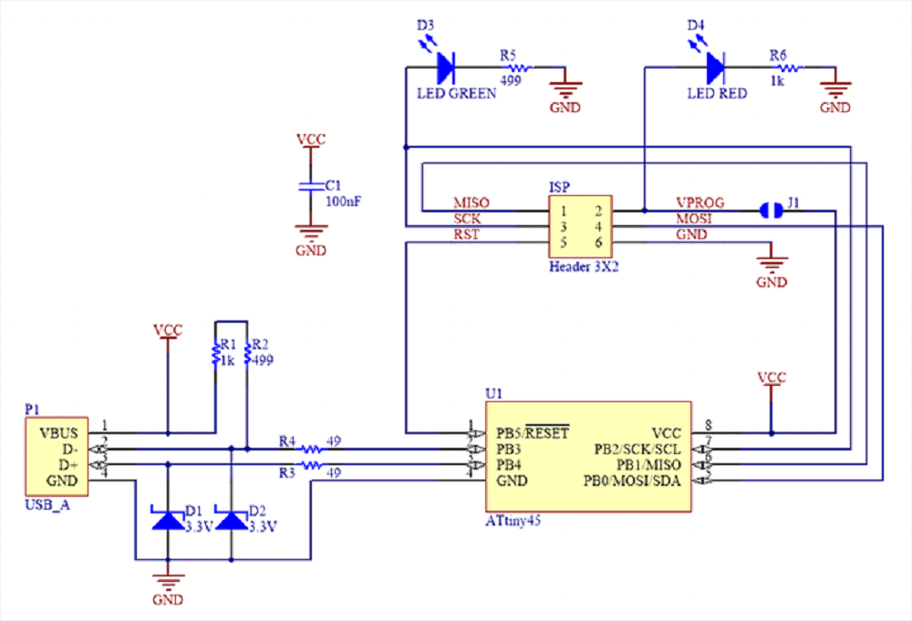
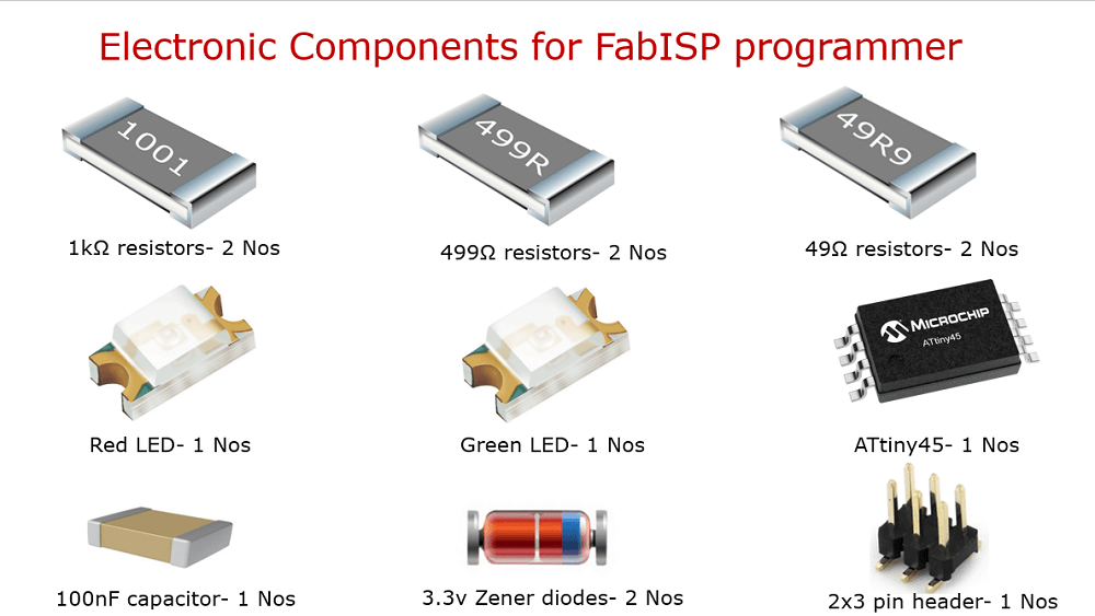
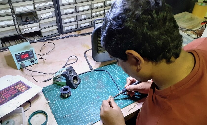
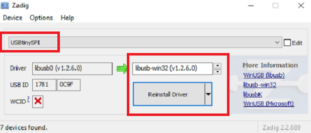
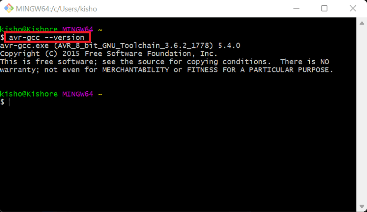
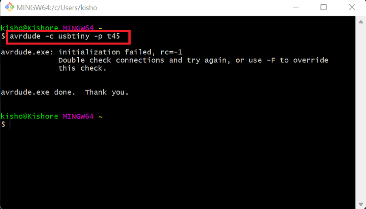
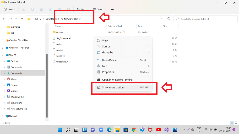
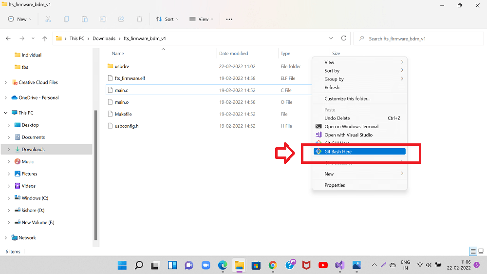
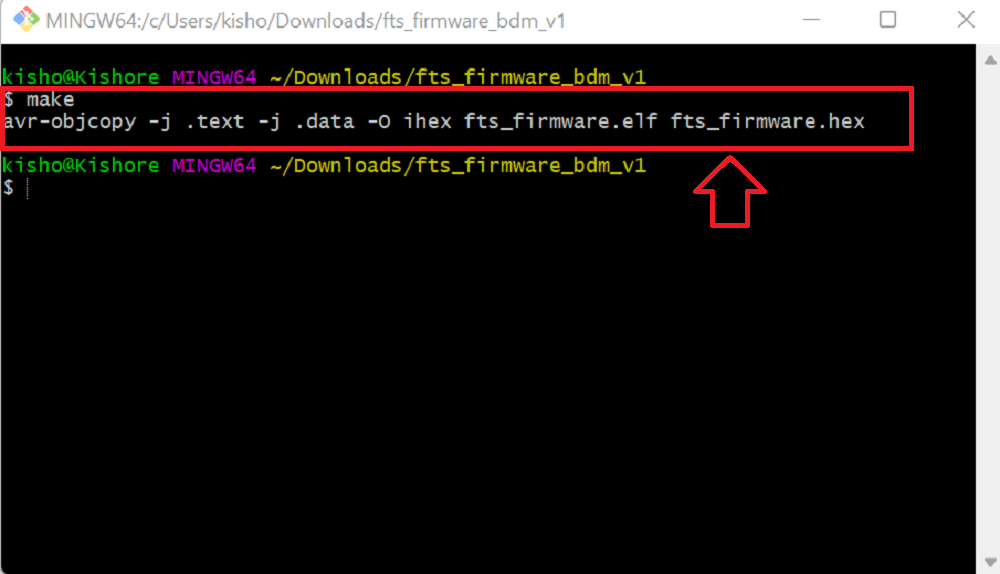
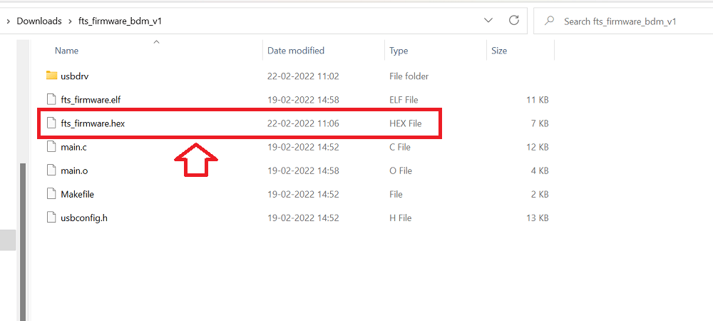
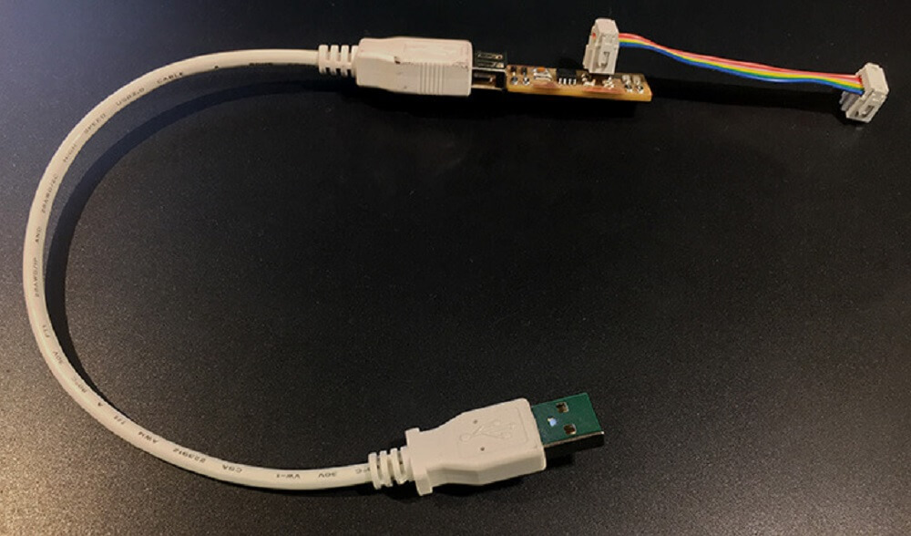
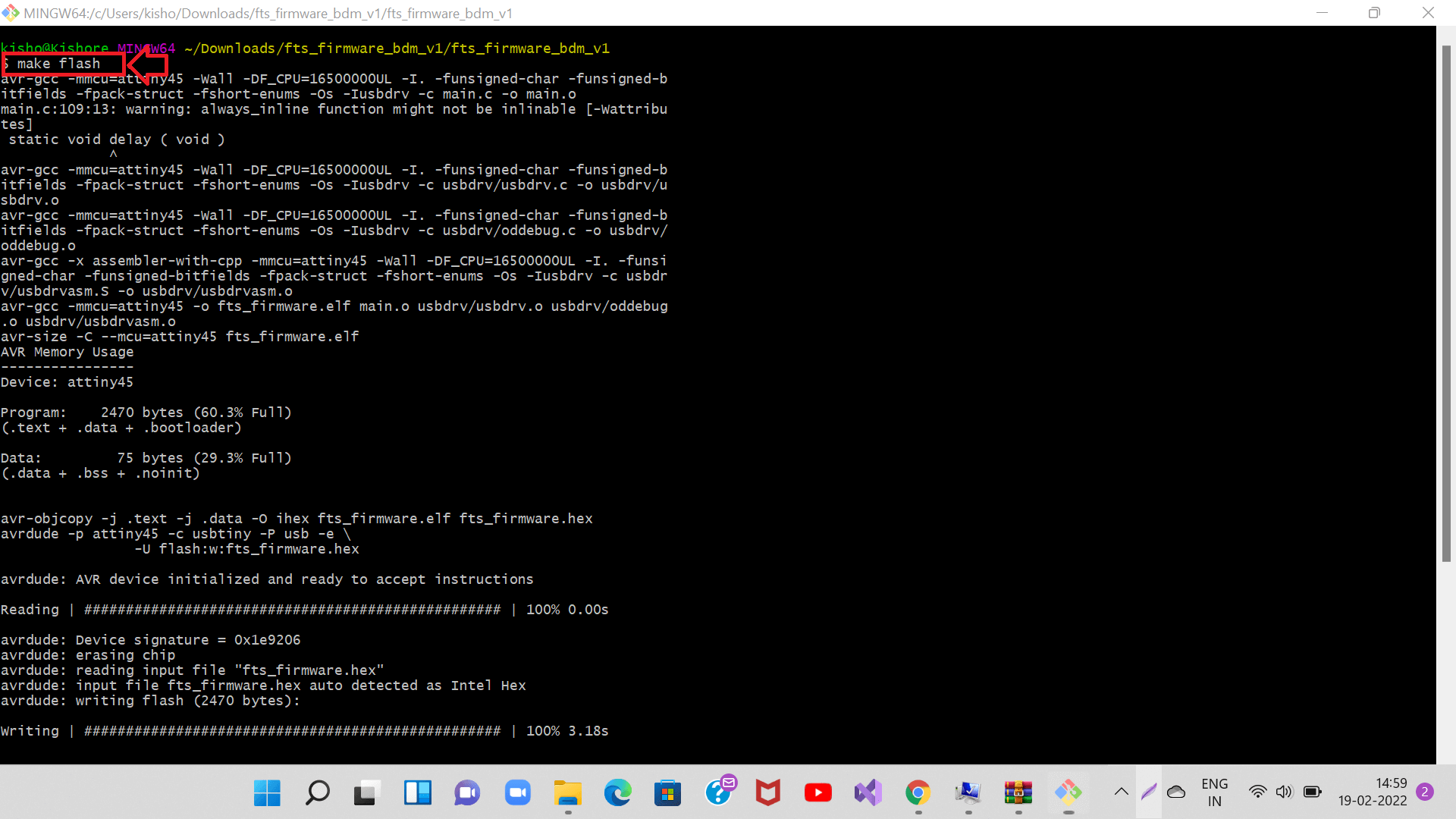
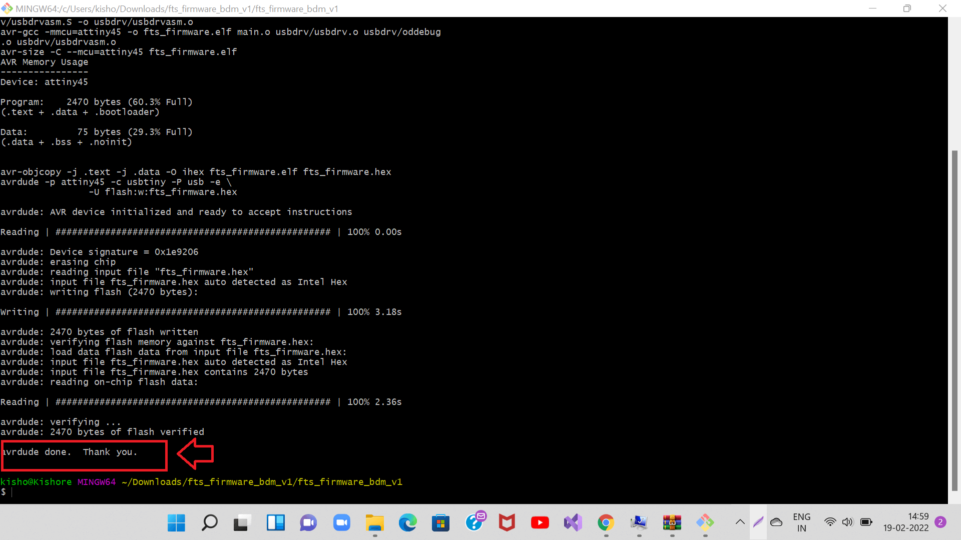
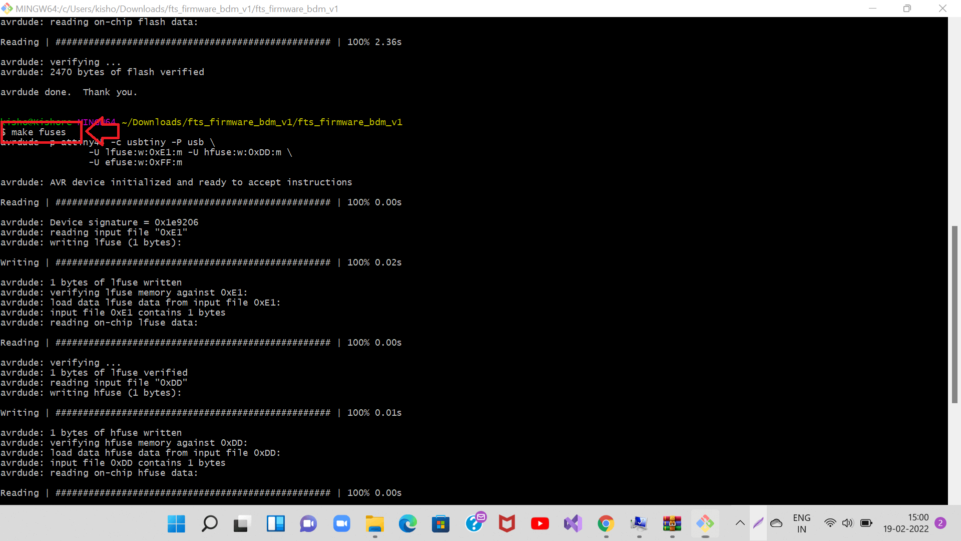
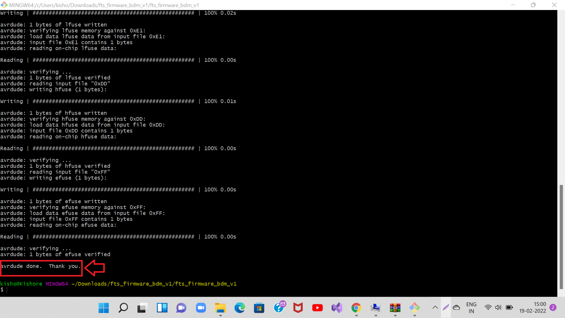
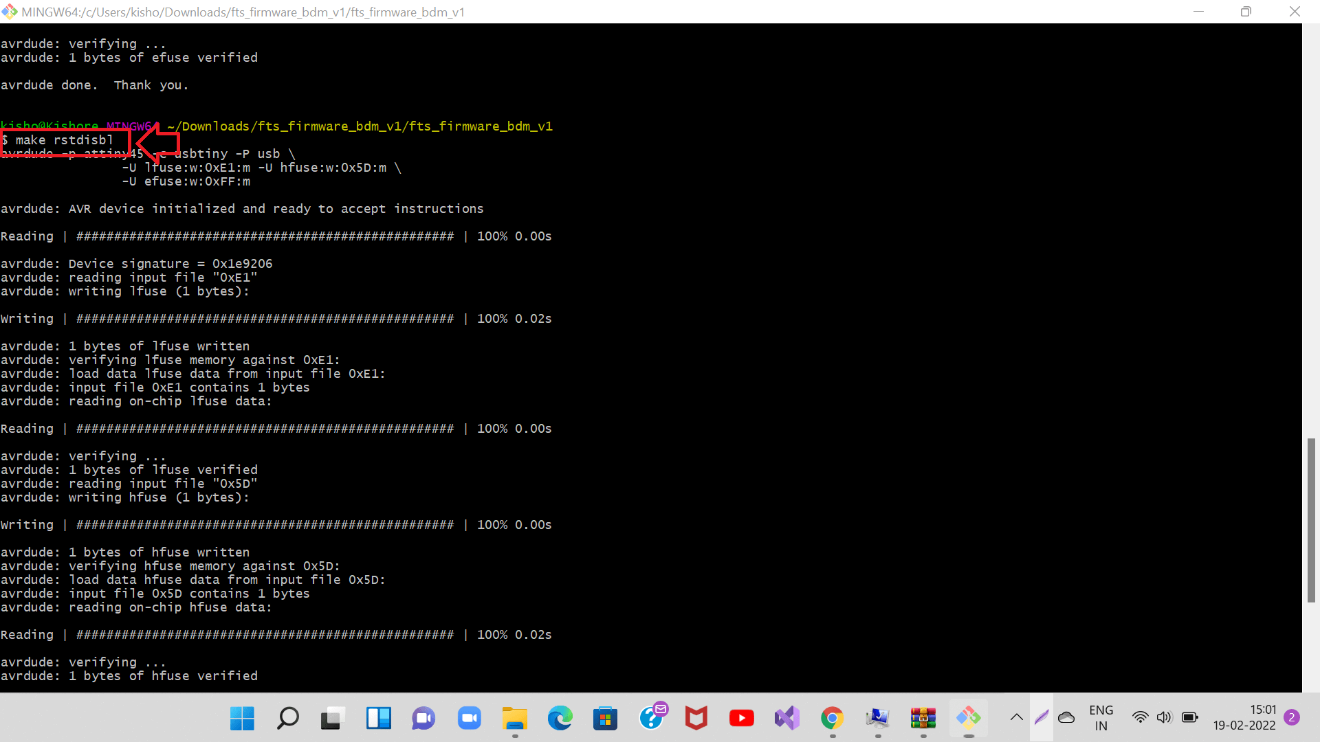
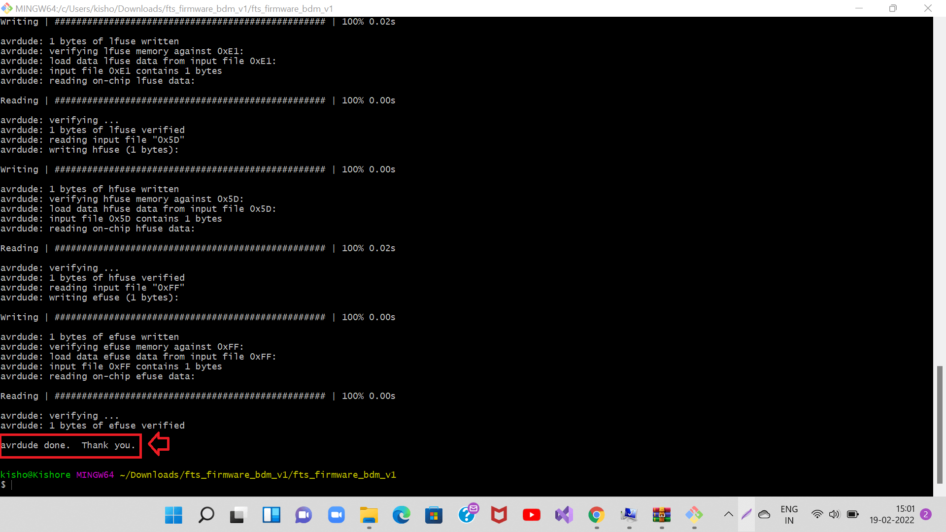
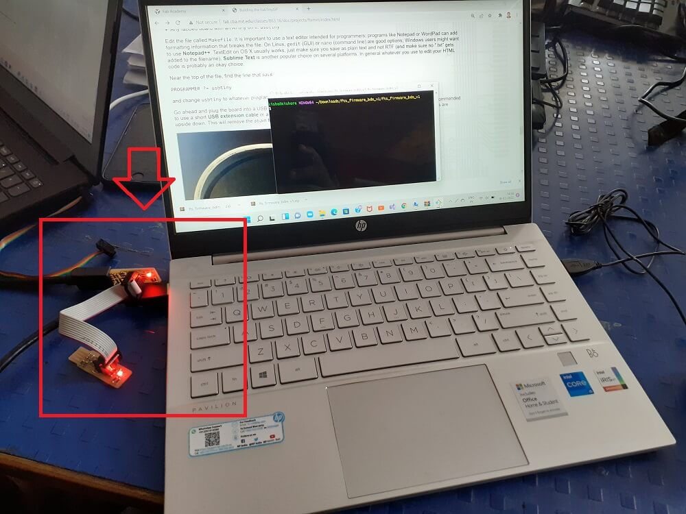
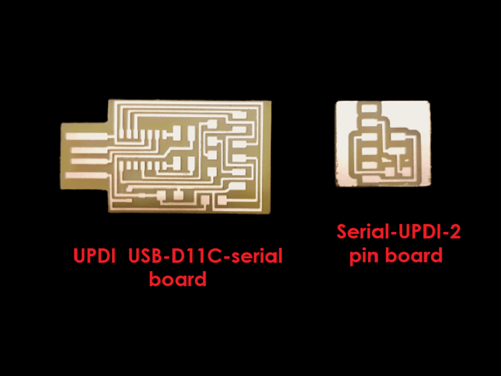
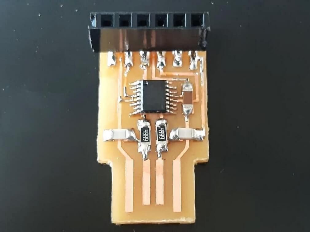
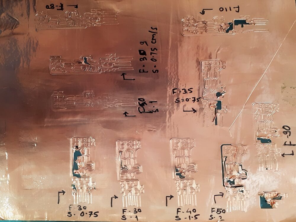
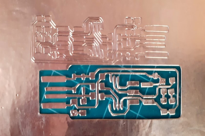
This week, we worked on Electronic Production group assignment. This assignment is about documenting what we learned in Electronics Production that includes PCB fabrication processes, PCB material, components, PCB assembly (including processes and tools). We have also documented how we used machining process for PCB, tools, what precautions need to be taken while operating the milling machine. As a conclusion we characterized the design rules for your in-house PCB production process. - Understand PCBs, their types, fabrication processes, material and tools First, We downloaded the trace and cut layout PNG files for FabISP programmer. After PCB milling, following are the pictures of our final board we cut to characterize the design rules for our in-house PCB production process. 1. The gap between two traces has to be more than the tool diameter. In our case, the tool diameter was 1/64 inch, i.e. 0.0156 inch, the tool did not create traces, where the gap between two traces was less than 0.0156 inch. The CAM software itself does not create the tool path, where the gap between two traces is less than the tool diameter. Click here to read more about our Group Assignment. - Operate PCB milling, vinyl cutting machines for PCB fabrication I understood the basics of the Roland SRM-20 desktop milling machine before I started operating it. Following are the details of the machine. VPanel controller of SRM20: Following are the menu on Vpanel controller and functions of each one of them. Following are the steps I followed to operate the milling machine properly. I operated it and ran it dry 3-4 times without using the tool just to practise. For better quality of the PCB milling and improved tool life, it is very much important to follow specific recommended steps in setting-up the end mills. Following are the steps that I follwed for the same. The right most picture in the first row below shows the correct alignment of the tool with respect to the spindle axis. Similar to setting up the cutting tool, it is important to set-up the substrate on the table correctly. Following are the steps that I followed: Before you start cutting, you must set the origin point. When you cut with this machine, you need to set the X, Y, and Z origins. - Click [X][Y] cursor button, move right above the origin point. - Click [X/Y][Z] of set origin point. First, I downloaded the trace and cut layout PNG files for FabISP programmer. - Then, I opened mods project through browser. - Clicked 'WebSocket Print delete' and ''WebSocket device delete' buttons. I then added 'Save file' - Next, I clicked 'mill trace (1/64)' and gave -1 as 'offset number'. Then 'offset number'= -1 got automatically reflected under 'mill raster 2D'. This -1 offset was given to remove all the material from the substrate except traces and paddings. Cutting speed for tracing was 4 mm/s. - Lastly, after the XYZ coordinates on machine are set to Zero as mentioned in earlier steps, I browsed the toolpath file in VPanel controller through cut button. Below is a video I captured as the trace milling process started. For cutting the board, once tracing was done, I moved the X and Y axis to its origin point, by clicking on the 'XY' button under 'to origin'. Once the X and Y axis are positioned, I inserted the 1/32 endmill into the collet the same way I did it with 1/64 endmill. Since the measured thickness of the substrate was 1.82 mm, the maximum depth of cut was set to be at 1.823 mm as seen in the pictures below, which was achieved in 3 passes, one pass was of 0.6096 mm each. Cutting speed was 4 mm/s. Rest of the procedure on Vpanel was same to cut the substrate using cut PNG file. Once the jobs are done, I vacuum cleaned the table top and machine to remove the waste safely. I took out my PCB using spatula. I could cut first two PCBs very well. However, with third PCB, I broke the tip of the end mill and the job was spoiled. Below are the pictures of the spoiled job. To avoid sudden jerk to the tool (that made it break), I could have lifted the tool from Z origin keeping XY origin same before starting the tracing. Below are the circuit diagram and schematic of FabISP programmer Below are the components used for stuffing the PCB of FabISP programmer I referred to the circuit diagram and schematic given for FabISP programmer and went through the list of components. I went on soldering shortest items first and did solder the taller ones at the end. After a couple of failed attempts to solder the tiniest pins of the ATTiny45 IC, I was able to solder that again. However, I had to use wink to desolder and solder again. This was my first attempt to solder my own PCB - I checked my work before plugging in a board. It only takes a couple of minutes and can save headaches down the road. Click here to learn the steps in detail. 5a. Under User variables, select "Path" and click the Edit button. If you don't already have a variable called "Path", click the New button to create it, enter "Path" without the name, and fill out the value as described below. 5b. The Edit window that pops up is unfortunately different depending on whether you are creating a new variable or only have one item in your path, or if you have multiple items in your path already. In the first two cases, you just get a textbox for a value. In the third case, you get a list of values. Either way, you want to add the following three values. If you get the list, add them as separate items (see screenshot below). If you get the textbox, enter them separated by semicolons. Make sure that they are entered exactly or Windows won't be able to find the programs. The three values to add are: 6. Install Drivers for your Programmer The USBtiny programmers use a generic libusb driver, but Windows 10's driver signing policy makes the installation more complicated. Fortunately, there's a tool that helps with this. Click here to download Zadig and launch it. Plug in your programmer, and select the "USBtinySPI" device in the list. (If it doesn't show up, go to the Options menu and click "List All Devices". The driver you want to install (to the right of the green arrow) is either libusb-win32 or libusb0. Click the "Install Driver" button. You should only have to do this once. Everything is now installed. Let's check that it all works. Go to the start menu and search for "Git Bash" and start it. Check to make sure that the commands we installed work okay: 2. avr-gcc Type avr-gcc --version in Git bash and press enter. You should see following message. If you get a "command not found" error instead, re-check your installation of the Atmel toolchain and your path variable setting for typos. 3. avrdude Connect your programmer to a USB port and type avrdude -c usbtiny -p t45Type in Git bash and press enter. You should see following message. This means that avrdude successfully found your programmer, but failed to talk to a target board (expected because we don't have anything conencted to the programmer right now. If, instead you get this message: 'avrdude.exe: Error: Could not find USBtiny device (0x1781/0xc9f)', check your USB driver installation (the Zadig steps). If you get a "command not found" error, check your installation of avrdude and your path variable. 1a. Get and Build the Firmware: Download the firmware source code clicking here and extract the zip file (fts_firmware_bdm_v1.zip). Open your source code directory and open Git bash from this folder. 1b. Run 'make' command in Git bash. This will build the hex file that will get programmed onto the ATtiny45. When the command completes, you should now have a file called fts_firmware.hex. If the command doesn't complete successfully, something is wrong with your toolchain installation. Consult the error messages for information that will help you debug it. 2. Program the ATtiny45: First, update the Makefile for the type of programmer you're going to use to program your board. The Makefile, by default, assumes that you're going to use a programmer in the usbtiny family (e.g. another FabISP board). If you're using a different programmer, first figure out what avrdude (the programming software) calls it. Here are some commonly found AVR programmers: 3. Go ahead and plug the board into a USB port: Use a USB 2.0 port, rather than a USB 3.0 port, if you have one. It is also recommended to use a short USB extension cable or a USB 2.0 hub rather than plugging directly into the port, especially if your USB ports are upside down. This will remove the strain from and reduce the risk of damage to your built-in USB ports. For example: If you installed the red LED, it should be lit up now. If not, check the solder jumper and make sure that it is bridged. If your computer complains about a USB device drawing too much power, unplug the board and check for shorts. 4. Run make flash: This will erase the target chip, and program its flash memory with the contents of the .hex file you built before. You should see several progress bars while avrdude erases, programs, and verifies the chip. If something went wrong, check: 5. Run the make fuses: Once you've succesfully programmed the flash memory, it's time to set the configuration fuses. We'll do this in stages: 6. Test the USB Functionality: Now we'll check to make sure that the USB on your board works, before blowing the fuse that will enable it as a programmer. Unplug your board from the USB port and disconnect the programmer, then plug it back in to the USB. Make sure the programmer you used to program your board is also disconnected from the computer. 7. Blow the Reset Fuse: Congratulations, you're almost to a working programmer. The ATtiny45 on the board has the code loaded onto it and is working correctly if you've made it this far. There are two final steps left to turn your board into a programmer that can program other boards. - Second, we need to disconnect VCC from the Vprog pin on the ISP header by removing the bridge on the solder jumper. Sometimes the excess solder will stick to a clean soldering iron tip; if not, use desoldering braid to remove the solder from the jumper, thus breaking the connection. I now have my very own working ISP programmer! I used my board to try programming another board. It could other boards successfully as shown in the following picture. As a group, we machined three more programmer boards namely UPDI- USB D11C-serial, serial UPDI-2 pin, FTDIUSB-FT230X-UPDI and JTAG boards. I individually contributed by machining the UPDI- USB D11C-serial and FTDIUSB-FT230X-UPDI boards. We assembled and tested FTDI and JTAG boards. I made a flexible PCB using 3M Copper Foil Tape pasted on PVC sheet. I did multiple trials with different settings of cutting force and speed. Initially, I started with a force of 30gf and speed of 0.75 cm/s. However, it could not cut the foil properly. It damaged the traces. Then I gradually increased cutting force to 40 gf, 50gf, 80 gf, 90gf, 110 gf and finally 120 gf. I also varied speed from 0.75 cm/s to 2 cm/s. It could not improve much until a cutting force of 90 gf. As I went on increasing cutting force, it was able to trace better than the previous settings and I arrived at an optimum setting, where the machine could cut the traces properly. They are cutting force=120 gf and speed of 2 cm/s. I could see from behind the PVC sheet that all the traces are cut properly. I enjoyed weeding this PCB using tools. Ta-da, finally this is how my first ever flexible PCB is cut on vinyl cutter. I never had thought of this accomplishment. In group assignment- Everyone amongst us did a dry run of the machine one or two times at least to run the machine with actual cutting tool. This helped in operating the machine properly. In group assignment- We did not do much of the mistakes during group assignment. We could have planned assemblying different programmers, we could not do that because of the available inventory was more for FabISP. However, we cut 4 more types of programmers and assembled a couple of them. - I could have planned some time to document my work while we were having some time available in between the group or individual assignments while others were using the milling machine or soldering station. - I learned how to set-up the milling machine along with safety precautions while operating the PCB milling machine. I also learned what kind of materials and processes are hazardous for PCB fabrication. I will avoid these processes or I will follow safe waste-disposal procedures
Objectives of the Group Assignment:
- Understand how to operate the PCB milling Machine
- Learn safety precautions while operating this Machine
- Characterize the design rules for your in-house PCB production processGenerate the tool path for tracing and cutting for Group assignment:

Conclusion from this assignment:
2. The minimum width of the trace has to be little more than the tool diameter. In our case, the tool diameter was 1/64 inch, i.e. 0.0156 inch. The traces were not cut properly, where the trace width is less than 0.0156 inch. Towards the left side of the board, where the trace widths are gradually decreasing, the tool could not cut the trace properly. The traces were removed off of the surface, which is not a good practice of machining PCB.
Click here to go back to the topIndividual Assignment
Objectives of Individual Assignment:
- Make an in-circuit programmer that includes a microcontroller
- Mill and stuff the PCB
- Try other PCB processes
- Program and test it to verify that it works
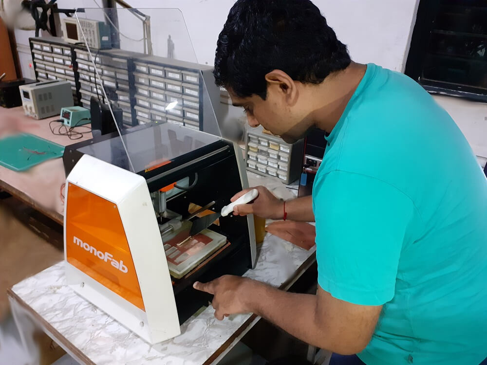
A. Operate PCB milling machine
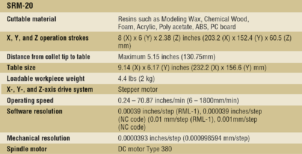
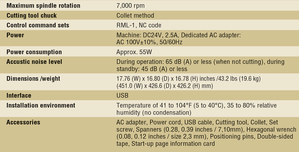
Roland SRM20 Milling machine is a precision three-axis machining, including PCBs down to 0.25 mm feature size, and machineable wax to make tooling for molding and casting. A wide range of materials, including modeling wax, chemical wood, foam, acrylic, poly acetate, ABS and PC board can be precision milled using the SRM-20 small milling machine, allowing you to create realistic 3D prototypes that are virtually identical to production parts. Engineered for optimum efficiency and productivity, the SRM-20 is a next-generation desktop mill that boasts a micro-step motor drive system for clean and precise contours and a phenomenal feed rate that is two times faster than previous generations.
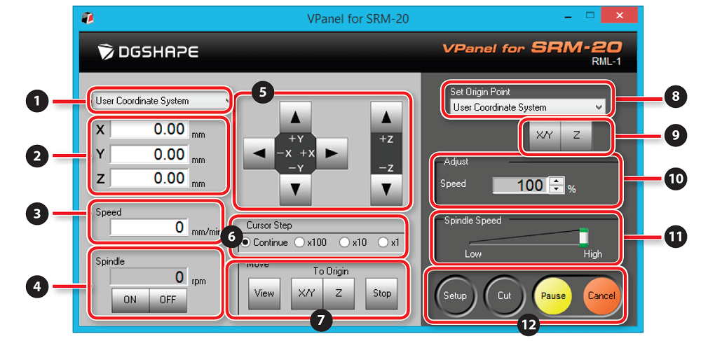
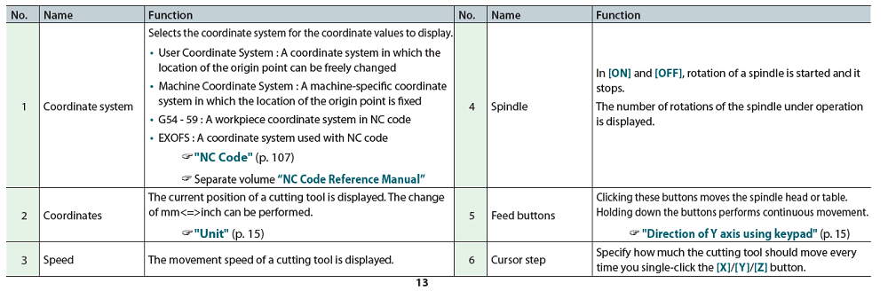
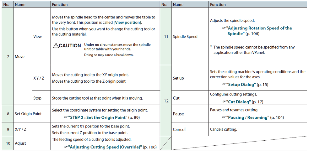
The SRM-20 has touch-button VPanel controller to regulate feed rate, spindle speed and milling on a complete X, Y, Z axes, and a new independent collet system that allows for faster setting of the Z-axis base point and quick tool changes. Click to know more
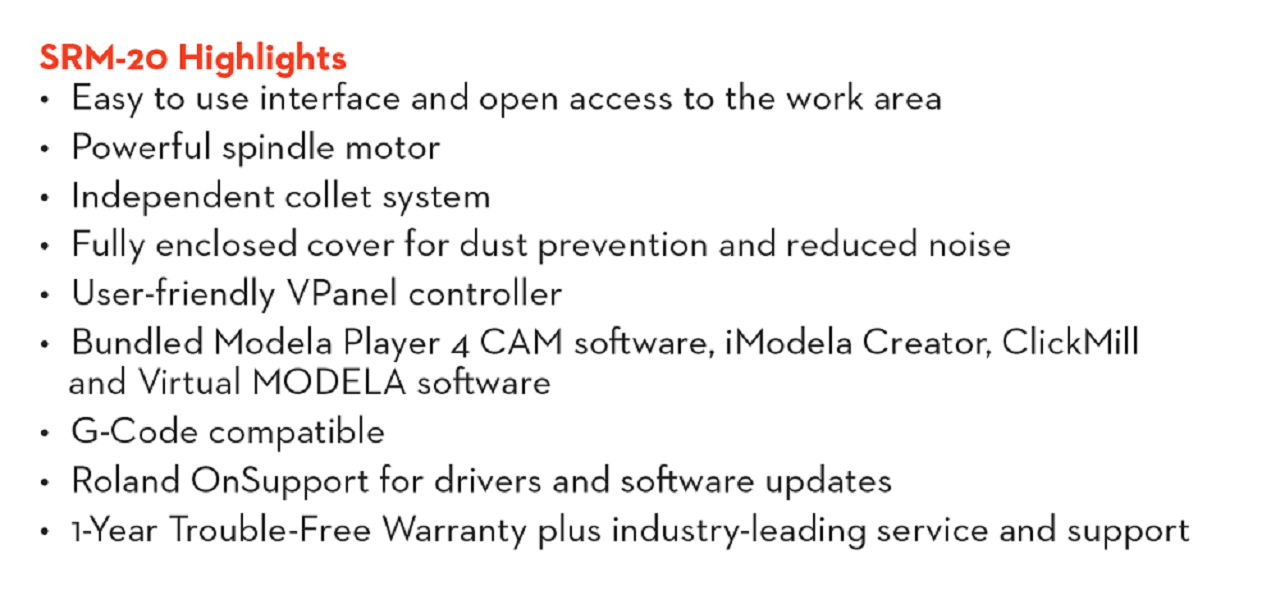
SRM-20 Highlights
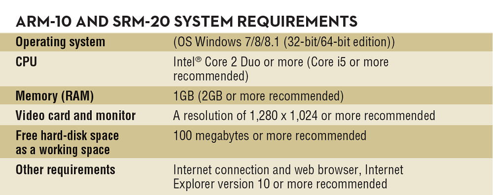
Specifications and system requirements of SRM-20
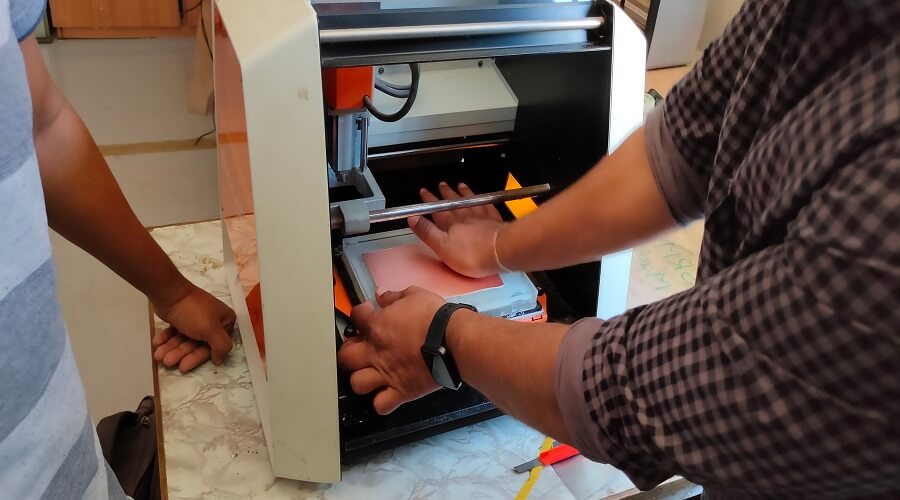
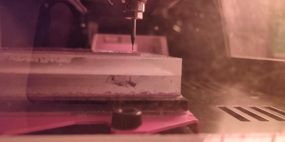
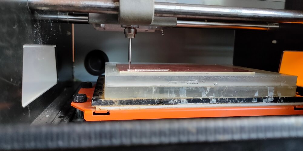
How I operated the PCB milling machine:
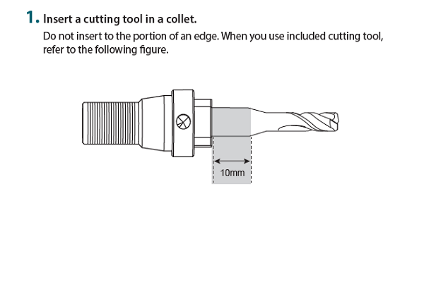
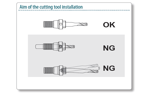
1. Setting up the cutting tool (End mill):
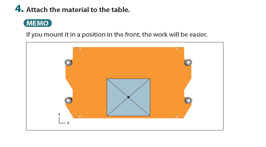
2. Setting up the substrate on the machine table:
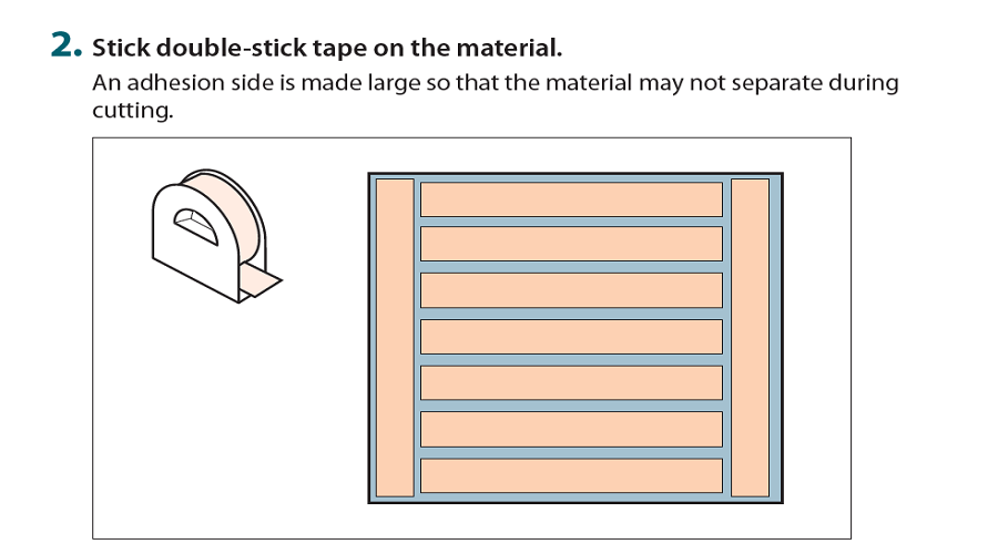
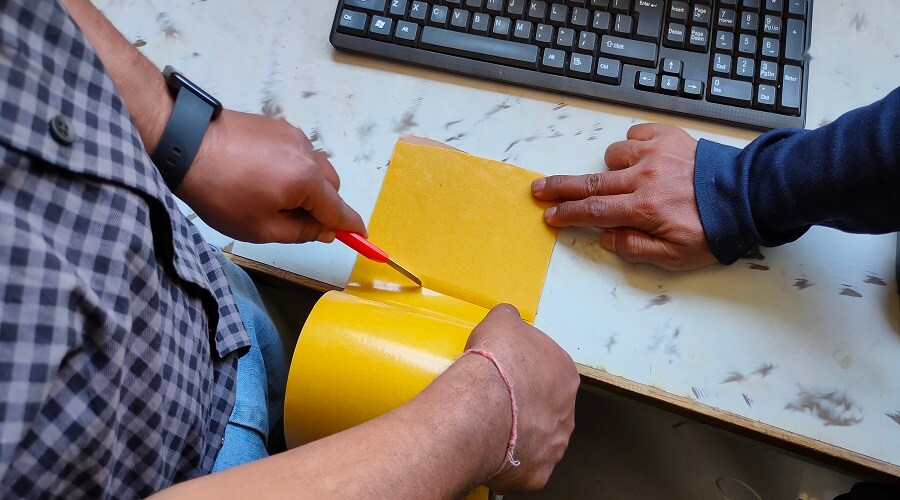
1. Put the double sided adhesive tape at the backside of the substrate surface. Make sure, it does not get bubbles and adhesive is applied uniformly. Cut the excess adhesive with cutter.
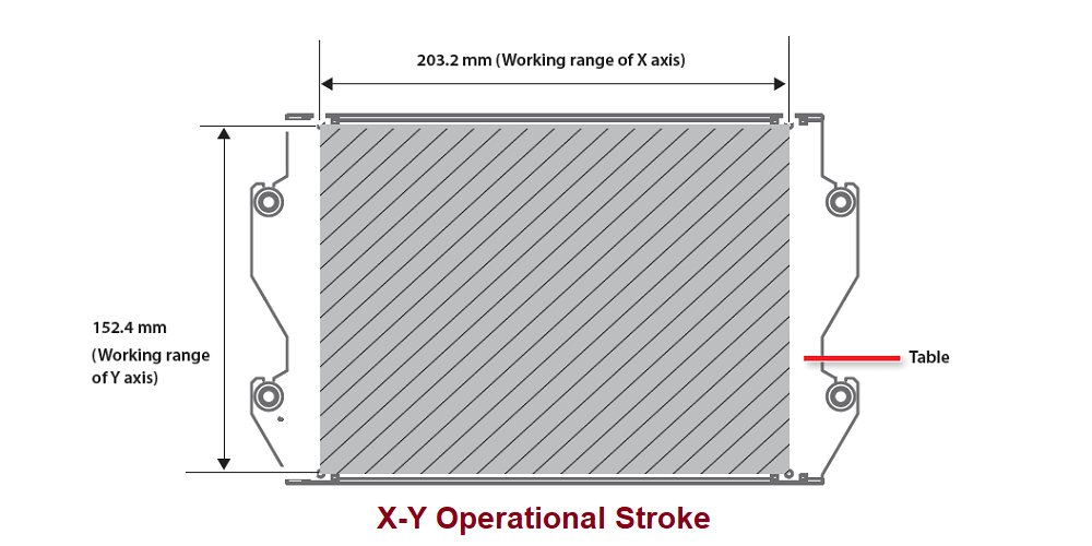
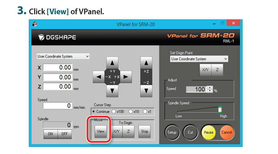
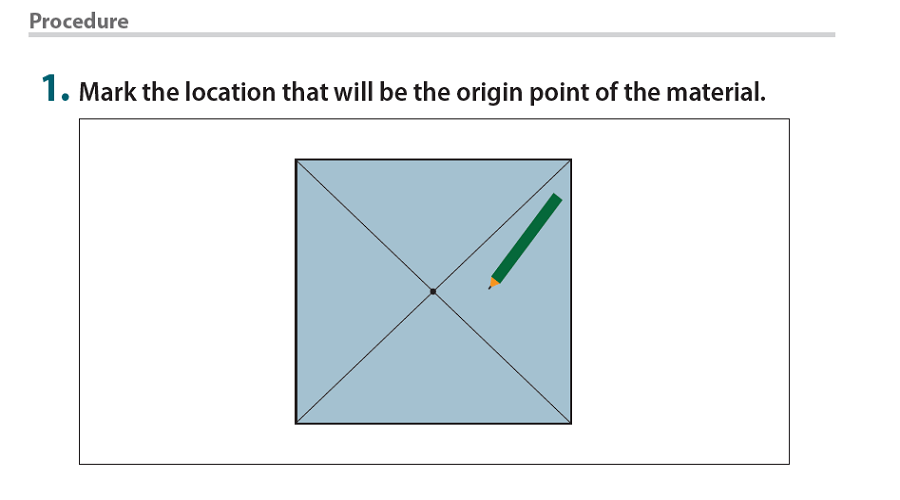
2. Place the substrate on the table We use the VPanel controller to move the machine table and bring it forward to be able to place the substrate properly in view mode. Set-up the substrate uniformly across the table in such a way that it has uniform level on the entire plane. Apply gentle pressure and check with spirit level. Then mark the Zero position on XY axis and mark it on the substrate with marker if possible to use the substrate properly without much of a wastage.
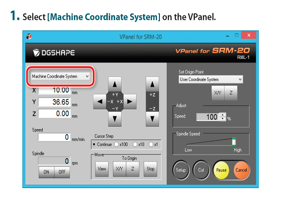
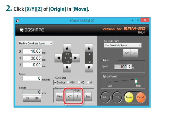
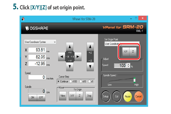
3. Prepare to set-up the origin point:
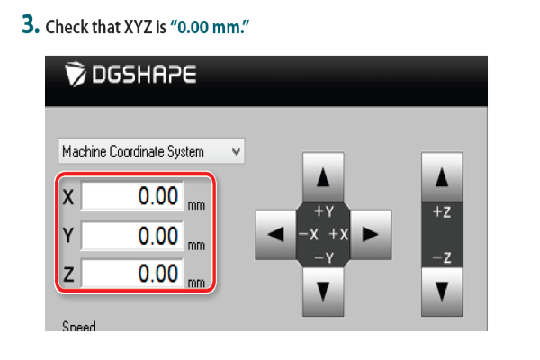
- First, Select [Machine Coordinate System] on the VPanel.
- Click [X/Y][Z] of [Origin] in [Move].
- Check that XYZ is 0.00 mm.
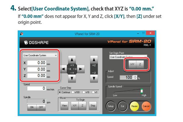
- Select[User Coordinate System], check that XYZ is 0.00 mm. If 0.00 mm does not appear for X, Y and Z, click [X/Y], then [Z] under set origin point.
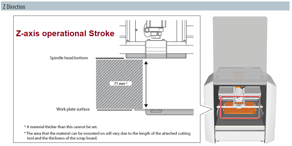
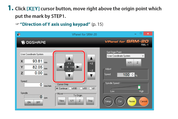
4. Set-up the origin point:
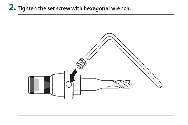
- Click the [- Z] cursor button to approximate the tip of the cutting surface of the material as much as possible. The hole of the mounting screw must be seen ( to loosen the set screw with the hexagonal wrench).
- Loosen the set screw, and then adjust the cutting tool so that its tip contacts the surface of the material.
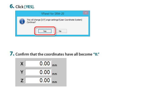
- Tighten the cutting tool in place again with the set screw.
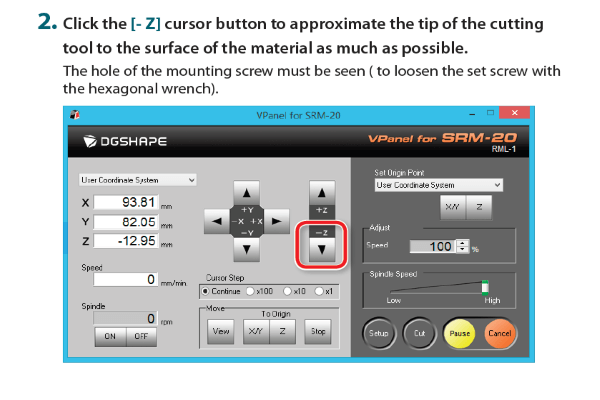
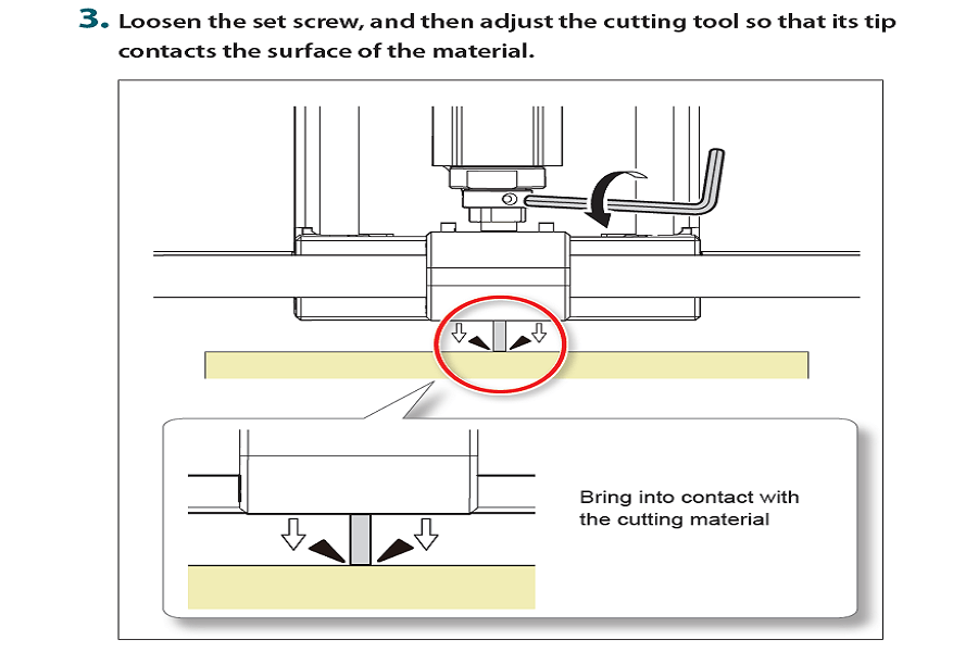
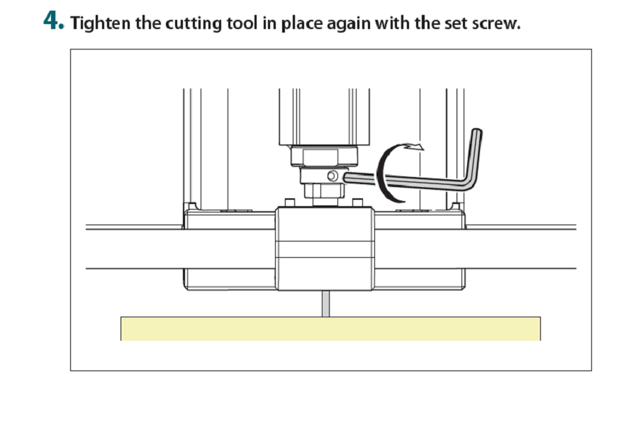
- Click [YES] and Confirm that the coordinates have all become 0.
5. Generate the tool path for tracing and cutting:
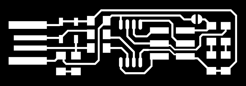

- Selected the trace PNG file first as shown in the picture below. I then set-up Zero for X, Y and Z absolute coordinate system.
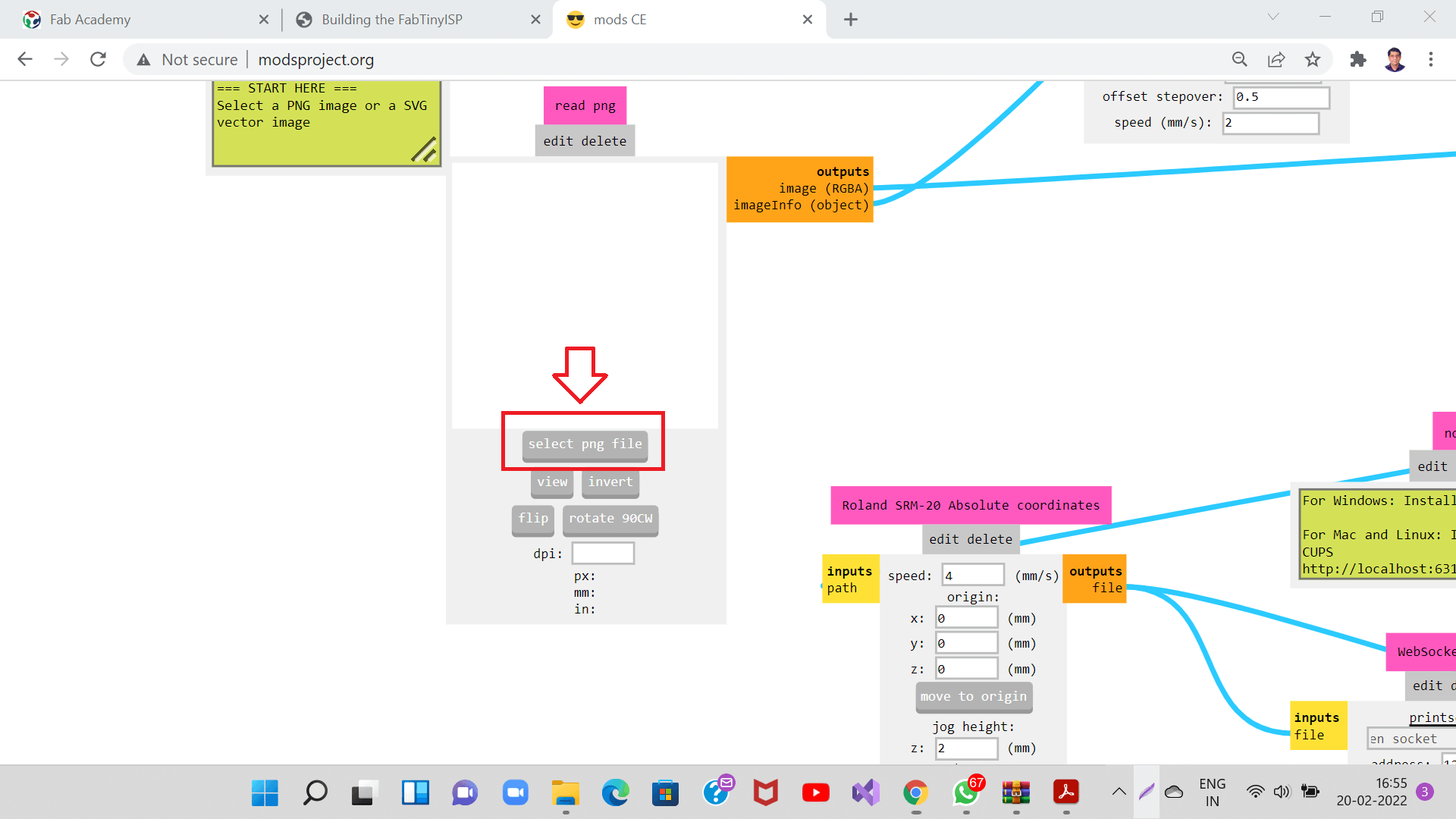
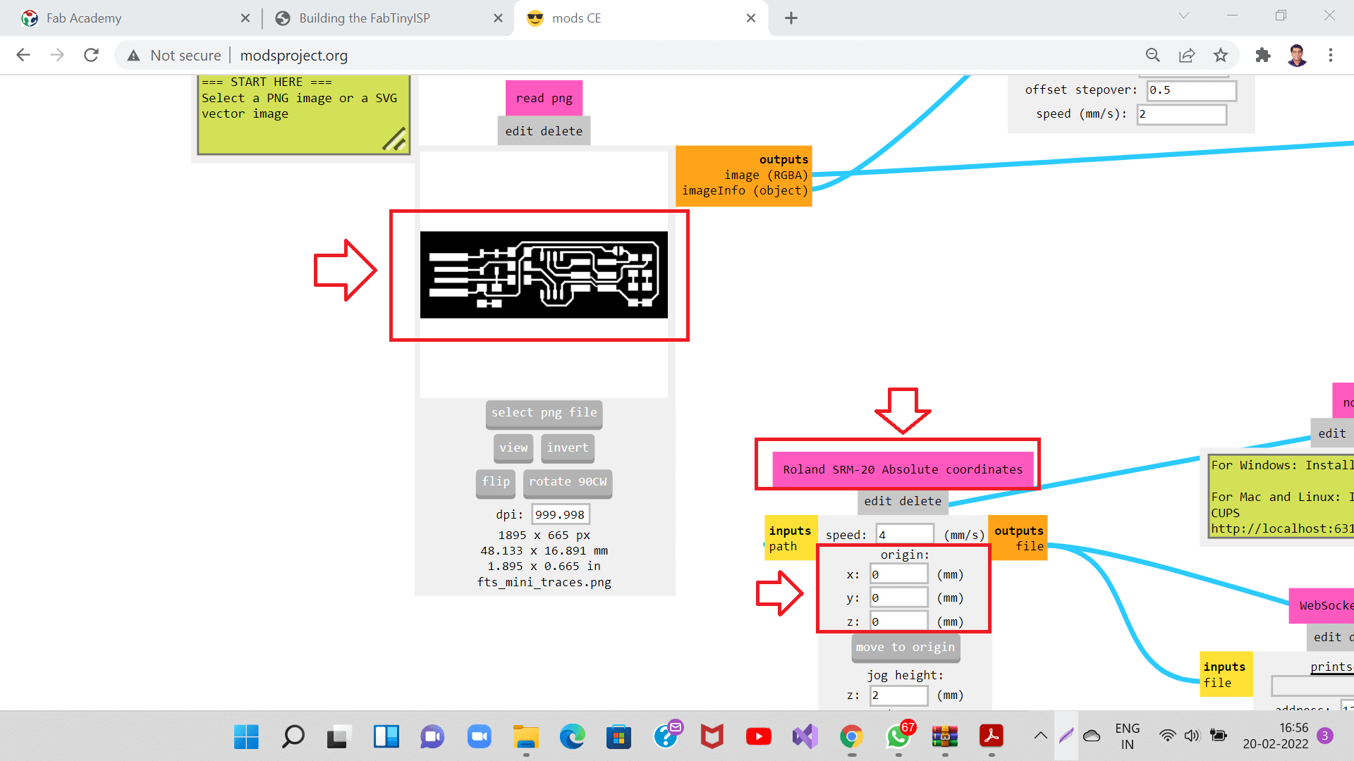
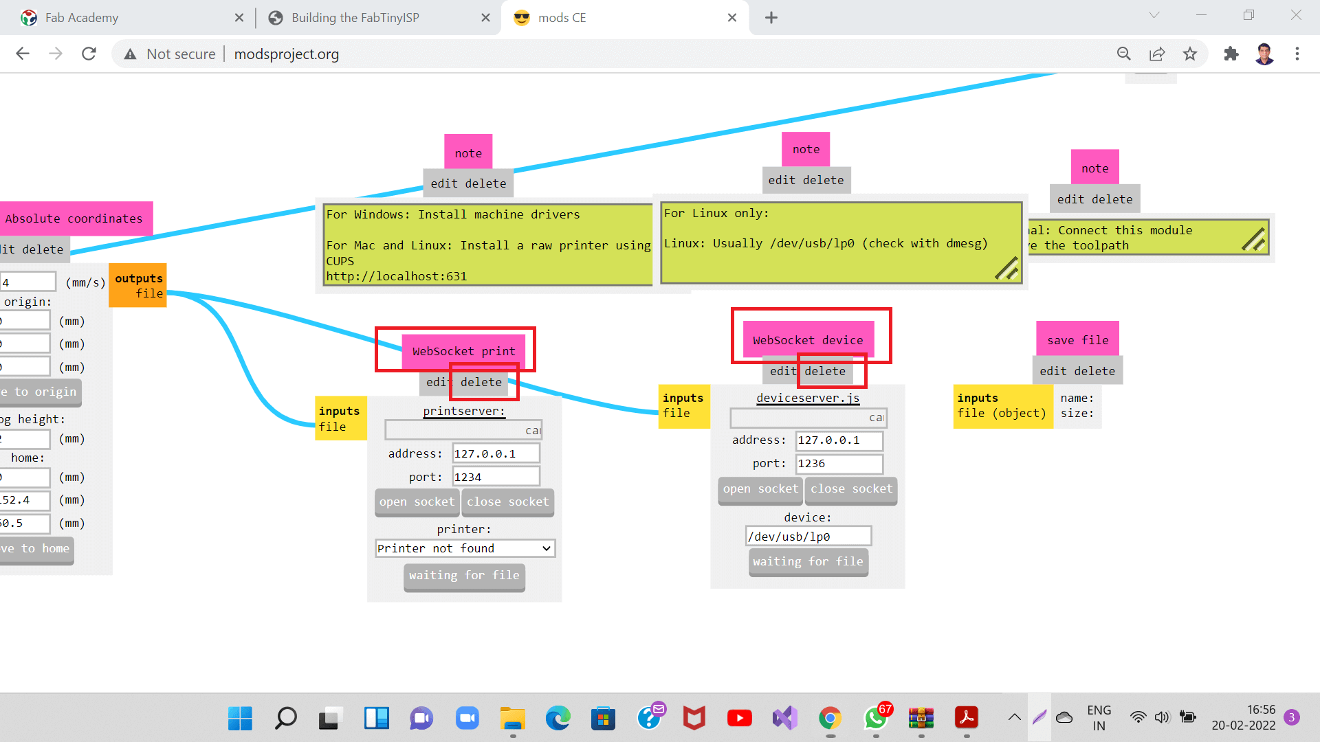
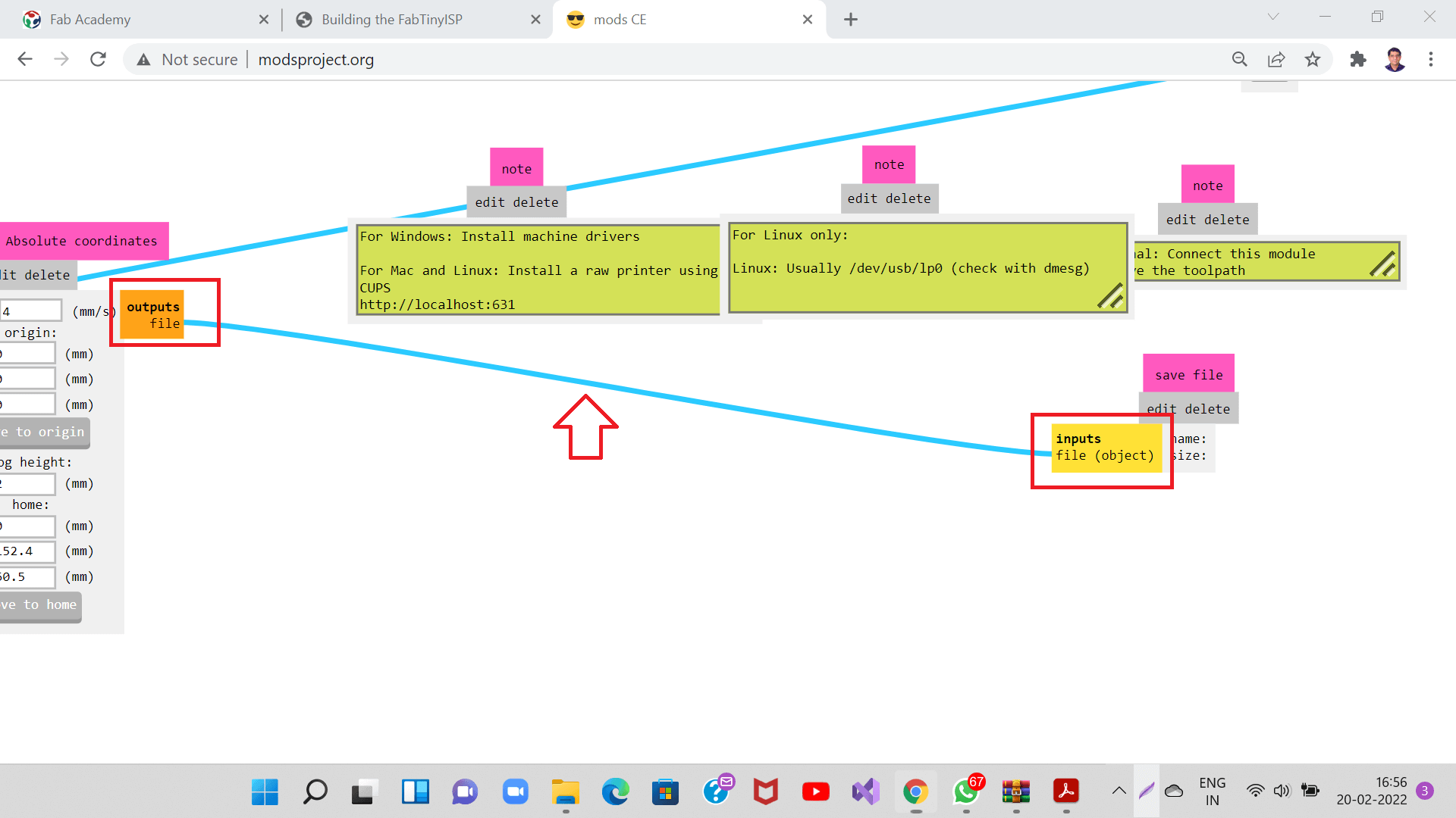
- I then connected output file of machine absolute coordinate to the 'save file button'.
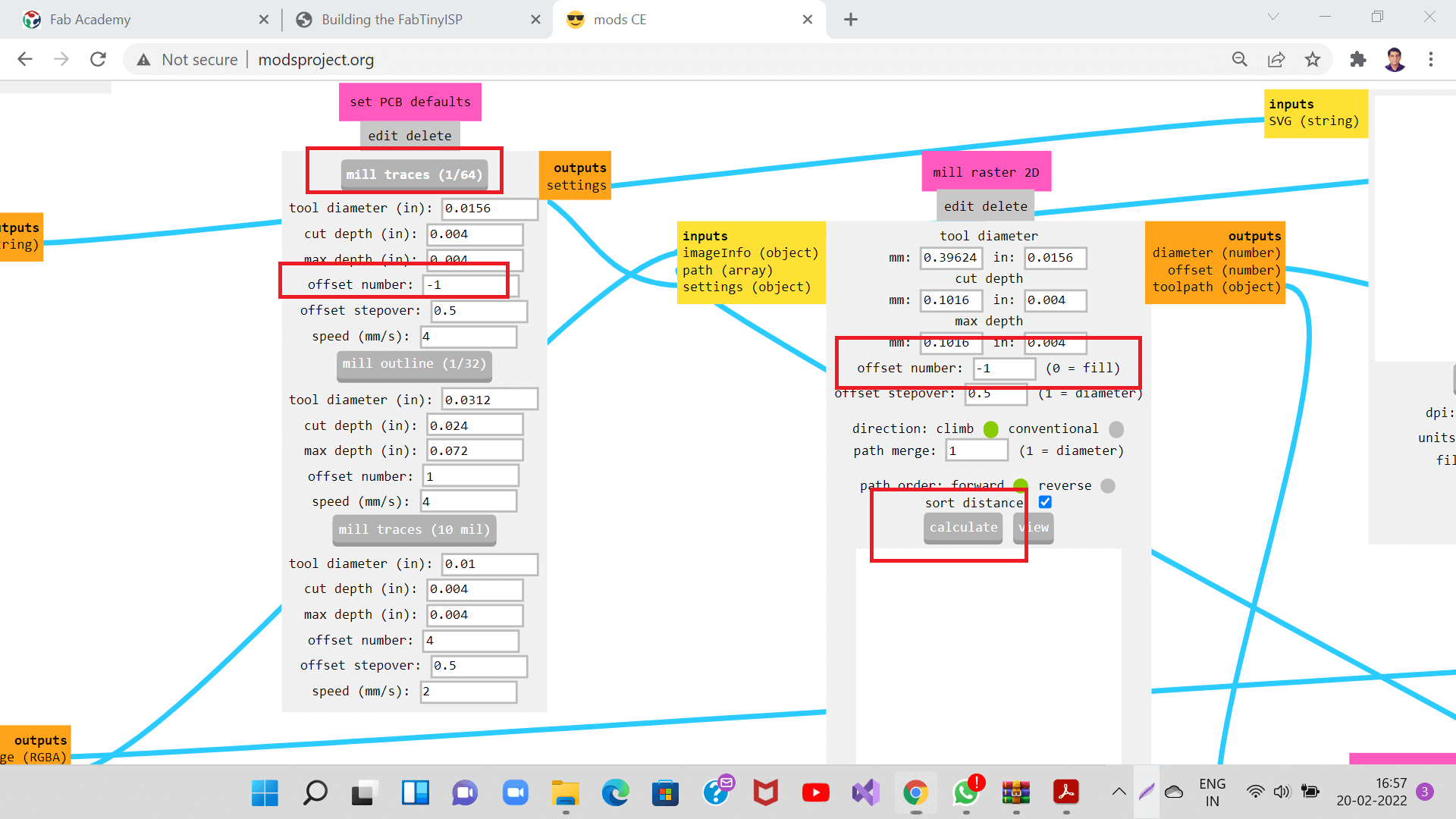
- I then clicked 'calculate' button under 'mill raster 2D'. Then tool path for tracing was generated and got downloaded automatically as shown in the picture below. I will use this tool path in VPanel controller to be sent to the milling machine to start tracing.
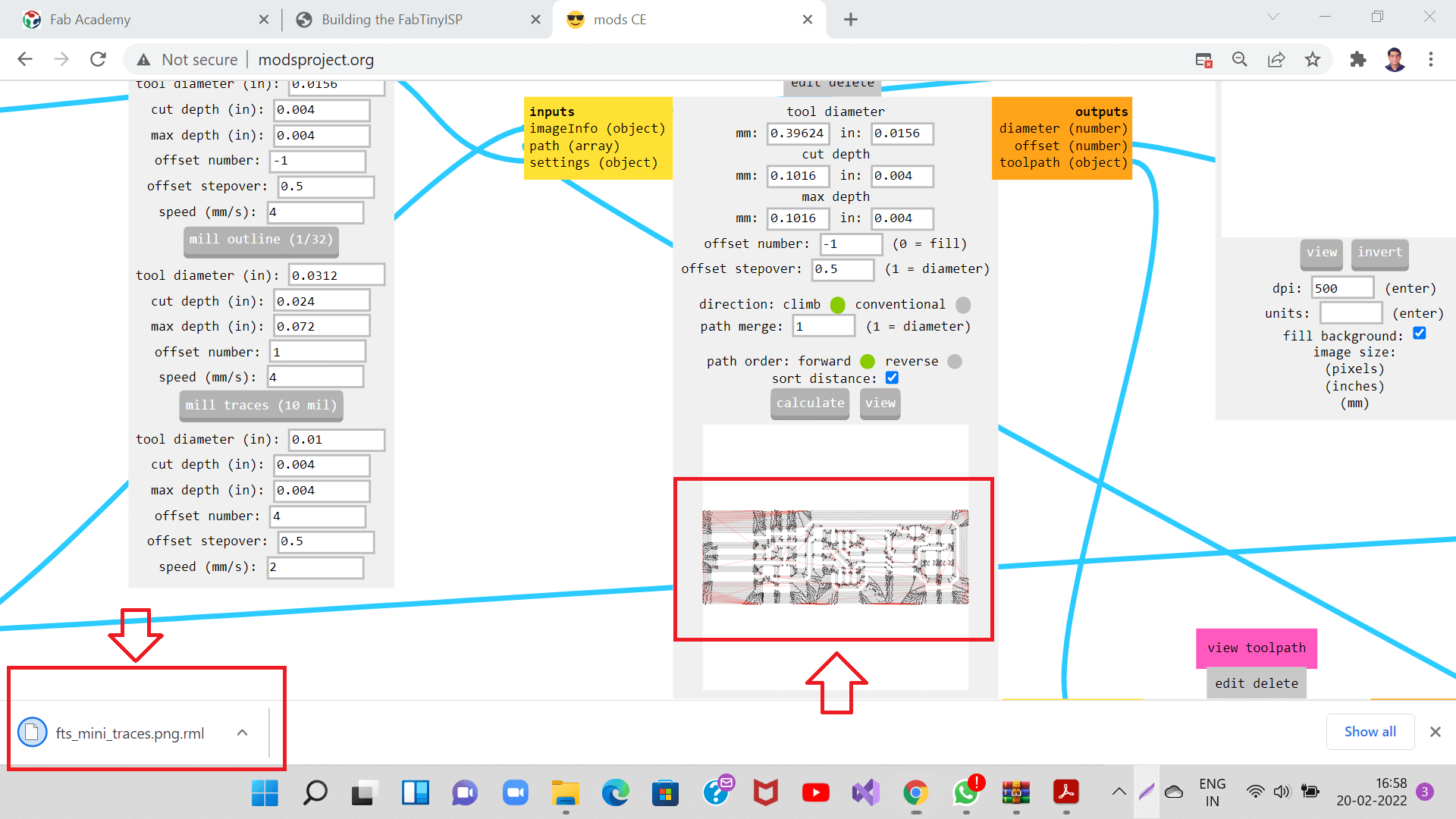
- I then deleted any previous paths and added new path. Selecting the newly added toolpath, I clicked on 'output' button to start the tracing operation inside the machine.
B. PCB assembly for in-circuit programmer
C. Checking my programmer
- Checked my board against the schematic and PCB layout image to make sure that I have installed the correct components in the correct locations and orientations.
- I inspected my board visually. Components needs be flat on the board, not tilted with pins in the air. Whether all the solder connections are smooth, and solder has flown both onto the pin and onto the pad. I also checked if there is a lot of exposed copper on the pad, or the solder is lumpy and has drawn up into a point where I removed the iron. This is where, I probably don't have a good connection. I needed to reflow by applying heat and flux (either from a flux or by adding a tiny bit more solder). Also I looked for unwanted solder bridges between nearby traces and pins.
- I used a multimeter to check for shorts between VCC and GND. I could not hear a sound that means, my connections were not short.D. Software installations
Before I could build and program the firmware onto my board, I needed to set up my development environment. I will be using this setup for all of my AVR programming for the class. The setup differs a bit for each platform, but once the software is installed it should work more or less the same on each platform.
1. Install Git: Since I am using Git on Windows, I have it already. If is not installed on your computer, click here to download and install Git for Windows. The defaults for all of the choices in the installer will work for our purposes.
2. Download the Microchip AVR Toolchain for Windows from microchip site and run the installer. When asked where to extract the files, click the "..." button and navigate to C:\Program Files, then click Extract. Click here to download the AVR toolchain.
3. Download GNU Make and launch the installer. Accept the default location for the installation. You can choose whether or not you want an icon in your start menu. Click here to download the GNU Make.
4. Install avrdude. Click here to download. Unzip the archive, and copy the archive inside to C:\Program Files.
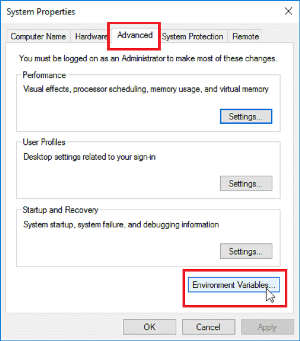
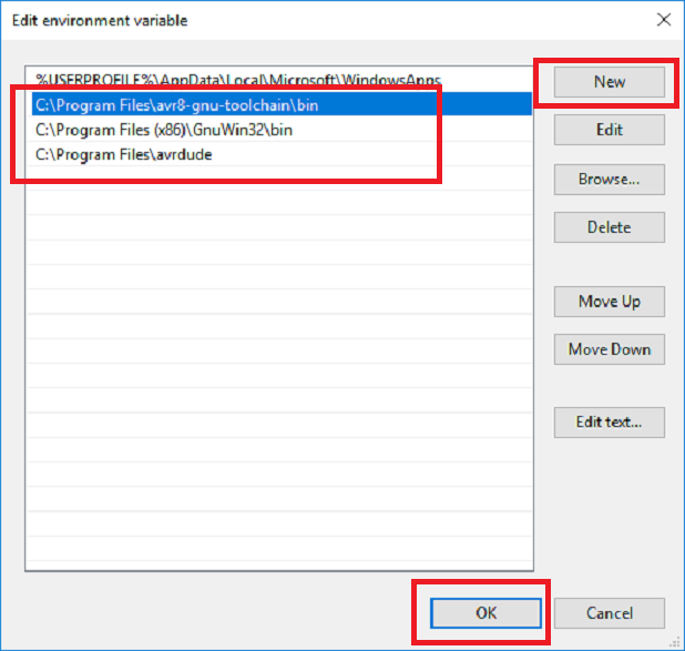
5. Update paths. Now we need to tell Windows where to locate all of the tools you've just installed when you type their names on the command line. Go to the Start menu and open the Control Panel, then go to System. From the left pane, choose "Advanced System Settings". Under the Advanced tab, click the "Environment Variables" button.
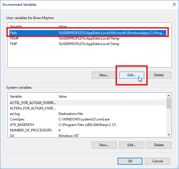
- C:\Program Files\avr8-gnu-toolchain\bin
- C:\Program Files (x86)\GnuWin32\bin
- C:\Program Files\avrdude
Click OK on all of the windows you've opened.
E. Sanity Check
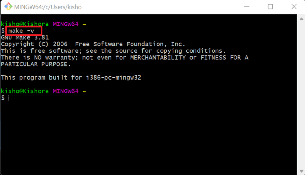
1. Make Type make -v in Git bash and press enter. You should see following message. If you get a "command not found" error instead, re-check your installation of make and your path variable setting for typos.
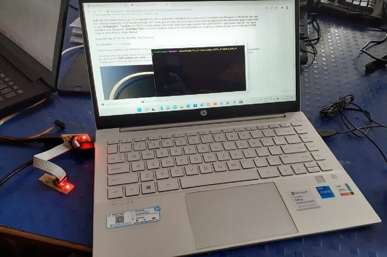
Now, you should be ready to go!F. Programming the programmer
- Small translucent blue programmer: avrisp2
- Large translucent blue programmer: jtag2isp
- White box with blue stripe: atmelice_isp
- Any fabbed board with an ATtiny on it: usbtiny
Edit the file called Makefile. It is important to use a text editor intended for programmers; programs like Notepad or WordPad can add formatting information that breaks the file. On Linux, gedit (GUI) or nano (command line) are good options; Windows users might want to use Notepad++. TextEdit on OS X usually works, just make sure you save as plain text and not RTF (and make sure no ".txt" gets added to the filename). Sublime Text is another popular choice on several platforms. In general whatever you use to edit your HTML code is probably an okay choice.
Near the top of the file, find the line that says: PROGRAMMER ?= usbtiny and change usbtiny to whatever programmer you're using.
- Connect the programmer to the ISP header on your board. Note that there are two different orientations in which you can connect the cable; it is imporatant that you get pin 1 in the right place. Pin 1 is marked in the board diagram with a dot and has the MISO signal connected to it. If you look at the plastic connector on the programmer cable, there should be a small arrow, dot, or manufacturer's name marking the corner with pin 1. Note that there's no enforced standard for which direction the cable comes out of the connector, so look for the pin 1 marker.
- that the programmer is connected correctly and pin 1 on the connector matches up to pin 1 on the board
- that your board is well-seated in the USB port
- that the ATtiny45 is installed in the correct orientation
- that your soldering looks okay on the ATtiny45 and ISP header (note that shorts can happen where the traces run underneath the connector)
If you've checked all of the above and still can't program your board, use a multimeter to verify that there is continuity between the pins on the chip and the ISP header, and that there isn't continuity where there shouldn't be (shorts between adjacent pins or traces).
- First, we'll set the fuses that control where the microcontroller gets its clock source from. (The USB requires the clock to come from the PLL, and not be divided by 8). This will allow us to check that the board works as a USB device, but it won't yet be able to program other boards.
- Only after confirming that USB works, we'll set the fuse that disables the reset pin and turns it into a regular GPIO pin. This will let the chip use the reset pin to program other boards, but will disable the ability for this chip to be programmed again. Because this is not easily reversible, we want to make sure that everything else works first!
Run the make fuses command. This will set up all of the fuses except the one that disables the reset pin. Again, you should see several progress bars from avrdude. If this step fails but the previous one worked, you likely have an intermittent connection somewhere.
For Windows: Windows lists USB devices in Device Manager (Start - Control Panel - System - Device Manager), though it doesn't always tell you what they are until the correct drivers are installed. USB devices may also appear in "Devices and Printers" or "Hardware and Sound". If you don't know your Windows machine well enough to find whether or not the USBtiny device is showing up, you might want to plug into someone's Linux machine or Mac to check for sure whether it's working.
- First, we need to change the bit that will turn the ATtiny45's reset pin into a GPIO pin. Once again, this will disable our ability to reprogram this ATtiny45 in the future, which is why we wanted to make sure everything was working before doing this.
Connect your ISP programmer to your board one more time, and run make rstdisbl in Git bash. This does the same thing as the make fuses command, but this time it's going to include that reset disable bit as well. You should see some progress bars, and with that, avrdude will never be able to talk to this chip again through the ISP header.
G. Test the Programmer
Assembly of other Programmers like UPDI, FTDI and JTAG
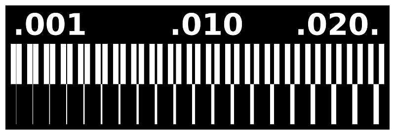
Using Vinyl Cutter for flexible PCB
Click here to go back to the top
What went well
In PCB assembly individual assignment- I was able to set-up the substrate and tooling very well. Machining of 3rd job was done very well. I did SMD soldering for the first time in my life. Initially I thought it would be very challenging. However, as I practised SMD soldering on some old boards, it gave me confidence to do soldering on actual PCB board that I had cut. The circuit connectivity check ran successfully using multi-meter. Programming of the board was also successful in the first attempt.
During other PCB fabrication (vinyl cutting)- After a few trial and errors, I learned to set-up cutting force and speed for flexible PCB cutting on vinyl machine. It was much better to cut and weed the flex circuit as compared to what I did for vinyl cutting during last week.What went wrong
In PCB assembly individual assignment- During milling of my first PCB, after setting up Zero coordinates on Z axis, I did not lift the tool. I started the tracing operation while the end mill was touching the substrate. I also believe, the tool was not inserted in to the collet properly. As a result, the tip of the end mill broke immediately and it spoiled the job.
During other PCB fabrication (vinyl cutting)- I could successfully cut the flexible PCB using the kapton tape on vinyl cutter. However, later realized that the programmer will be connected to the computer through the USB port and I will not be able to use this flex PCB board thtough USB. However, I am now confident to cut one flex PCB during electronic design week :)What I would do differently
- I could have used 60 deg cutting tool for flex PCB cutting on vinyl cutter. Since we did not have one, we ordered for next weekLearning Outcomes
- I can use MODS project to generate tool path for PCB milling
- I will confirm if the end mill is insterted and tightened properly in to the collet before starting the milling operation. I will also ensure to lift Z axis after setting zero coordinated and before starting the milling
- I can now do SMD soldering, it needs patience, hand-eye coordination. It is an art basically :)
- I learned how to use multimeter and its different settings
- I got a chance to learn what is dry solder
- Mistakes I did during vinyl cutting last time helped me to do better during flex PCB cutting on vinyl cutter this time
- I learned the importance of documenting my work in detail as it gives me an opportunity to go through the entire assignment, week's work as a whole once again