WEEK 06
ON THIS PAGE WE WILL FIND A BRIEF DESCRIPTION OF MY JOB THROUGHOUT THE SIXTH WEEK
GENERALITIES
This week the work consisted of creating an electronic board with a button and a led. This item also had to be programmed with Arduino for it to work. It is clear that once you make an electronic board with a microprocessor you need to program it to make it work. It can work in different ways thanks to programming, but since I'm new to the subject, I hope I can achieve my goals.
| Day | Wenesday | Thursday | Friday | Saturday | Sunday | Monday | Tuesday |
|---|---|---|---|---|---|---|---|
| 09:00 | |||||||
| 10:00 | Meeting CT | Assigments | Assigments | Local Review | |||
| 11:00 | Meeting CT | Assigments | Assigments | Local Review | |||
| 12:00 | Assigments | Assigments | |||||
| 13:00 | Assigments | Assigments | Regional Review | ||||
| 14:00 | Assigments | Assigments | Regional Review | ||||
| 15:00 | Fabacademy | Practice | Practice | write Documents | |||
| 16:00 | Fabacademy | Practice | Practice | write Documents | Review Documents | ||
| 17:00 | Fabacademy | Practice | Practice | Assigments | write Documents | Review Documents | |
| 18:00 | Fabacademy | Practice | Practice | Assigments | write Documents | Review Documents | |
| 19:00 | Practice | Practice | Assigments | write Documents | Review Documents | ||
| 20:00 | |||||||
| 21:00 | Tutorial | Tutorial | Assigments | write Documents | |||
| 22:00 | Tutorial | Tutorial | Assigments | write Documents | Write Documents | ||
| 23:00 | Tutorial | Tutorial | write Documents | Write Documents | |||
| 24:00 | Tutorial | Tutorial | write Documents | ||||
| 01:00 | |||||||
| 02:00 |
I was very afraid to remake my board with SMD components, SMT technology. I still understand little of this technology. I have to admit that although they are very small, everything is extremely cheap and they work wonderfully. If they are well made, they are more resistant as they are light in weight (in my case, in the fourth week, they fell to the ground 2 or 3 times without breaking).
Using software for design
For this job, I will be using Eagle software. Since I have never designed a board, it gives me more confidence to work with Autodesk software (I hope it has an environment similar to Autocad, so that learning is easier).
Eagle is electronic board design software that uses a CAD environment and libraries to help board designers create a printed circuit. The design is done in two environments. One where the schematics are built and another that is designed automatically where the components have to be placed. It is capable of auto drawing tracks, although we will try to do them without this help.
To learn how to handle this software, he used some tutorials that are on YouTube. If you want to access them, you can click here.
To use the software, I downloaded it from Autodesk Educational, where I have a university account.
To draw my electronic board, I used attiny44 as a starting point. Here I leave the links:
Once the software was installed, I started by creating a NEW PROJECT:
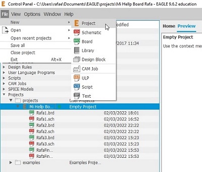
Once we have created the directory, the new project will have a gray light next to it. By double-clicking the left button, it will turn green, indicating that the files will be created in the created folder.
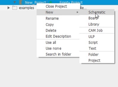
Another step is to create a scheme, for this we follow the following route:
Archivo>Nuevo>esquemático
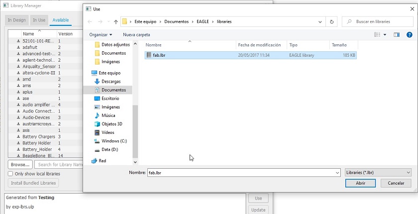
To be able to work with SMD components, it is good to install the Fabacademy library. Actually, Eagle has SMD components, but since we are new, it will take a long time to find them. We install the Fabacademy library, we will have it at hand and it will be easier for us to introduce the components.
We can download the library directly by clicking here.
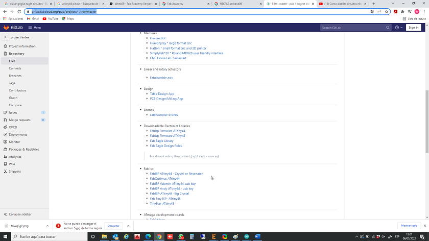 Appearance of the library in Gitlab
After having downloaded the library we will have to copy the .lbr file in the following path:
C:\users\.............\documentos\eagle\bibliotecas.
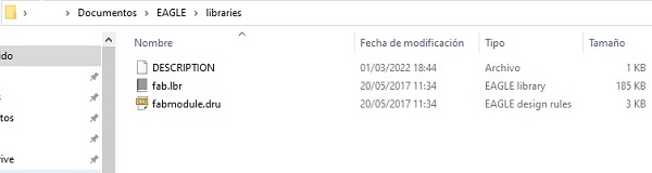 Image of the installation path
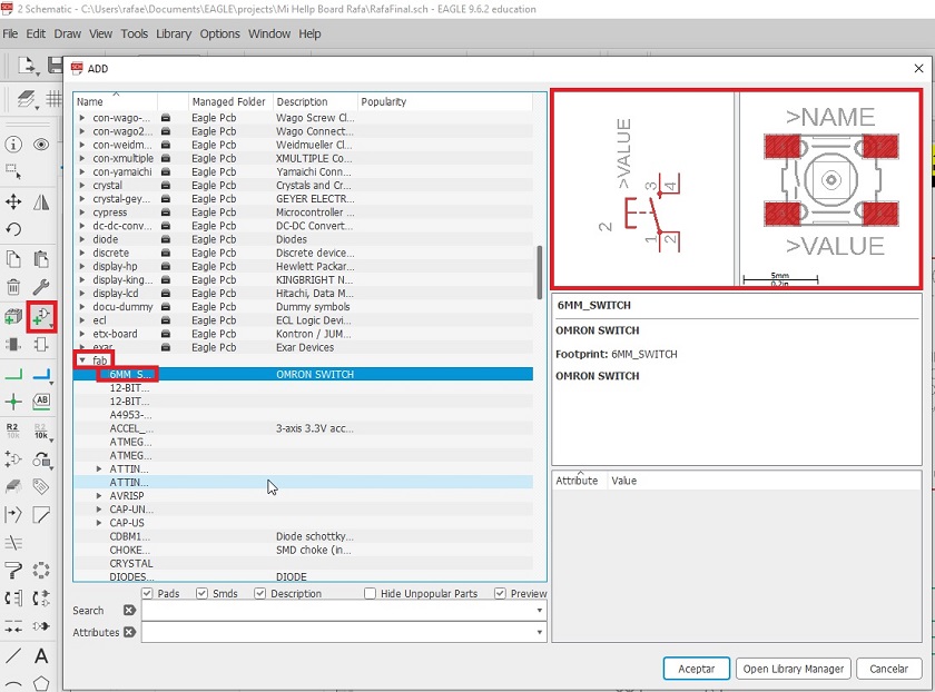
After having installed it, to make it work in the software, I have to go to the library manager and add them to the project.
 Adding the libraries
To add it, in the libraries tab, right click: Open library menu and search as in the image.
Once the library is loaded, I go to Add part and look for the components of my board:
 Finding my schematic components
As you can see in the previous image, in the part of the components on the left is the schematic and on the right the representation that will appear on the board.
Once I have entered all the components, I can connect them in two ways. Or I put a line that joins them or on the cross, right button and the names to which they are going to connect.
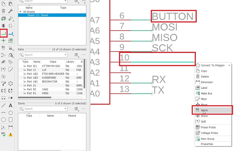 Connecting the components
Once I have entered all the elements, I will have the schema as follows:
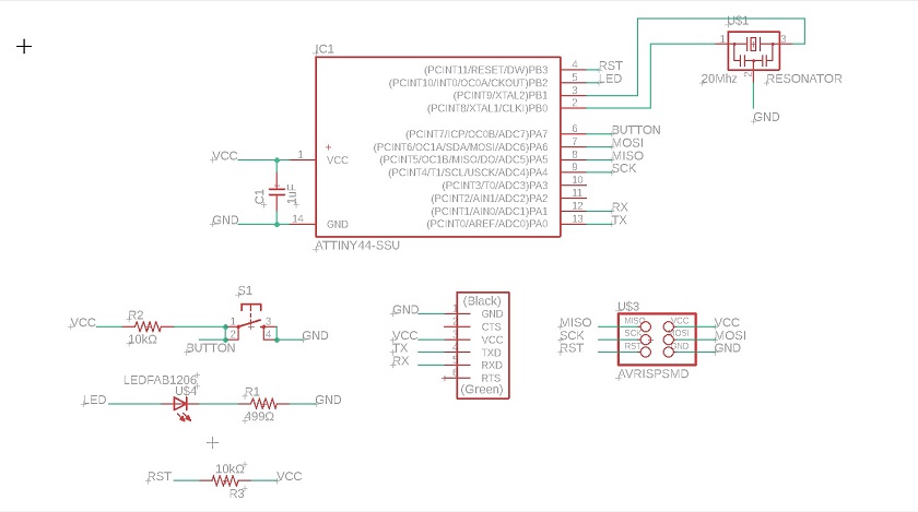 Finished scheme
Now I go to the second phase, I am going to generate the board, and I will have this image, where all the components are located in the lower left.
 starting to place elements on the plate
The window on the right represents the board, the plate, and the mixed components are located outside of it. Now it's time to move them so that the tracks can be drawn and all the components connected.
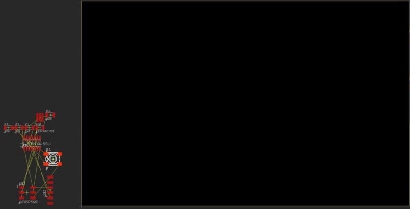
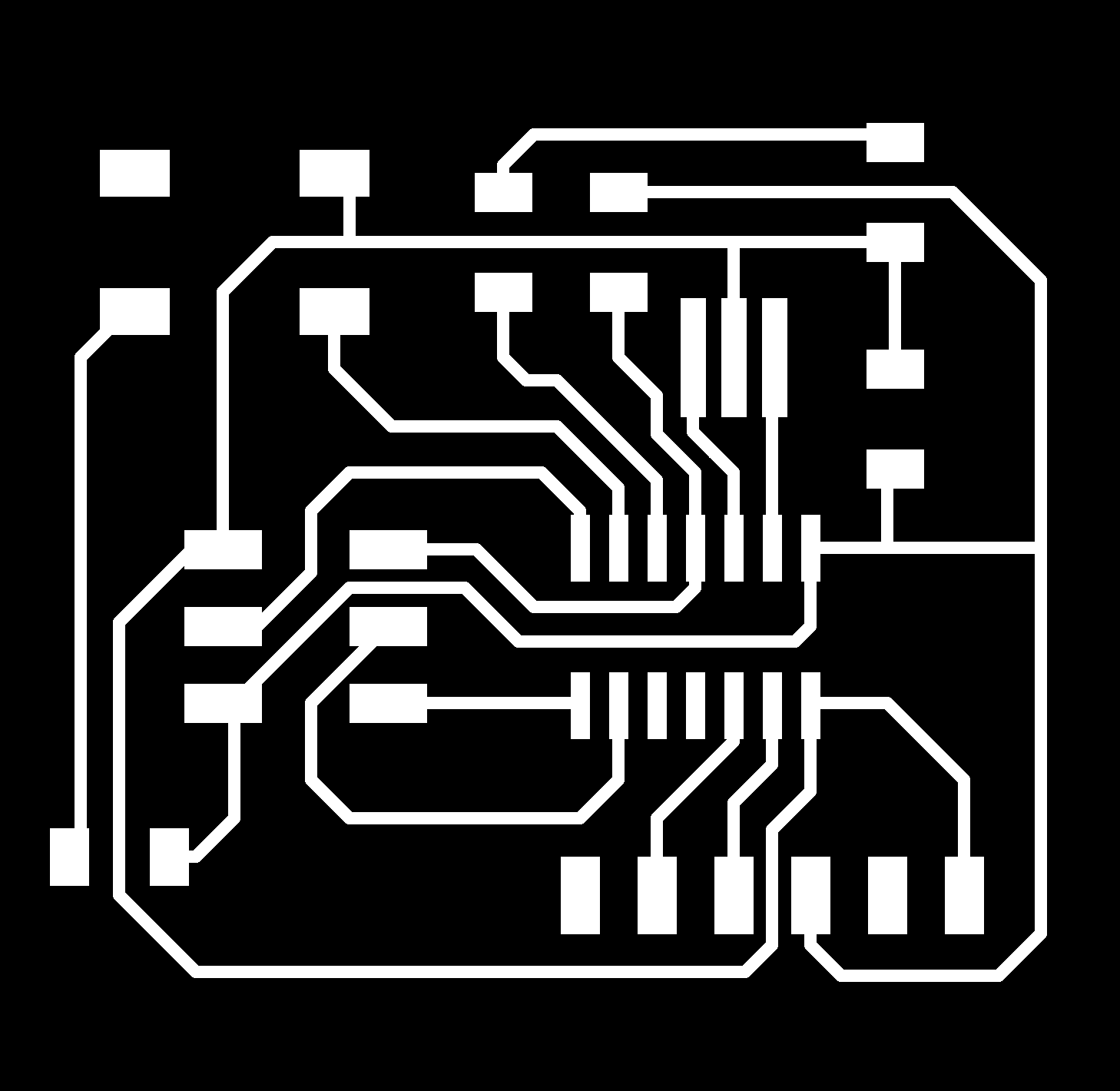
The generated design is very difficult to solve, there are many joints and after an hour of work, I have not solved anything. I could solve it using the autorouter, but my instructors tell me that you can't use it, you have to solve it by hand.
 Trying to have fewer line crossings
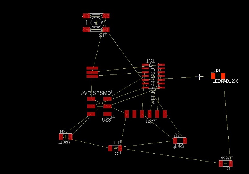
I start to not understand anything. So an idea occurs to me, I'm going to delete all the elements and leave only the connections, the ISP and the board. The solution allows me to see few lines and I can deal with them properly. Then I introduce all the elements and I modify the tracks to connect them all. In the end, the finished work looks like this:
 Scheme made by myself
I just need to connect a ground. Tomorrow, I will show it to my instructors.
I show it to them, and they tell me that it's not worth it, I'll have to start from the beginning.
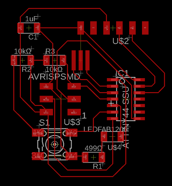
After a few hours of work and their help, I finished my circuit.
 Outline made with my instructors
The plate is very good, so we move on to production.
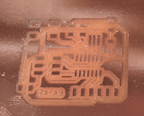 Milling error on the machine
The manufactured plate is very bad, all the tracks have been erased. It's a disaster. Hector Aparicio and Gustavo Salcedo, my instructors, explain to me that I have not properly parameterized the tracks, that I must put at least a value of 16 thousand in the Software so that they come out well. I'll have to re-draw and fabricate.
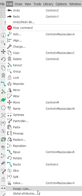 Changing line parameters
I go to the Dimension layer to modify the strokes, go to settings and load the FabAcademy parameters. I do this from the design rules window.
 Changing line parameters
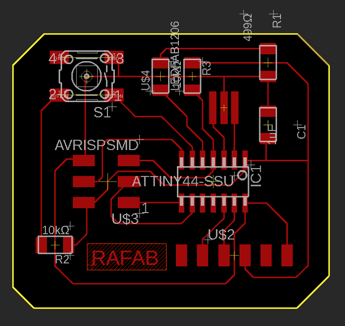
I redraw my Plate with the new rules:
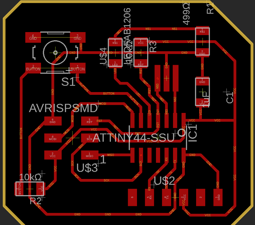 Finished scheme
Confirmed the unions, I create my image with the export command:
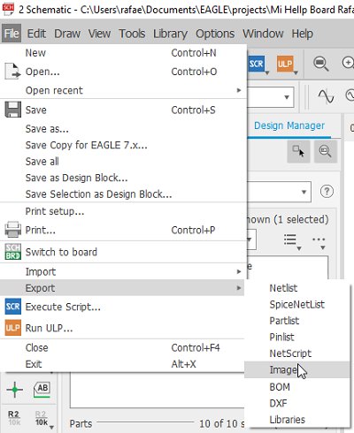 Exporting images
circuit milling
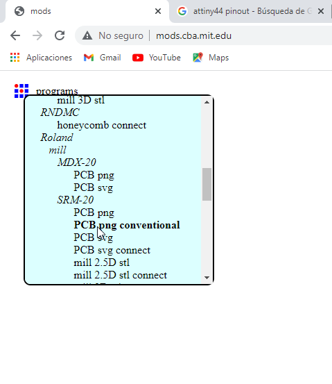
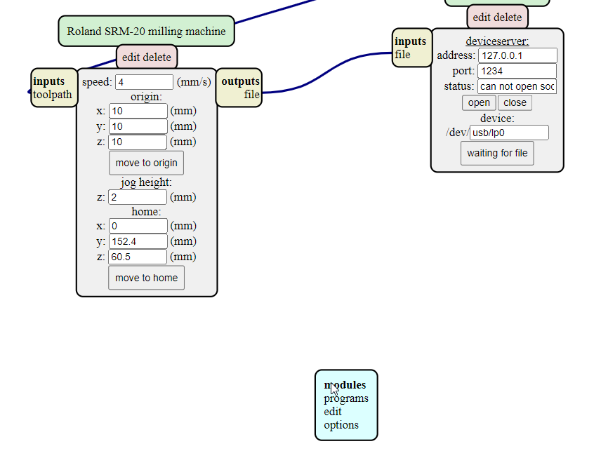
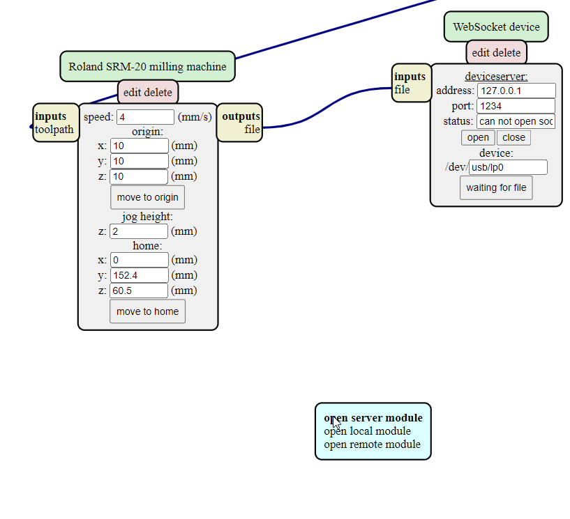
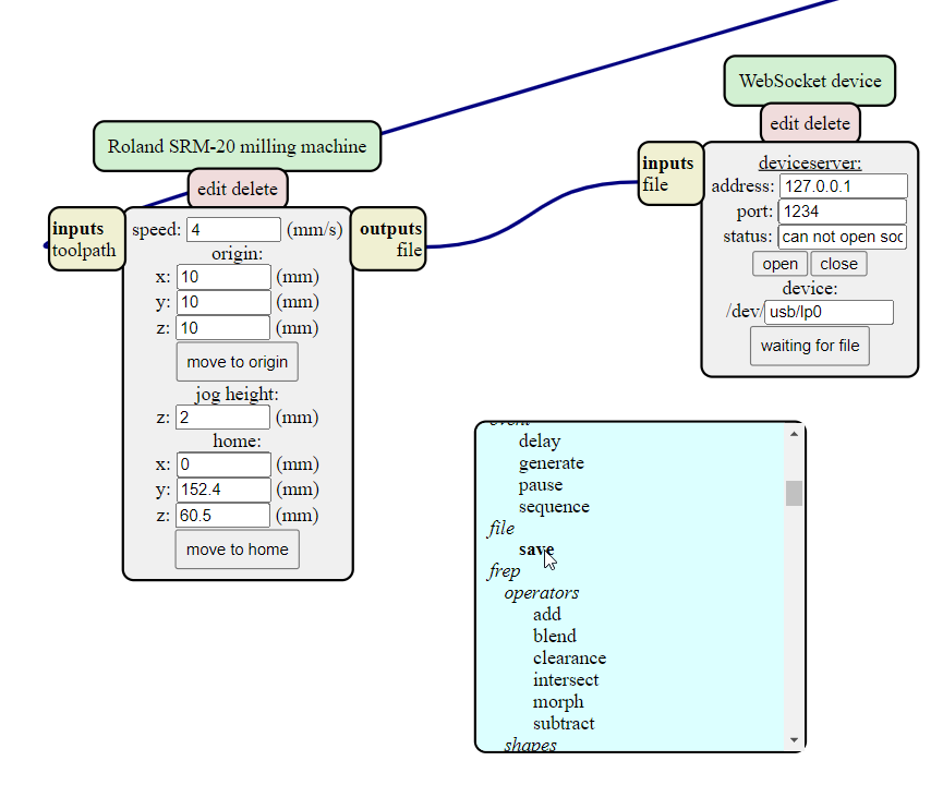
For circuit milling, I'm going to use the mods software as I used it in week four. Here I leave the link. I leave some screenshots for the steps to follow:
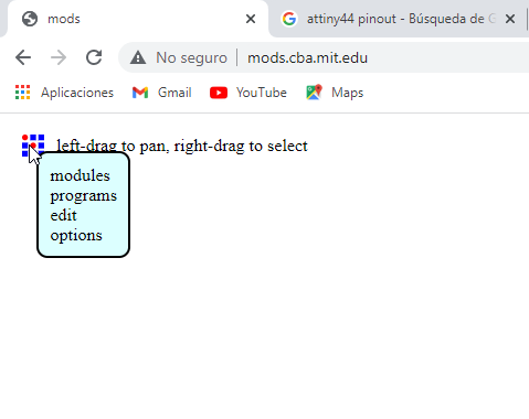 Step 1
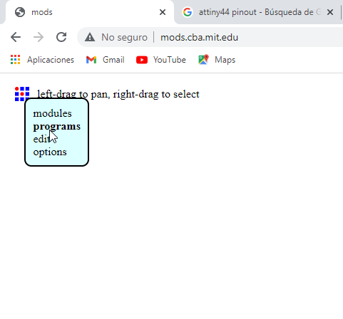 Step 2
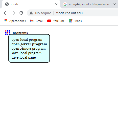 Step 3
 Step 4
 Step 5
 Step 6
 Step 7
After having prepared the program, we enter the images and mill the plate.
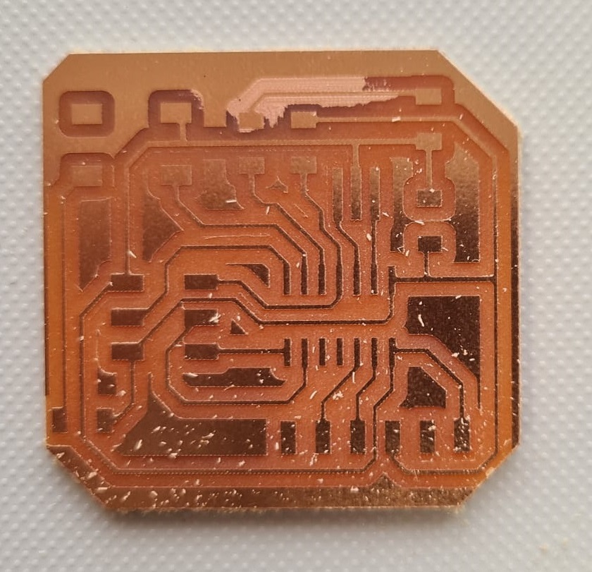 Finished milled electronic board
The finished board has some track failure, I am going to correct it with the cutter and I will solder the components.
Plate welding
To solder the components of the board, a tin soldering iron, fine tin filament, an electronic magnifying glass, tweezers to place the components and most importantly, soldering flux are used.
The components I use are the following:
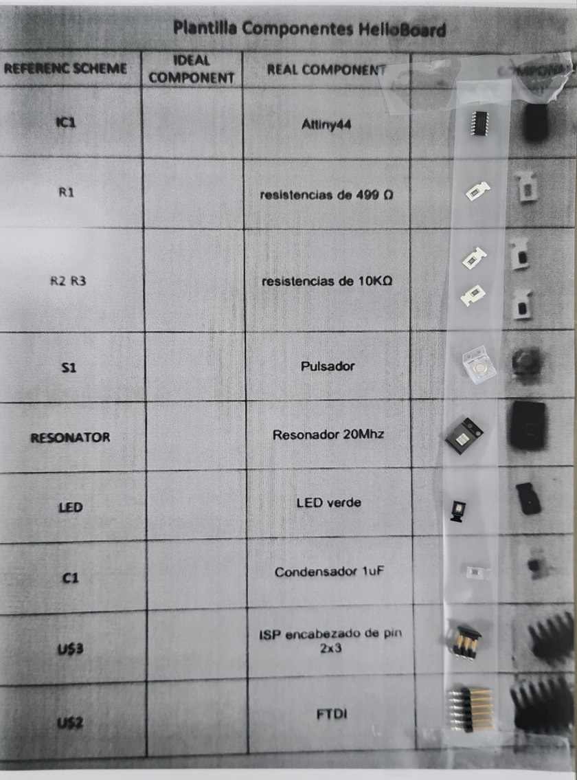 Components to be welded
When placing components, set the following priorities:
Microprocessor, icsp, led, resistors, capacitors, resonator, push button and finally the FTDI.
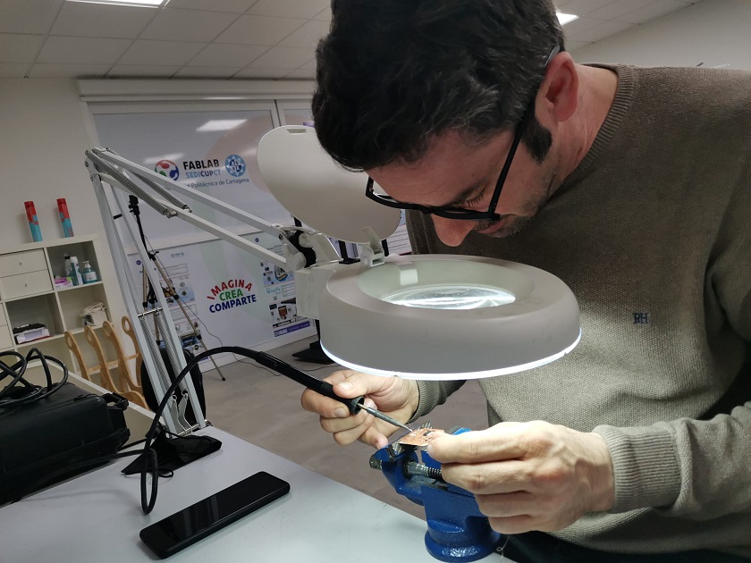 Me welding
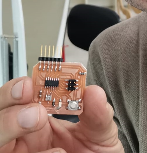 Finished
Finished plate, ready to program.
Software programming
For the programming of the board, I have used Arduino. Before using it you have to make some changes in the software.
 Uploading microchip firmware to Arduino
The first thing to add are the processor components. The Arduino is an open source program but intended for Arduino boards. To be able to use it with our cards, you have to add the components.
nother preliminary step is to find out if the microprocessor pins and the circuit outputs match.
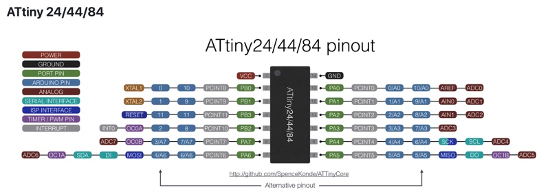 Checking the microprocessor pins
In our case, it is like this. We will not have any problem in programming.
 Verification of the installed microchip
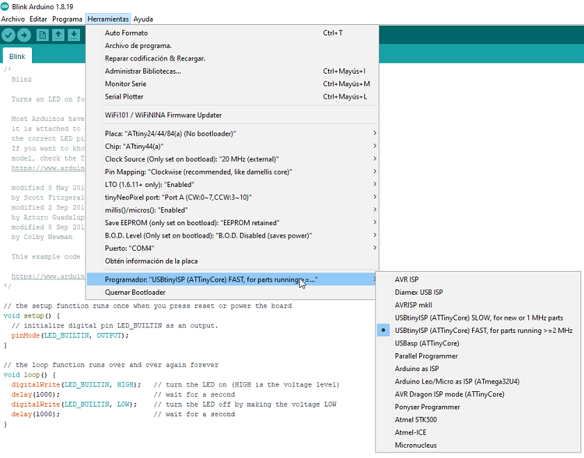
We check, whether it recognizes the port where the programmer is connected.
 Uploading the "Button" program to the board
We verify that the programmer is the right one.
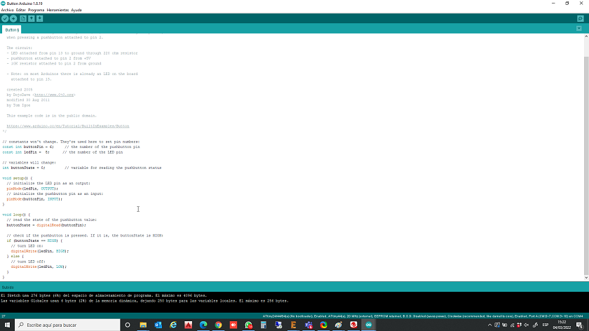
From the basic examples system we load the program for the button and burn it into the fabricated board.
Everything works properly.
CONCLUSIONS OF THE WEEK
It has been one more step to learn about the manufacture of electronic boards and their programming. Each time, it is more complicated but learning the basics is very enjoyable.
I was searching the internet for other programs about buttons and led lighting. There is a lot of material on the net and very well explained.
“What went wrong”: The milled plate. But I really enjoyed trying to fix it. Re-solder the components and test them. I really liked being able to fix it with the cutter and that in the end it worked.
It is a week where you can learn many things about boards and programming. Preparing the documentation wastes a lot of time and it's a shame. This week would give you more time to learn what to upload. It's a shame to leave it.
“What Went Right”: Eagle software is also made for newbies. It helps a lot.
"What will you do differently next time?": It would be interesting to add a theoretical week, on knowledge of microprocessors and programming.
MY FILES
Here I am uploading the files that I have been making this week


