6. Electronics Design
This week was Electronics Design, and it couldn’t happen at a worse time. CPCC was on spring break, which means that the two people with the most knowledge about this stuff were on vacation.
Again, I’m super grateful for Garrett taking the time to show me what he knows and help me get as far as I did.
A Quick Note
Before I jump into my second attempt, I just want to explain why I needed second board in the first place.
I had some trouble getting my board to light up. At first, I thought it was a programming issue. Considering it is easily my weakest point, that was naturally where I thought the problem was. After a lot of frustration and not a lot of progress, Garrett stepped in to help out. Between the two of us, we managed to get the board to light up (Huzzah!) but right when I grabbed my phone to take a picture, the light went out.
Odd.
By this point, David had shown up and he added his ideas into the troubleshooting hat, but we weren’t making much progress. We tried different program variables, different ports on the computer, different USB plugs, and finally, Garrett grabbed a wall mount and a simple USB cord and hooked up his programmer. The thought was that maybe something had happened to my programmer that was preventing my board from recieving the program. The LED on his board lit up, but it was very dim and unstable.
This should have been our first sign something was wrong, but nope.
Since nothing “seemed” wrong, David took my board and hooked it straight into the computer and POP!
Smoke, sparks, and a few heart palpatations later, my board was toast.
Turns out I had a short somewhere that was causing the problem, but it was subtle enough that it wasn’t noticeable until hooked up to a direct power source, one that wasn’t regulated to account for those sort of things. Thus, the light show.
Thanks David!
KiCAD
First things first, I have to design a board. I’ve never done this before, and I only have the bare minimum experience with electronics. So, for my first run, we’re gonna keep it simple. Especially since it’s Spring Break. It was up to poor Garrett to help me hobble along.
The board needs to do two things. It needs to blink and it needs a button to do a thing. Since I’m going to be using NeoPixels in my final project, I’m going to use that as my blinking light.
I’m using KiCad 6.0. When I first opened it, it brought up a menu with all the different types of editors and options available.
First thing after opening, I created a new project and gave it a name.
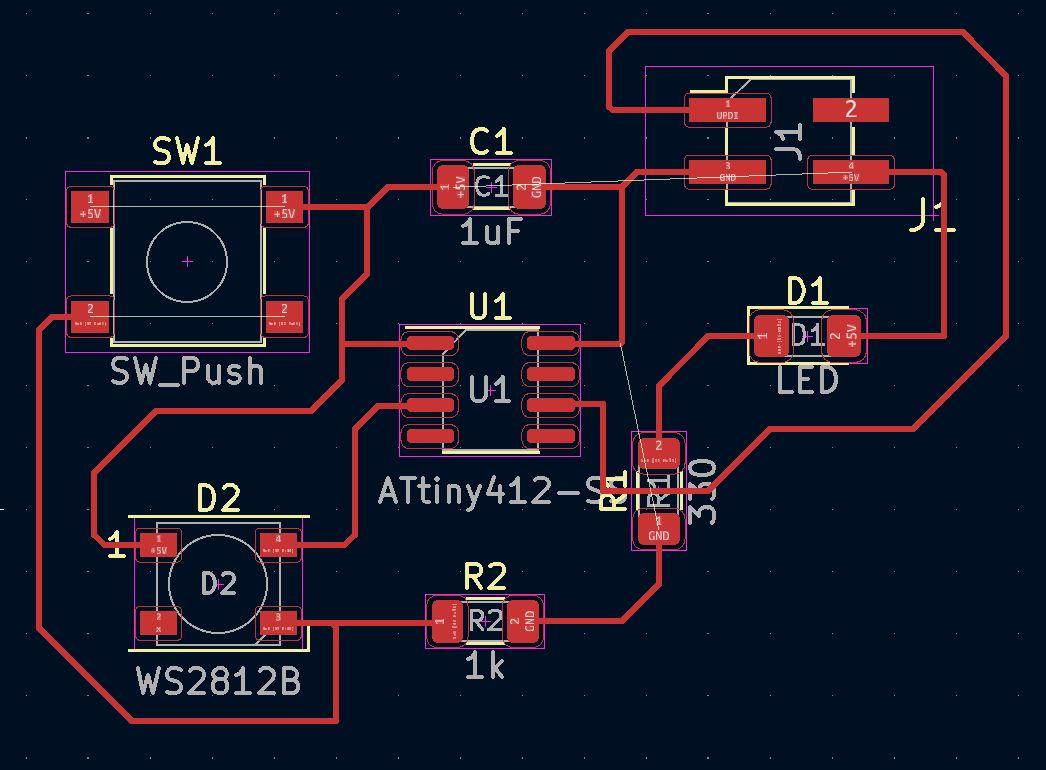
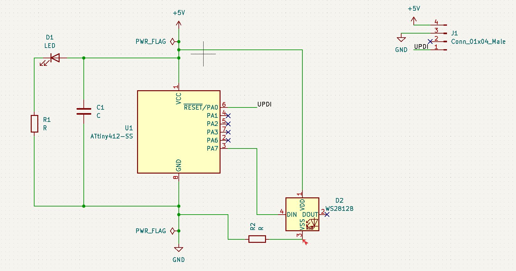
Schematic
From there, I opened up the schematic. This is where I’ll add all the components I need on my board. A new window will open with the schematic, which looks like a piece of paper with dots all over. Now we need to pick our components.
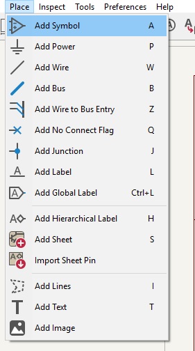
Under the menu option “Place”, then go to “Add Symbol”
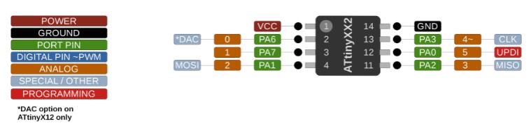
Garrett suggested working from the inside out, or with the chip we’re using then adding components from there. I’m using an ATTiny412, so I typed “ATTiny” in the search bar of the pop-up menu. There are a ton of options, so it’s important to know exactly which chip you’re working with.
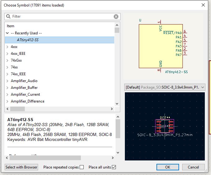
I really liked how clicking on the chip brought up a preview, both for the schematic and the PCB board.
I clicked okay and it closed the menu, and I placed the chip just somewhere in the middle. Where isn’t terribly important since we can move everything around later. Then it was just a matter of getting all the components I needed together.
One hint: If you highlight a component and hit “R” on the keyboard, it rotates the part 90 degrees. This is super helpful later when you’re trying to arrange the traces.
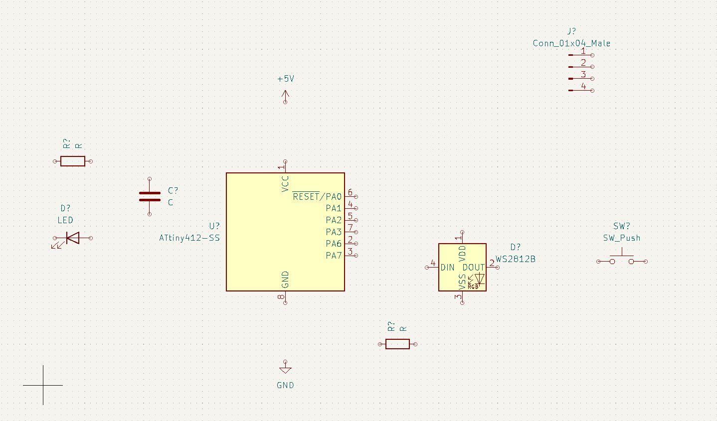
It looks messy, because it is, but that’s okay. I find it easier to arrange things when I have them all in front of me. This is going to look a lot like the first attempt, but hopefully arranged more neatly.
I also added my power and ground. These are located under the same menu, Place, but then I went under “Add Power”. I searched for 5v and Ground (I just went with the first generic option).
Now I need to connect everything. This is done with wires. Again under “Place”, click on “Add Wires”. After using it for a little bit, it’s just easier to use the keyboard shortcut, W.
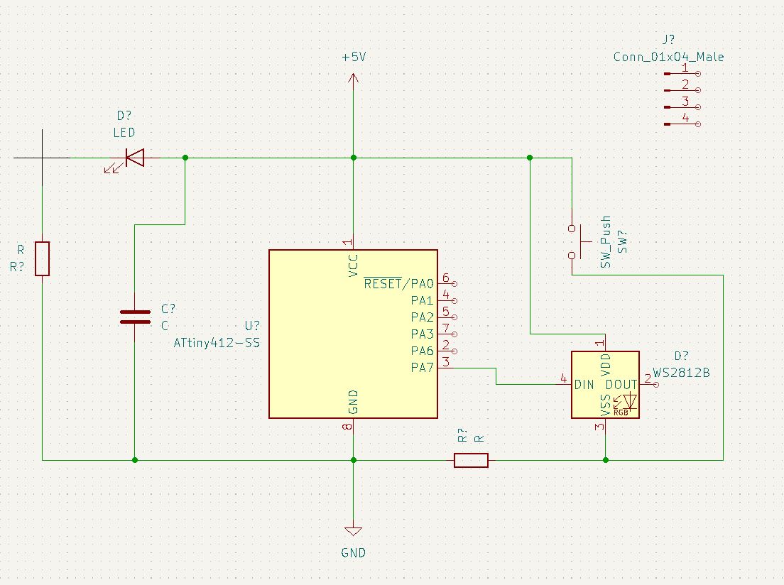
Almost done, but now I need to add the headers in. This can be done without having to stretch wires across the other connections.
Since the headers are separate, we have to add some of the same components as before for it to reference.
For power and ground, I added the symbols to the corresponding pins. Then I added a label for the UPDI, or the wire that will get information from the programmer and the chip. Labels are found under “Place”, and then “Add Labels”. The last pin isn’t going to be used, so I marked it with a “No Connect Flag”, also in the “Place” menu. I added a corresponding label to the pin on the chip.
Now everything has to get a label. In the row of symbols across the top, select the one that looks like R?? -> R42.
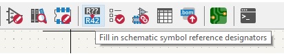
I didn’t change any of the options, just left it at default, and clicked “Annotate”. All the components are then populated with their own unique label.
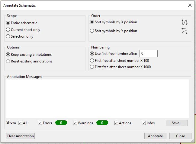
Now we need to run the Electrical Rules Checker. This does exactly what it says. It makes sure that all the connections are correct, that things aren’t left hanging, and that everything is labeled.
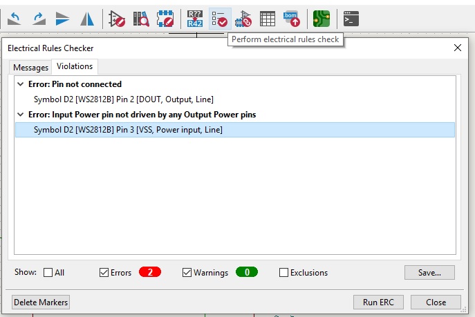
After running it, I have a couple things to correct, but this was better than I expected. Last time, we were basically chasing errors. Every time one was fixed, two would pop up.
These are easy to fix. The nice thing about this is when you click on a particular error, it will highlight where the problem is in the schematic.
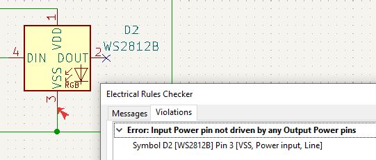
This is where it gets annoying. I double checked my connection here, and it is correct, so I’m going to leave it for now.
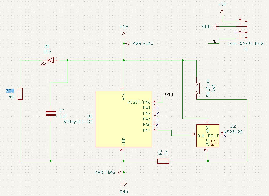
This was my first attempt on my own. It looks a lot like the first one, but I’m glad I retained a lot of what Garrett taught me, at least thus far.
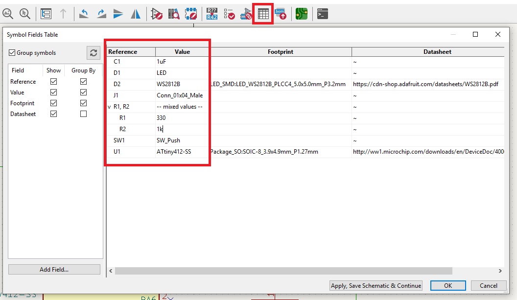
I almost forgot, I need to tell it what values I need for each part!! Back at the top, I clicked on the icon that looks like a table, and filled in the missing information under the “Values” column. When I finished, I clicked “Apply, Save Schematic & Continue”. Then hit “Okay”. It’s important to select apply first, or it won’t change anything.
NOW we should be ready to go.
Nope. One more thing. I tried to populate the PCB, but nothing showed up. After a quick review of my notes, I realized I forgot to add the footprints of the components.
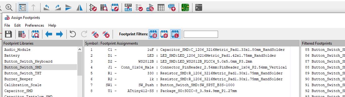
This one gets confusing really quickly because there are sooooo many options. The one consistent thing is the size of the parts, which is 1206. This is the same for the LED, the capacitor, and the resistors.
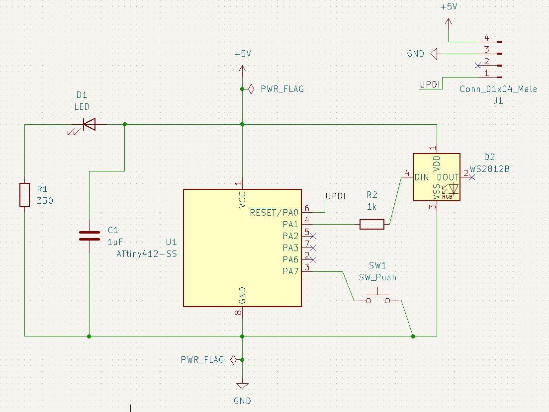
Thanks to a wild Adam sighting, my schematic is actually correct.
Adam came by the lab while I was working on this second version and noted that my button was wired incorrectly. Since I was basing this off my first attempt, I didn’t have a reference because we had added the button later. That’s probably why my first board ended up the way it did, but we’ll get to that. Anyway, now I had a signed off schematic to use and I could start working on the trace game.
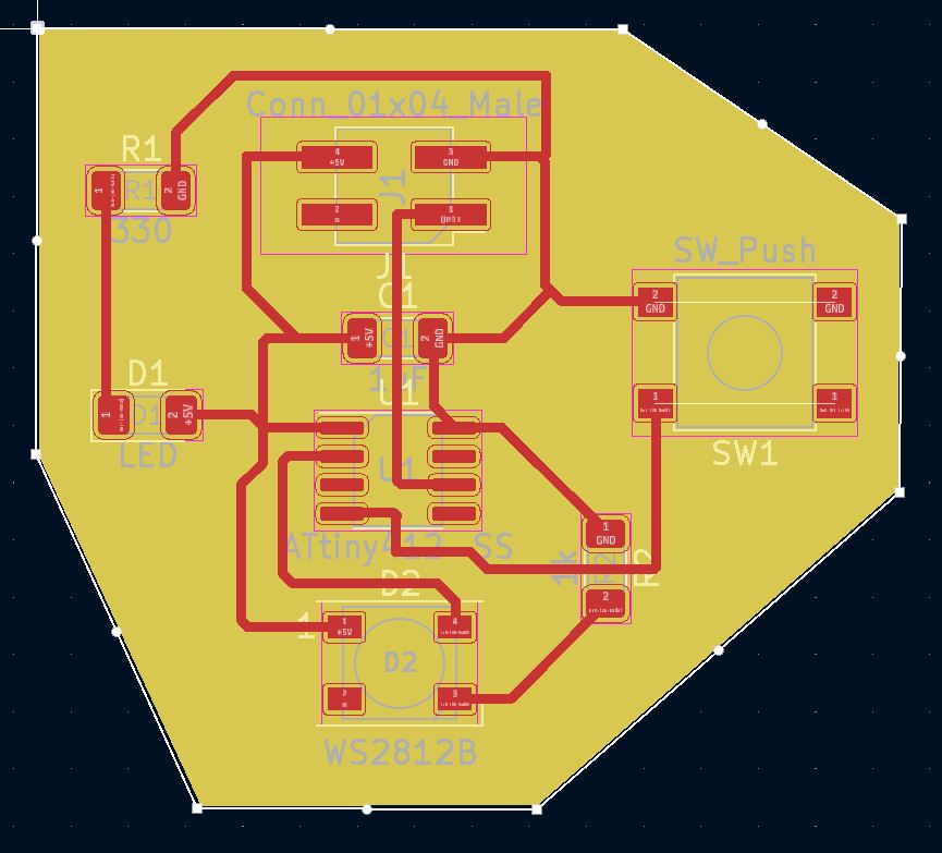
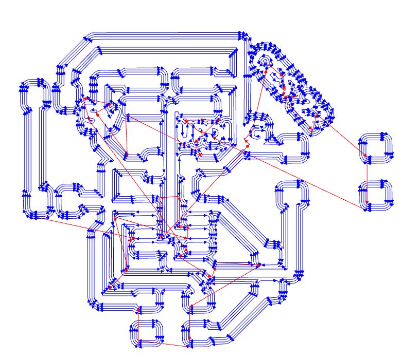
Traces
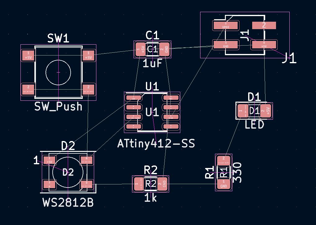
Now we have to sort this mess out again.
I’m not good at this game. There’s always something that I need to connect that I can’t quite make.
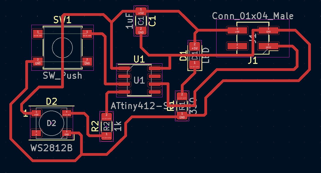
This took waaaayyyy longer than it should, and even after looking at it, I can already see better ways to arrange it. But I’m done! I’m not touching it any more.
Almost ready. Doesn’t look too bad. It’s better than the last one.
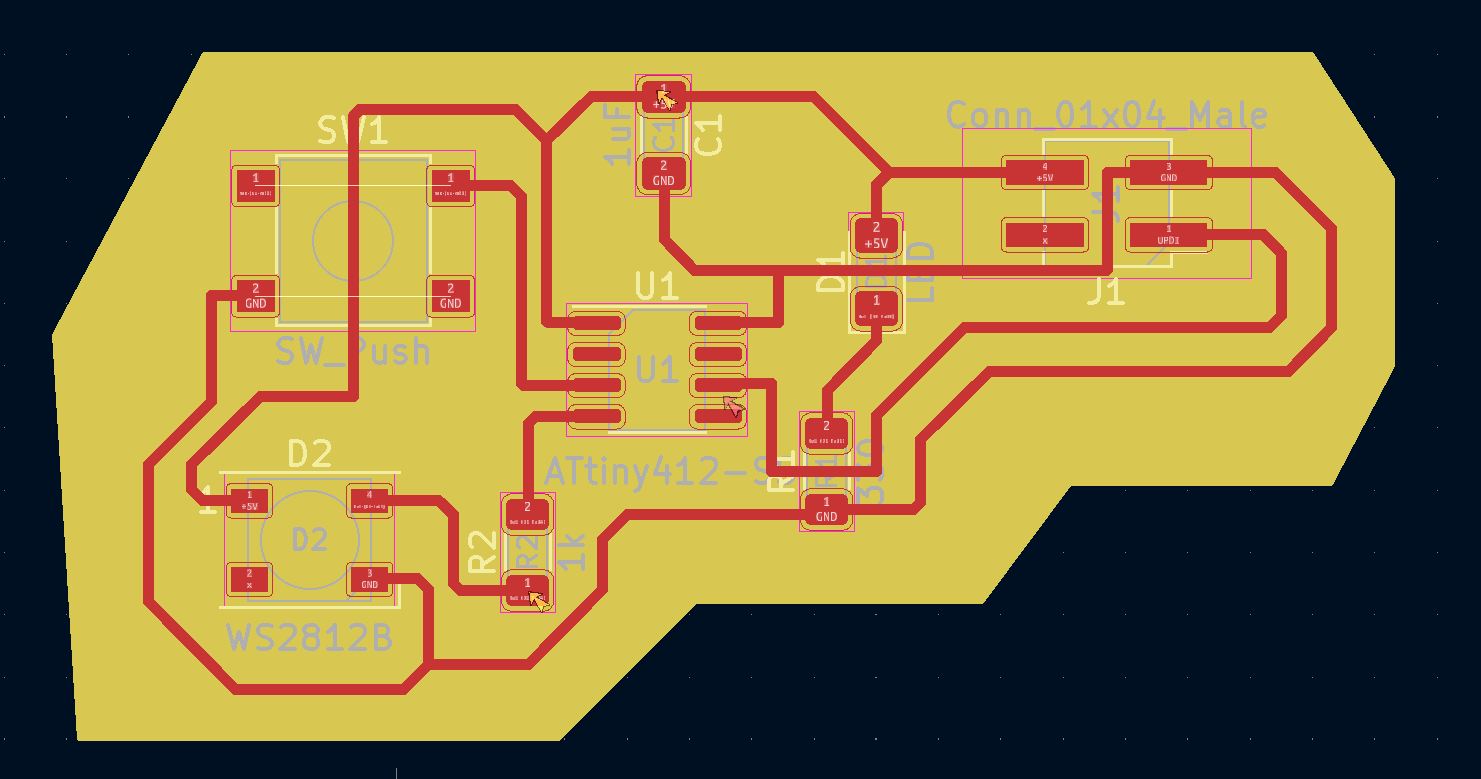
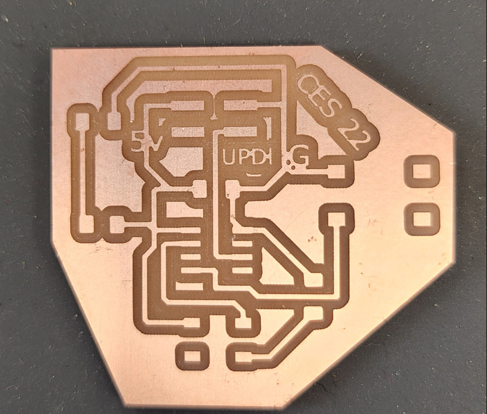
Outline ready to go.
Milling and Soldering
Most of this section is explained in Week 4, but I ran into one particular problem.
We had more PCB material ordered, specifically one sided, but almost all of it came in bowed. It was so bad it was easy to see before we even got it out of the packaging, and it just rolled around on the table when we laid a piece down. This is a huge problem when trying to mill our boards.
For one, if the material doesn’t lay flat, then the tape can’t hold it in place while the tool is moving through it, and it can pull off the sacrificial part. This happened to Garrett about halfway through his board. It can also potentially break the endmills. Luckily, the endmill survived, but the board did not.
It also makes it difficult to make even cuts with both the traces and with milling the board out of the remaining material.
After looking around, I was able to find some smaller pieces that were buried under some other bits and bobs, and the part wasn’t bowed too badly. When I taped it down, I made sure to push down as much as I could to get it to lay flat.
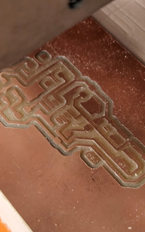
The toolpath was much deeper on this board than on others I’ve done. One the plus side, it means there’s no chance of my traces touching.
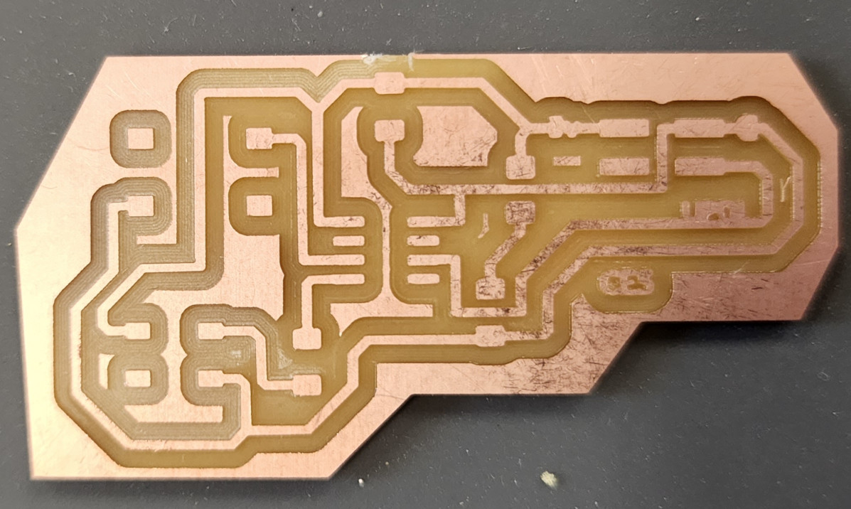
It’s a bit beat up because I found the material on the bottom of a bin.
I included a NeoPixel on this board again, and made sure to double check the orientation of the pixel before soldering it in place.
![]()
The notch indicates ground. Now I’m ready to commit.
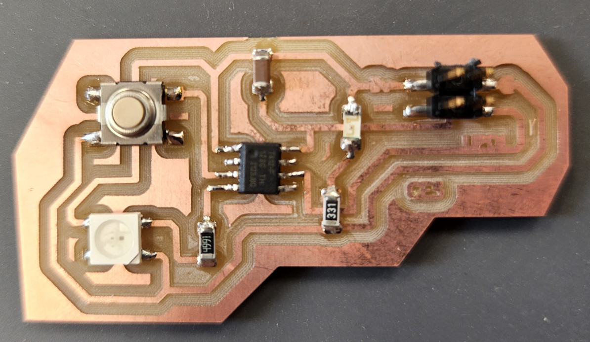
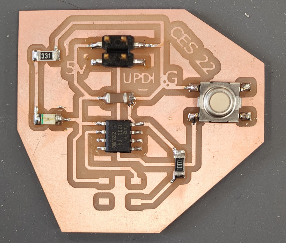
I think I’m getting better at soldering!
Programming
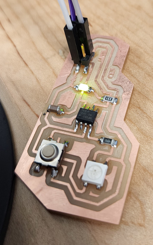
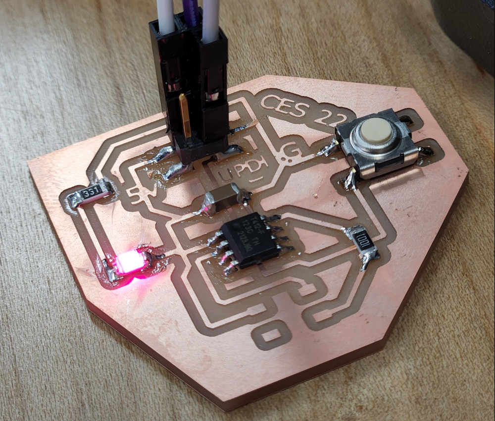
Not gonna lie, I was a bit nervous to plug this in, considering how the LAST board ended up, but hey! It worked!
![]()
It changes colors!!!!!!!!
Troubleshooting
Let’s just say there was a lot to troubleshoot. I am. Not. A good programmer. Maybe eventually, but right now? Nope.
Group Project
The link for the group project can be found here.
A big portion of the group project was troubleshooting my board. After trying multiple programs and tweaks, we used the oscilloscope and micrometer to double check the physical aspects of my board. I recorded and wrote down what we tested on my board, and took pictures.
The First Attempt: A Failed Adventure
This section covers my first attempt. I didn’t document it well and it didn’t turn out much better. I did learn a lot from it though, so the second try went much better in some places, and not at all in others.
Schematic Attempt One
This section covers my first attempt. I didn’t document it well and it didn’t turn out much better.
I’m not unfamiliar with schematics; I see them at work on a regular basis. I’ve worked with them a couple times, but it was early in my apprenticeship and it was more confusing than helpful.
Schematics don’t make a lot of sense to me, mainly because they’re very abstract. I understand that it shows the relationship between the components, but it doesn’t show where they are PHYSICALLY. I’ve heard people call this a blueprint and this is very far and away like a blueprint.
Traces: Puzzle Edition, Attempt One
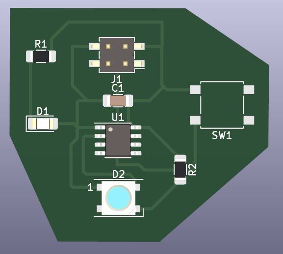
I laughed. It’s so inefficient, but it’s my board. It’s pretty cool that it has the ability to show a rendering of the board, but it wasn’t able to display the button. This second try is not any better, except I tried to make a slightly better outline, but I’m pretty sure this is worse, lol. But it’s mine, so let’s move on to the next part.
Time to Make the Thing
Inkscape
Same procedure as before, in Week 04.
I’ll admit, I’m impressed that it looks this good for a first attempt.
Making My Attempt
And now we’re back to mods. I felt more comfortable using it, and even remembered the different steps to fill everything in. It doesn’t sound like much, but it made me feel like I was firmly retaining some of the information from prior weeks.
The board took roughly 8 mins to mill the traces, and 2-3 mins to mill the outline.
Soldering My Attempt
Cleaned up and ready to go.
First, it took a half hour to find all my components. There is a system in the soldering lab that uses cubbies that have a letter and number designation, bit I don’t have access to the master list. I had to rely on what I remembered from watching everyone else pull out components, and a lot of hunting through the rest. The hardest part was finding the ATTiny, but in the process I found a button that would work.
Initially, I had a button from one of the Arduino kits and was planning on bending the leads and trimming them to size, but this is much easier. Hopefully it will work just as well.
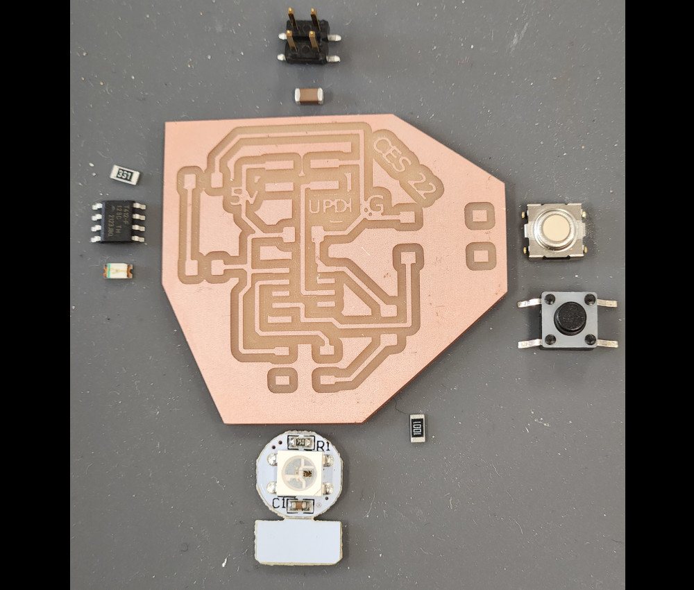
The original button is below the one I found while gathering the other components. I’m not sure if it will work. The pads are almost too far apart to connect, but I’ll do my best.
Same process as before, but I almost forgot to wet my sponge. Whoops. Moving on.
For the most part, soldering went smoothly. I’m comfortable with the process, with a couple hiccups, but then I hit a snag. I have a NeoPixel that I want to add, but the base is not meant to be soldered by hand. Garrett showed me his arrangement with using wires to connect it, and I attempted the same, except I couldn’t find any wire strippers that actually pulled the plastic casing off the wires I found. All it did was scrape off a bit of the outer layer and make them look beat up and gross.
Well, ran into an issue here.
I learned a method to strip wires from work years ago that used a razor blade to score a mark across the plastic. Then you bent the wire at the score, stretching and hopefully breaking the bit of material that was left, exposing the wires inside. Once started, it was just a matter of working your way around the wires until the plastic was removed. I can probably do the same with these, but the wire is very thin, so I have to be extremely careful. It’s also quite tedious, as I’m sure you can imagine.
Connecting My Attempt
This part was both exciting and nerve racking. I had to make sure I connected everything correctly so I wouldn’t fry my board and have to start all over again.
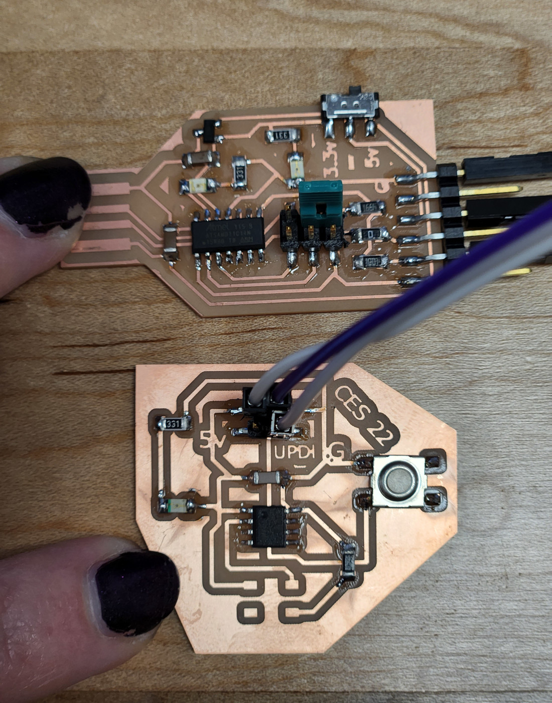
I referred back to this picture to make sure my connections were in the correct position. Purple was ground, white was voltage, and the light grey was data. Fingers crossed I did this right.
You have no idea how excited I was that it worked. I actually gasped out loud.
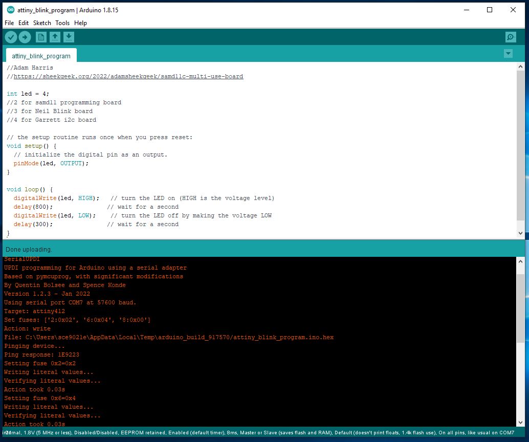
I then tried testing it with the program Garrett had used from Adam (going down the rabbit hole). I copied it to the Arduino program and checked that all the settings were still the same. I then verified and uploaded it.

It didn’t blink. :(
I’m not sure what to do here.
Just for kicks and giggles, I tried the other program from Garrett’s site that was a modified code from Arduino’s tutorial. I changed the currentState from LOW to HIGH since my LED was always on, and adjusted the if else statement as well.
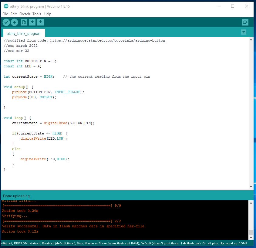
Nothing.
So. Excitement is fading, but we’ll figure it out.
First things first, I went to the button tutorial page to read exactly what I needed to do.
After reading through the tutorial, I copied the test code, but I noticed that the pin listed for the button was different from what I had designed. I checked the pinout (which I first Googled, then found on Adam’s site, which led me to Spence Konde’s GitHub. From here, I confirmed that my pin number was actually 2 instead of 7, but just to test my theory, I tried to verify the code as is and got the error message that it couldn’t find the pin listed. I then changed it to “2” and it compiled just fine.
Please work, please work, please work…
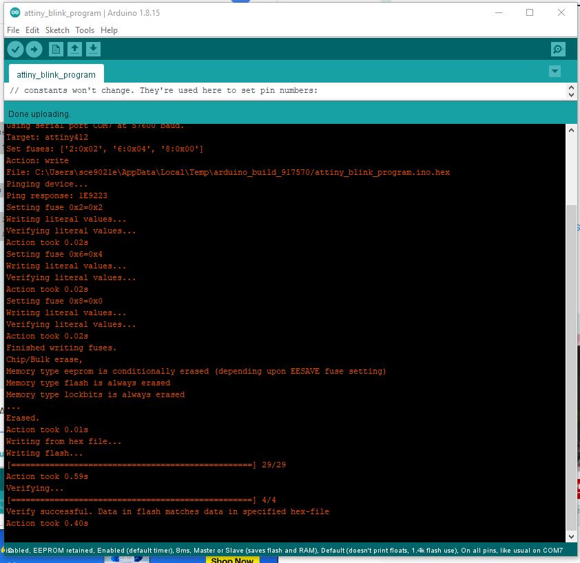
It didn’t work. I don’t know what that first program did, but I’m hitting a wall.
Files
Here are the files for my board, including the .png and .svg files, and the KiCAD files.
And here are the files for my second attempt, with all the same files as the first round.