Week 4: Electronics Production¶
This week I learned to mill, furthered my skill in surface mount soldering, and created an embedded programmer that could plug into my compuer and push code from the arduino IDE onto any chip.
§ Assignment #1: Make an In-Circuit Programmer that Includes a Microcontroller §¶
Source for Workflow¶
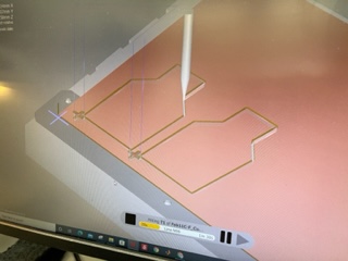
Using the below workflow provided by our Fab Lab, I milled my programmer board. This workflow is shown below:
Preperation Phase¶
Download file
Geber
Eagle
SVG
KiCad Files
Clean the Bed
Use vacuum and remove loose materials.
Wipe down with alcohol
Configure the Bantam Tool
Select tool (end mill or engraving bit) by selecting change
Choose tool under New Tool
Install tool by loosening collet and replacing tool
Click continue
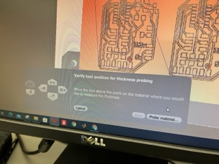
Verify tool position
Locate tool
Material
Select material - generic or FR1
Measure the width and height of the conductive material you wish to mill (PCB - FR1)
Enter the width and height values .
Tape down the material use with to mill Use nitto tape (double sided tape)
No overlaps
No wrinkles
Make sure to put away once done
Z Height
Move probe over FR1
Click on Bit Breaker menu choice
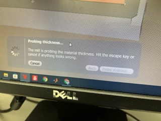
Probe Material Thickness
Check placement
Are you cutting material?
Are you too close to anything?
Align bracket on the left side
Move
Rehome - setting x and y origin
Origin
Loading - use this to load your material
Material Preparation Phase¶
Open file
Placement
Scale
Parts To Mill
Engraving Cutout
Engraving Depth - 15 mm
Milling Tools
Start Milling
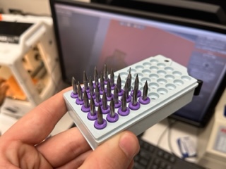
Gathering parts¶
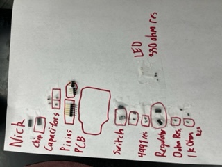
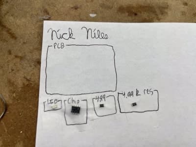
I used a piece of paper to place all of the parts I collected for the programmer I would solder. We were building our programmer based off of the programmer documentation by Adam Harris. Using his parts list, found here I gathered the correct parts and placed/named them on the sheet of paper.
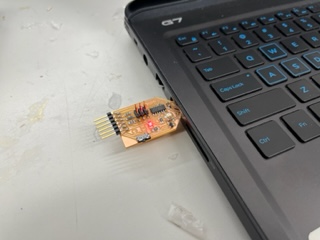
Soldering & Problems with the Board I Milled¶
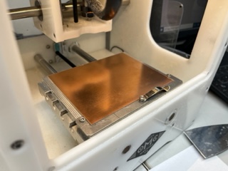
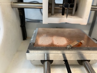
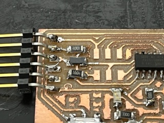
For my first board, I had loosely followed the milling workflow. To mill the boards we had, we needed to use the 0.005 engraving bit and also the 1/32 end mill bit. The bantam mills are designed to let you add both to the parameters of the cut and the machine will stop when the bit needs to be switched. The reason we needed to use two different bits is because certain parts of the trace were very fine and needed a small bit while the outside of the board which would be cut out needed a stronger larger bit to cut out.
Instead of putting in both bits into the menu, I did the trace cuts and the border cutout seperately in different cuts. What this did was give me super fine traces, and while it looked very clean it made the space between traces incredibly small. I began soldering my board that I did with this settings using the schematic found here once more by Adam Harris.
By the time I got to here, I realized how difficult and overly complex I had made this simple board by cutting the space between the traces so small. I had tons of solder bridges forming and it was incredibly annoying. I gave up on this board and went back to cut a new board.
New Board¶
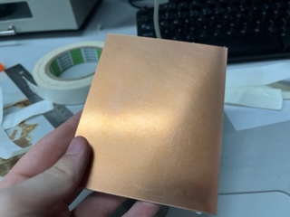
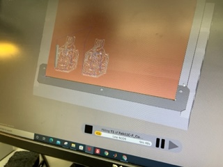
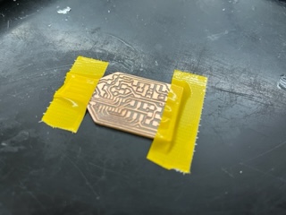
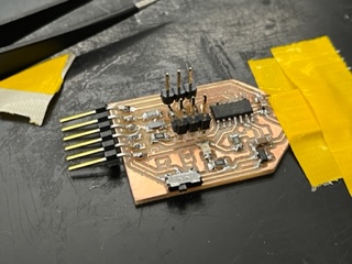
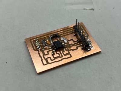
The difference this time is I cut my board with both tools in the same file instead of cutting the trace and outline seperately. This resulted in this cut:
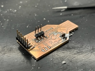
I re-gathered missing parts I needed and began soldering on this new board. I began with the chip. My strategy for the chip was to tape it down on one side and begin soldering the legs as the chip was perfectly held in place. It made it very easy to get the most complex part down.
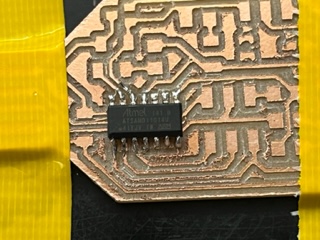
I Immedietly noticed the difference in soldering with this board versus the last, and I was very happy I redid my board. I continued soldering each component.
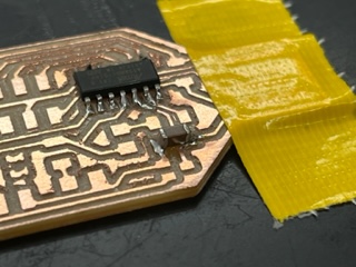
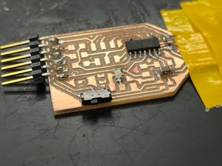
Finally, I finished soldering and it was time to work on the software side.
The Software Side¶
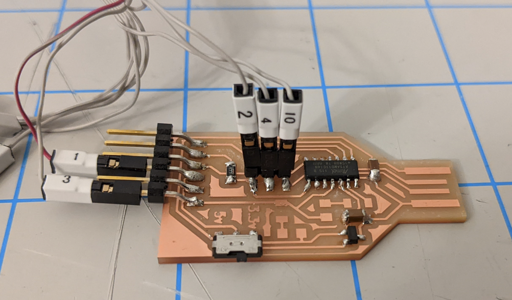
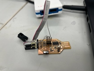
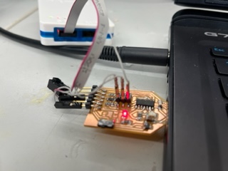
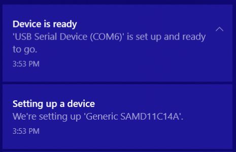
In our lab, we have a device that we plug our jumper wires into from our board based on this image here, the purpose of this is to inject code into the chip on our board so that the device can be accsessed through the command prompt on our compuer when the device is plugged into a USB port. Once it is plugged into the USB port, we download files from here and open command prompt. You cd to the directory of these downloaded files, then run edbg-windows-r24.exe -bpv -e -t samd11 -f sam_ba_Generic_D11C14A_SAMD11C14A.bin. If you don’t get an error, you can continue. For me, I continued to get errors even after changing the voltage switch on the board and making sure the jumpers were correct. I ruled it down to be that my board’s cuts for the traces were too rough and it was resulting in a short that I wasn’t able to find, and as a result, I milled a third board.
The Third Board¶
This time around, I correctly followed the workflow, used the 2 bit settings, and lastly made a new change. In the advanced settings, I changed Trace Clearence to 1.5mm, what this does is it cuts that distance outwards from each trace if that space is not another trace, essentially getting rid of extra unneeded copper on the board that could cause shorts or bridges. I soldered this board just as I did the other.
Software for the Third Board¶
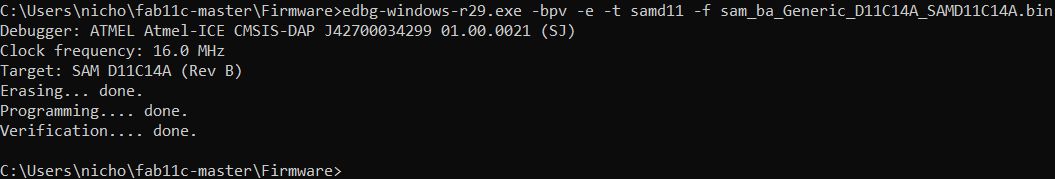
I began by downloading the repository from the link listed earlier, then I used the command c:\users\nicho\fab11c-master to cd to the directory of the firmware. Then, I began connecting the correct jumpers of the SAM box to my embedded programmer. Finally, I ran the command edbg-windows-r24.exe -bpv -e -t samd11 -f sam_ba_Generic_D11C14A_SAMD11C14A.bin, and got a positive result.
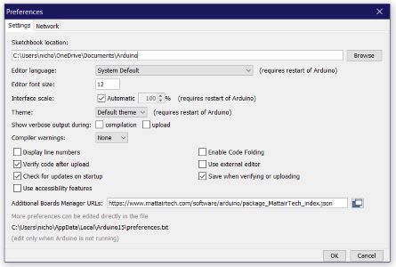
Next, I opened the Arduino IDE and went to the preferences. Then I pasted https://www.mattairtech.com/software/arduino/package_MattairTech_index.json into the Additional Boards Manager section.
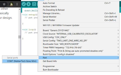
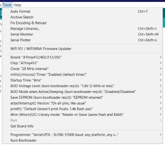
I then went into the Boards Manager section and searched for SAMD and selected and installed the MattairTech one. After that, I setup the correct settings under the Tools menu.
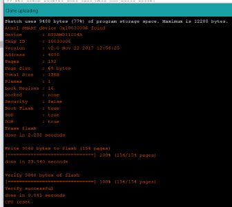
Lastly, used the code from Adam Harris’s website to test uploading code from Arduino. This came out with sucsess, however, the builin LED on the programmer did not flash like it was supposed to, but the console output in Arduino gave me confidence that it worked.
int led = 2;

// the setup routine runs once when you press reset:
void setup() {
  // initialize the digital pin as an output.
  pinMode(led, OUTPUT);
}

void loop() {
  digitalWrite(led, HIGH);   // turn the LED on (HIGH is the voltage level)
  delay(1000);               // wait for a second
  digitalWrite(led, LOW);    // turn the LED off by making the voltage LOW
  delay(1000);               // wait for a second
}
Even though the LED didn’t work, I decided to keep on and move on to making it a programmer regardless.
Making it a Programmer¶
Next, I pasted in this code:
void setup() {

   SerialUSB.begin(0);
   Serial1.begin(57600, SERIAL_8E2); //Adjust baud rate and use SERIAL_8N1 for regular serial port usage
}

void loop() {
   if (SerialUSB.available()) {
      Serial1.write((char) SerialUSB.read()); //Send stuff from Serial port to USB
   }
   if (Serial1.available()) {
      SerialUSB.write((char) Serial1.read()); //Send stuff from USB to serial port
   }
} //end loop
And uploaded it to my programmer board with sucsess.
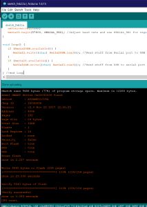
With this, my board was now a programmer!
Creating a Blink Board¶
To begin, I layed out all the needed components on a sheet of paper I labled by part based off the schematic we were given. This schematic was provided from Adam Harris’s Website at that link.
I then went through the process of soldering each component. I was using one of the Lab’s soldering irons, meaning it had a massive tip and was very worn and used. Doing the soldering with this iron took FOREVER and about an hour to finish the board.
Programming the Blink Board¶
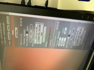
Finally I needed to program the blink board through my embedded programmer. I hooked jumper wires from my embedded programmer to my blink board correctly and plugged the programmer USB into my computer, then inputted the following tool settings in Arduino:
Lastly, I uploaded the arduino blink code with sucsess to my blink board. Here is a video of the first working version:
And here is a video of me greatly increasing the speed of the light flash on the board to show I can change and reprogram the chip easily:
§ Assignment 2: Group Work (Characterizing the Design Rules Our In-House PCB Production Process) §¶
All group work is documented on your group site, found here.