Week 9. Electronics Production (Mar 15)
Week 09 Assignment - make an in-circuit programmer that includes a microcontroller:
-
mill and stuff the PCB
-
test it to verify that it works
-
extra credit: try other PCB processes
-
extra credit: customize the design
SAMD11C Programmer
This week, the programmer I chose to make was a SAMD11C programmer, since that’s what our main lab instructor, Mr Dubick, had all our lab’s Fab Academy students create.
General steps I took to create a working programmer
-
Milling the board out of a copper sheet
-
Soldering the components onto the board
-
Installing the firmware with Atmel ICE to allow programming
-
Using the SAM chip to act as a programmer
All of the instructions were from the documentation made by one of our instructors, Dr. Adam Harris. Here is some of the notable resources I used, further detail is covered in the next sections.
Board 1
Note: The milling process for each board iteration is about the same, and for the later boards I talk mainly about the differences in the process from Board 1.
This week, we had to create a circuit board by using the milling machines we have in our lab. Since I had never actually used these machines before, this step turned out to be quite the challenge and I made many mistakes. However, I learned a lot this week and gained valuable experiences on using the milling machines.
To start off this week, I took a look at our lab’s workflow for using OtherMill and Bantam tools. It explained the milling process pretty thoroughly, but I wanted to see a visual example. Thus, I pulled up the photos I had saved on my phone from last week, when Mr Dubick demonstrated the milling process to our whole group.
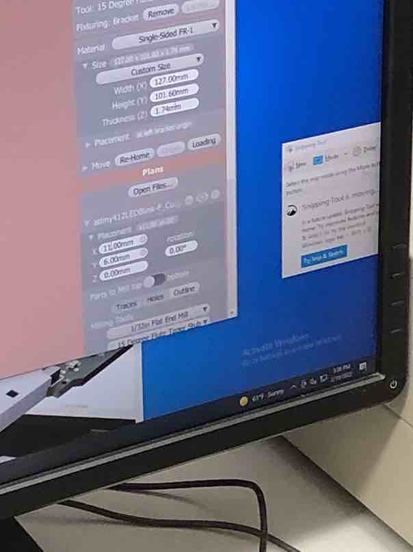
This is a picture of Mr Dubick demonstrating the placement and material sizing settings.
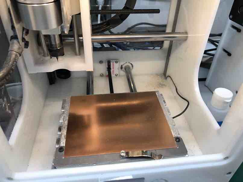
Once I looked at these resources, I thought that I had a pretty good grasp on the milling process. Since our lab has 4 milling machines and 8 students, I paired up with fellow student Jada in order to save time and mill out both of our boards on one design. There was already a copper sheet that someone else had milled that was stuck to the pad, so I took a spatula and pried off the tape. Then I took another full sheet of copper, stuck a few pieces of new nitto tape onto the back, and pressed it down onto the mat. This is what it looked like.
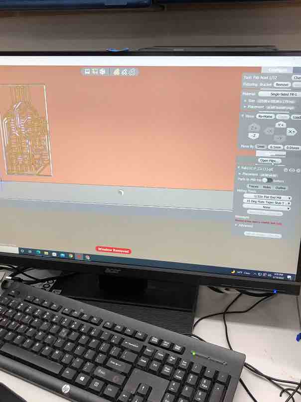
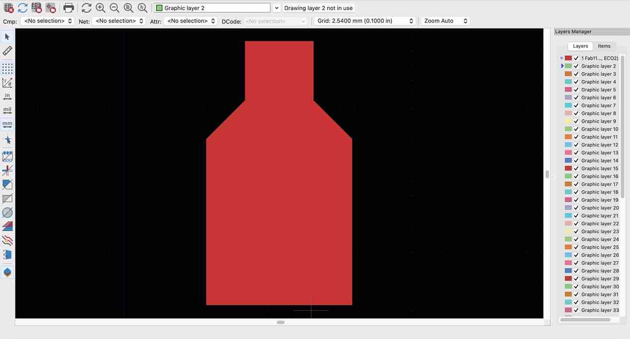
Then I went to Dr. Harris’s gitlab page, and went to the Gerbers folder. At first, I only downloaded the design file called Fab11C-F_Cu.gtl, which was a mistake since it was only the gerber file for the traces and not the outlines. Then, when I was about to begin setting up the settings for the cut, I noticed that there were no outline cuts, which would be a problem since it would engrave the trace design out, but not cut the design out as a seperate chip from the rest of the copper. This is an example of what the design looked like with the wrong outlines.
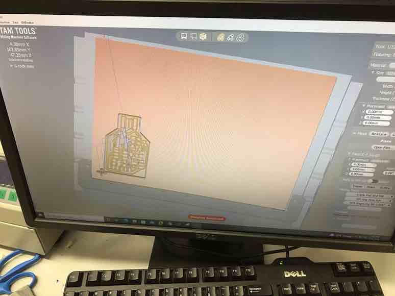
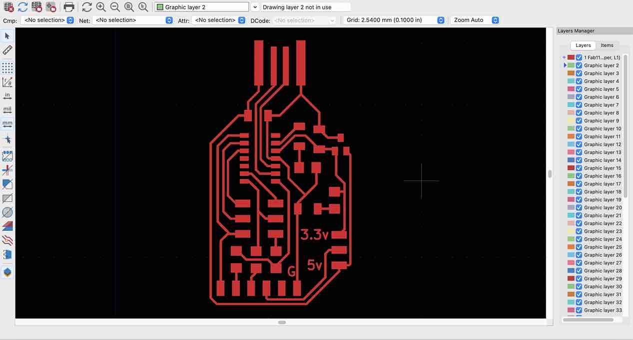
After realizing this, I quickly backtracked and saw the other gerber file included in that same folder, the Fab11C-User_Eco2.gbr file. This is what my design looked like with the correct outlines
To check that it was indeed the correct outline file, I opened the files in my macbook’s gerber viewer. This is what the outline and trace files looked like.
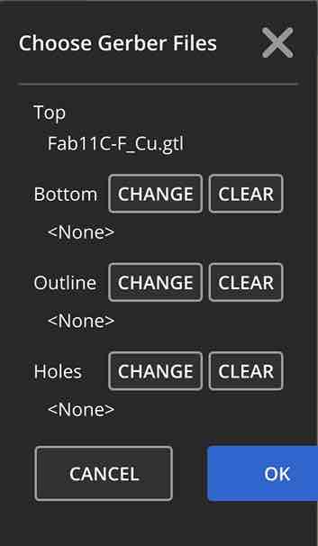
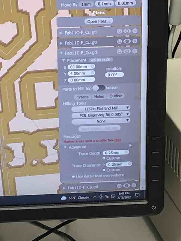
Then I started setting up the milling settings for my first cut by following the workflow. First I went into the Bantam software, went under file and opened up the traces file, Fab11C-F_Cu.gtl. I was prompted with this popup, and made sure everything was none.
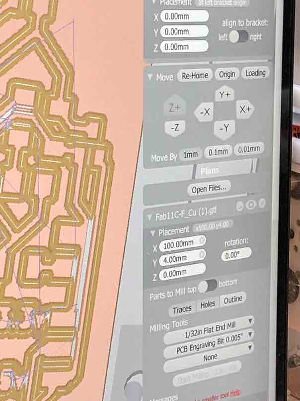
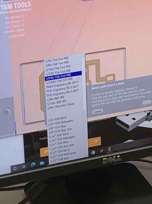
I hit ok and the trace design popped up. Then, I brought in the other file, the Fab11C-User_Eco2.gbr file, using the same method as the other one. Next I had to select the tools I was going to use to mill both the outlines and traces. First I went to the cut settings and turned off holes, since I wasn’t milling any holes. Then, I went to the first dropdown menu, and selected 1/32 end mill, since that was the tool that was best at cutting outlines. Then in the second dropdown, I selected PCB Engraving Bit 0.005 for the traces. Since I wanted to cut on the bottom right hand corner, I made the placement of the cut to be 100 x and 4 y. This is what the settings looked like.
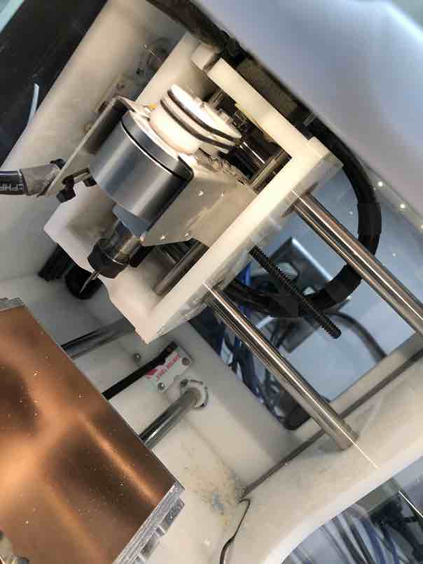
Next, I went and took the two wrenches located on top of the milling machine, and put in the bit. I put in the PCB Engraving Bit 0.005 first since the milling machine always mills out traces before outlines, and I did this by sticking the bit into the whole, and then twisting both wrenches at the same time until the collar was snug.
Then I went back into the Bantam settings, went to the top right corner, and selected the change tool dropdown menu. I selected the option for the PCB Engraving Bit 0.005.
Then, I hit continue. I was prompted with an option to locate the material thickness, which I hit, resulting in this. This allows the machine to know where the tool is relative to the entire machine.
After allowing the machine to locate the tool, the final step was to go under the bitbreakers dropdown menu and hit probe material thickness. Probe material thickness is a step that tells the machine how thick the material you are milling is. This is very important since if you told the machine the material was thicker than it actually was, then the mill would just cut in the air above the material. Before this cut, I made this mistake a great many times, where the material thickness was off and so the machine would just hover in the air. This was another milling attempt I did this week that failed because I did not probe the material thickness correctly.
Also, if you told the machine the material was thinner than it actually was, you would not get the thickness of cut you wanted. This is what probing the material thickness looked like.
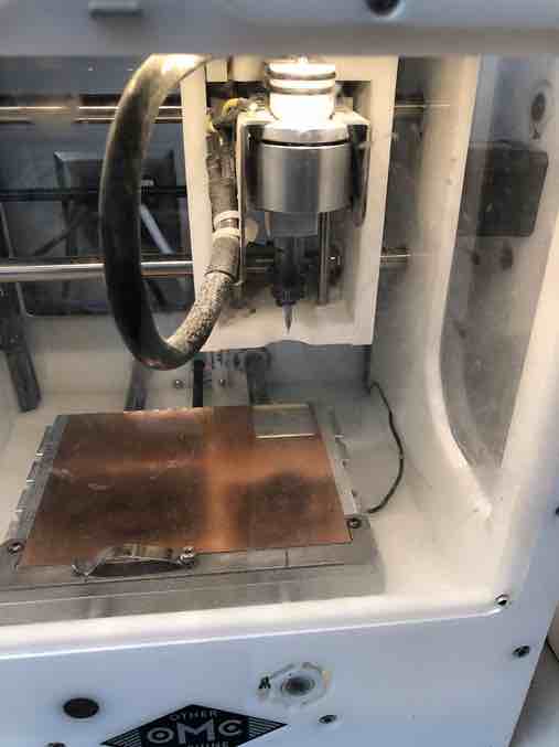
After probing the thickness, I was finally ready to begin milling my copper by hitting mill all visible at the bottom of the settings menu. My first mill took over an hour for a number of reasons. - I was milling out two boards since Jada and I were milling together, - I was using the “slower” milling machine compared to the others, which I was later notified of.
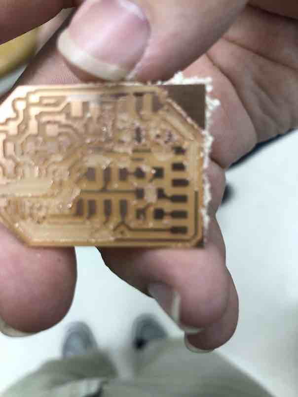
After the mill, I used the handheld vacuum, took off the acryllic cover, and vacuummed up the dust and debris on the pad and inside the machine. This would prevent painful copper splinters when I went to go take the board out. While I had gone through lots of effort in setting up the machine, this mill ultimately failed. This is a picture of the result, and as you can see, most of the traces are a shiny reddish hue, but some of the traces take on a lighter yellow dull tone.
The shiny red indicates traces of copper that were milled properly, and the lighter yellow meant that the mill failed and the traces wouldn’t work if you tried to solder them. Since it failed this meant I had to remill all over again, and I had to do this many more times throughout this week, which taught me perserverance and the spirit of “Fab Fun”.
Board 2
While Board 2 also ultimately failed, I would still consider this improvement since the whole process was much faster and closer to a working mill the second time around
First of all, after the failed mill that happened last time, I pondered why I had failed and began debugging, which led me to a few potential answers. The first thing I did was check my board design, so I went back into Dr Harris’s folder and reopened both the trace and outline gerber files to check if they were correct. I found that they were the correct file, so I went back to the bantam software and thought maybe I had configured it wrong. I went through the entire setup process again, from positioning, changing the tool, locating the tool, and probing the thickness. For example, this is another video of me probing the material thickness.
I came up with two major discoveries which I put into practice with this milling iteration. Firstly, I hypothesized that the reason the traces had failed to be milled last time was because I did not change the trace thickness and trace depth. Last mill I did not change these settings, so they were still the default values of 0.2 and 0.2 respectively. To mill out wider traces and have a higher chance of succeeding, I reasoned that I just needed to make the trace width larger. Thus, I went under the advanced dropdown menu, and modified the trace depth and trace clearance to 0.25 like so.
My second big discovery was that in order to properly probe the material thickness, you had to move the bit over the portion you actually wanted to mill. What I had been doing before was just probing the thickness over a random portion of the copper board, since I assumed all the sections of the board were securely fastened evenly with nitto tape, and thus would have the same material thickness. I’ve learned from this process to never assume anything and don’t leave anything up to chance. Then, once I hit bitbreakers -> probe material thickness, I made sure to use the arrow keys and position the bit over the part I was going to mill. This time, it gave me a lower thickness value than the last time, which fully explains why the machine was just hovering before. It’s because the machine thinks the material is more thick than it actually is, and so by hovering, the machine thinks that it is milling something, when it really isn’t. This discovery resolved that issue immediately, and this is a picture of the settings of my second mill.
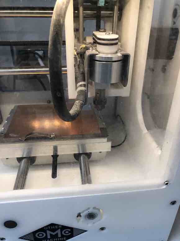
Once I changed these two parts, I went through the same process to mill out the board by hitting mill all visible. This is a picture of the board before the actual milling began.
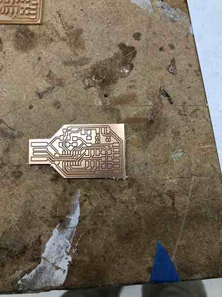
Once I vaccummed the area and used a spatula to pry off the copper sheet, this is what resulted from that mill.
As you can see, this board has much less of ripped traces than the previous one did, which means that this improved the quality of the board, However, you can still see pale spots dotting the board here and there, and the thing about electronics production is that your board has to be nearly perfect, so no ripped traces are allowed. Otherwise, there is no way for your electronics to connect with each other as the ripped traces provide a break in the circuit. With this board however, it only took around 20 minutes to mill out, compared to the hour it took to mill the other one. Although the board wasn’t the fastest or the best, I still felt accomplished with my improvement. Still, it was a failed board, and I would have to remill a third time.
Board 3
Just like the last time, this board was substantially better than the previous iterations. Not only did the milling of the board actually work, but the traces were noticeably much cleaner than previous ones. However this baord was still not my final iteration due to issues with soldering and trying to program.
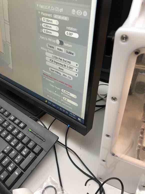
Between milling this board and the previous one, I had again made a revolutionary discovery, which was that there were some parts of the board that weren’t being milled at all. They could not be milled by either the PCB Engraving Bit or the 1/32 end mill, because they were too large of a tool. This meant that I wasn’t actually milling everything that I wanted, and this was yet another issue. Once I reconfigured the design using the same methods as before, I noticed an error in the settings page that looked like so, telling me that I needed a smaller tool in order to mill the small pieces of the board that were being left out.

Thus I needed a third tool, and I spent a while looking through the drawers for the right tool to use. Luckily, a fellow fab student Aarush pointed me in the right direction towards the 1/64 end mill, which he had used to make his board work. Thus, I followed all of the previously mentioned steps for milling, evetually arriving at the step where you have to chose which tool to use. Under the third dropdown menu for each mill file, I selected 1/64 end mill. Right away, the error message went away, and the red spots on the mill preview went away as well.
Note: In this image the middle dropdown for 30 degree eng wax is incorrect, I realized this after taking the image.
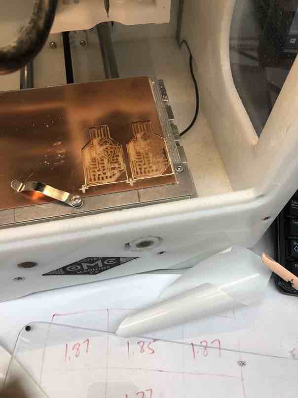
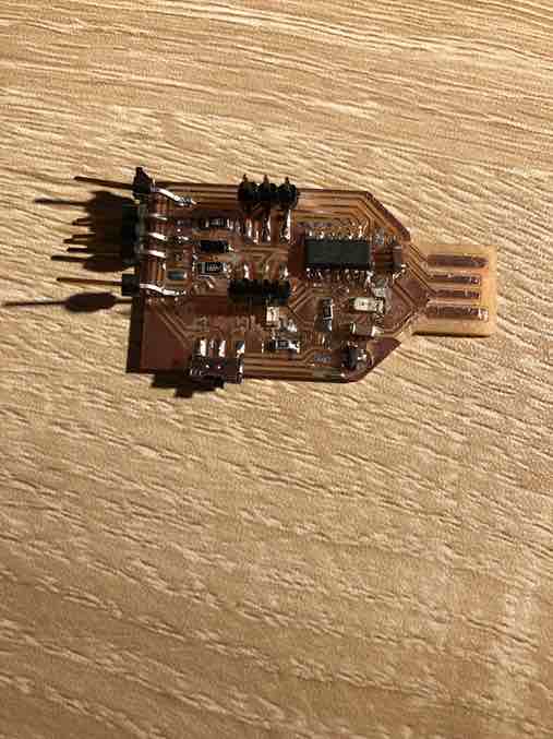
When I milled out the board and vacuumed the dust off, the board turned out like this. As you can see, the traces looked much, much cleaner than before, and I was lucky enough to have none of my traces rip
Now it was soldering time. While I do have some prior experience with soldering, it’s not nearly as much as some of my fellow students have. However, the surface mount flag that will be included in the week 0 documentation was great practice for soldering. The first step in soldering was to find all of the components, which I organized on a piece of paper and taped them down so that nothing would be lost.
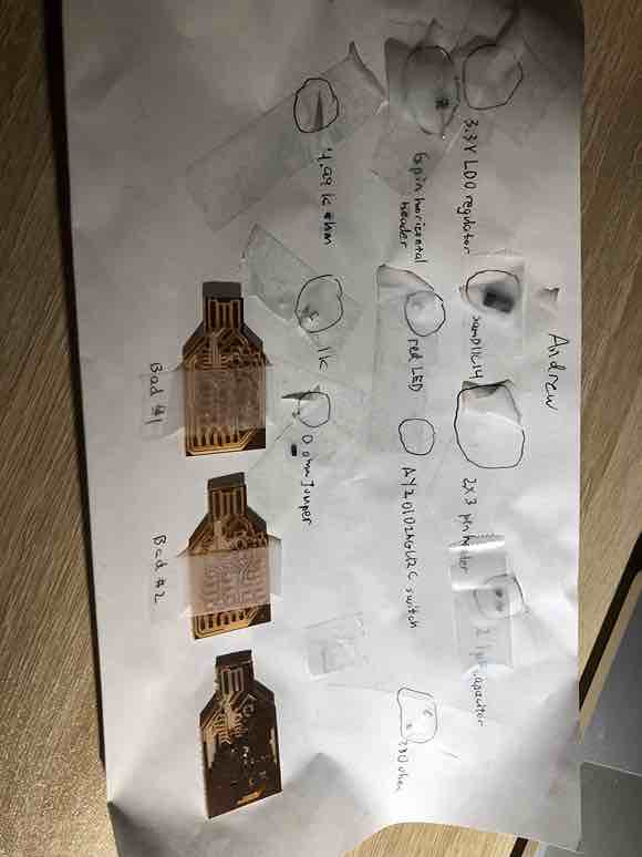
I then went back to Dr. Harris’s website and found the Bill of Materials for the SAMD11C board. That BOM was still missing a few of the components, so here is a list of all the components I used on my board - 1 6 pin horizontal header - 1 SAMD11C14 microchip - 2 3 pin vertical header - 2 1µF capacitor - 2 red LEDs (color doesn’t matter) - 1 AYZ0102AGRLC switch - 2 330 Ω resistors - 1 4.99K Ω resistor - 1 1.2K Ω resistor(I swapped this out for a 1K Ω resistor) - 1 0 Ω jumper
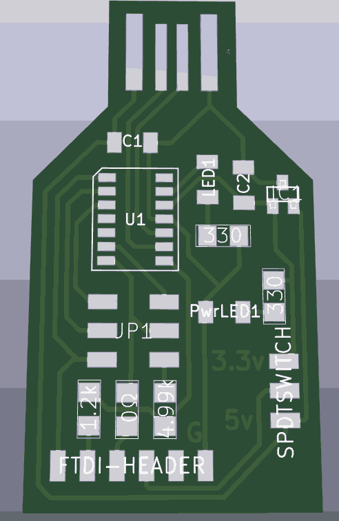
Now that I knew what to solder, I had to figure out where to put everything. I went back to Dr. Harris’s site and found this render file, which showed me where to put each component on the board.
Next came the actual soldering. While I am able to solder both surface mount and through hole, I would say that soldering is currently not one of my strengths, something I primarily attribute to lack of experience. However, I am getting much better at avoiding mistakes like bridges and cold solder joints as I progress through the weeks of Fab Academy, and getting better at soldering is one of my main goals in Fab Academy. Currently, I prefer the method of soldering down one pad, using tweezers and the iron to melt one side of the component in, and then soldering the other pad down. I use this method with components such as LEDs, capacitors, and resistors, but with more complex components I often modify my strategy and try new ways. For example, with the six pin horizontal header, I put solder on all of the pads, and then tried melting each joint down the line.
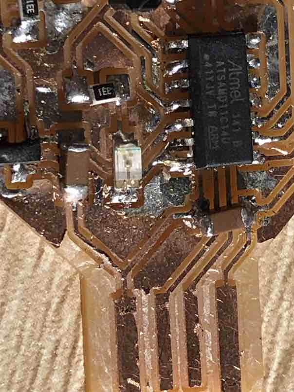
Since I don’t have as much experience, I often have solder bridges and/or cold solder joints with many of my components. For example, in this picture, you can clearly see that the solder on the two legs of the chip are bridged, and the other components look kinda messy due to the poor soldering job.
Because I’ve made so many soldering mistakes, I’ve learned to use two different tools very frequently, the solder sucker and solder wick. The solder sucker is sort of like a suction cup, where you heat up the part you wish to remove and then “suck” it off. The solder wick on the other hand, is a copper wire that you heat up with your iron, the solder sticks to the wire, and then you wipe it away. From Neil’s lecture on electronics production, I’ve learned to put a bit of solder onto the tip of the iron before I use the wick in order to improve heat transfer, making it easier to “wick” it off. I’ve also learned from experience that the solder sucker and solder wick are used for different situations. For example, the wick is better with small bridges, and the sucker is better with sucking large chunks of solder off. This is the finished board after soldering.
The grey spots that you see are the places where I wiped the solder away with the wick. Once I was done soldering, I tried plugging the board in, however I got this error.

My guess is that I have solder bridges in some places which are preventing the board from getting power. Rather than sift through the connections to find which one were bridged and which ones weren’t, I decided to completely redo another board, since this board was kinda sloppy anyway, and I was pretty sure I had ripped a trace when soldering this board. I learned to appreciate the difficulty of electronics: it’s not that the task is physically hard, it’s that you have to be very careful with each step; otherwise one step could set you back at the beginning. To be honest, I was very annoyed that I had to restart the entire process, but in the end I perservered and got it working with the next board.
Board 4
Since our lab’s students had failed so many times, we had all gotten fairly quick at milling out boards. Our lab was also very efficient in that people who broke their board and had to remill would mill out multiple boards in one go, in order to distribute the boards to others who had broken their boards. We all had a pretty good grasp on how to mill out PCBs, but it was just a matter of efficieny and saving time on milling for all of us.
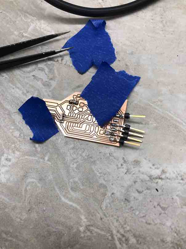
At the time, fellow student Alaric had milled out extra boards, which he so kindly gave one to me. This board was admittedly in worse condition than the one I had milled previously, but it did the job so I jumped right on soldering the components onto the board. The only difference from the last board was that I used a designated 2x3 pin vertical header instead of using 2 3 pin vertical headers. This time with soldering, I did not have as many errors, which meant the soldering took a shorter time. This is a picture of the soldered board.
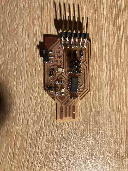
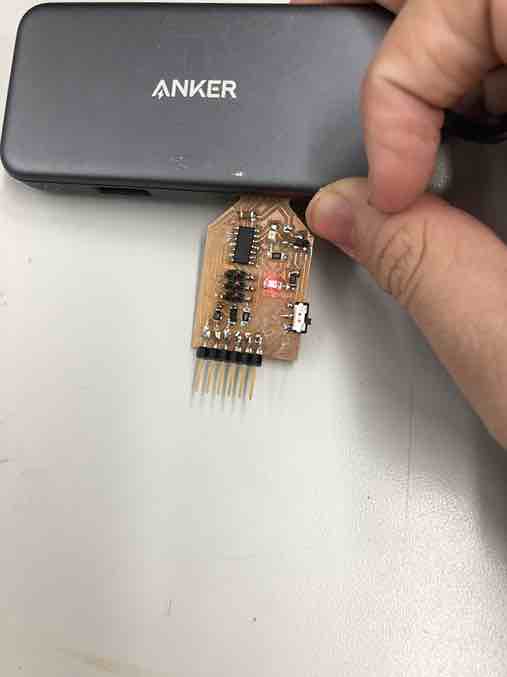
As you can see, less solder is used and the header pins are straighter than the last board, not to mention that this board actually had 6 pins and not 5. The next step was to verify that my board actually functioned. To do that, I took an exacto knife, and carefully shaved off the excess copper at the skinny end, which would cause a disruption if I had left it and plugged it into a USB slot. I plugged the chip into the USB slot, and it worked to my surprise!
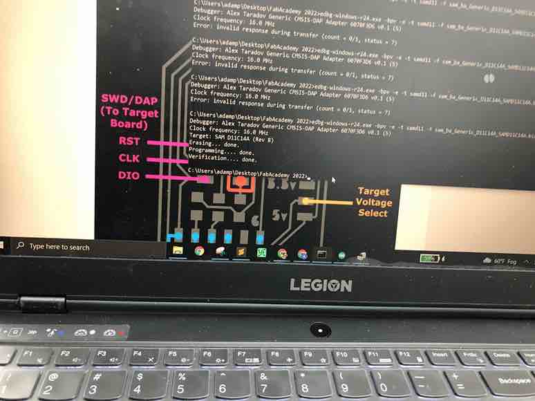
The last step was to turn the SAM chip into a programmer itself, which I did using the instructions on Dr Harris’s sheekgeek page. First I downloaded the edbg debugger tool, downloading the mac r31 version instead of the windows. then, I tried plugging in the Atmel ICE programmer and downloading the .bin file, but I noticed that the ICE wasn’t even recognizing my chip. I thought that I had soldered incorrectly or ripped a trace possibly, so I went back and checked my board under a microscope, but didn’t see anything out of the ordinary. I asked Dr. Harris himself to assist me, and identify what was wrong, but Dr. Harris simply said that the Atmel ICE wasn’t working. This was confirmed by fellow students Pari and Aaron, who also tried using the ICE and could not get it to work.
Since the ICE didn’t work, Dr. Harris helped me turn my chip into a programmer by using his working chip in place of the ICE.
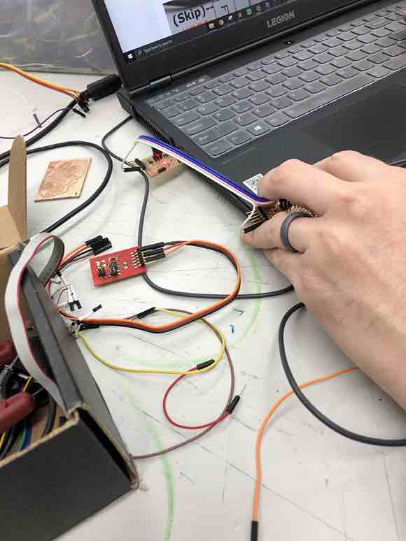
Since Dr. Harris used a windows computer, he pasted in this command into the command line, producing this, thereby proving that my chip was now a programmer and it worked.
Week 09 Group Project
This week’s assignment was to characterize our lab’s PCB milling machines and write up a new workflow on how to use our machines
I worked on replacing the necessary bits when it was necessary to change them out. Our mill required two different bits, the 1/64 end mill for the traces and the 1/32 end mill for the outline. Since the machine always mills the traces before outlines, I used the wrenches to put in the 1/64 bit first, and then when the machine was finished with that, he put in the 1/32 end mill. I also contributed to the “During Milling” section of the group milling machine workflow.
This is the 1/64 bit
This is the 1/32 bit
More information can be found on the group site
Week 09 Files
Click here to access all my files for this week