5. Electronics Production
Assignment: Make an in-circuit programmer that includes a microcontroller:
Blinky
With Breadboard
Before I started Fab Academy, I was showed by (Mr. Dubick) how to turn an Arduino into a programmer for a ATTiny412 chip.
Soldering
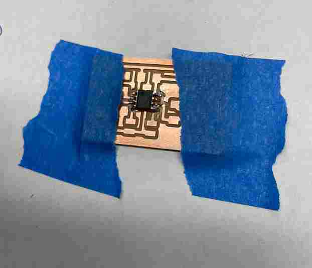
I prepared for soldering an ATTiny412 chip to a simple breakout board. Before starting the soldering, I was shown what a successful chip looked like. I used a breadboard to place the pins in. This made it simple to orient the breakout board onto the pins. I decided to solder the edges first to create a stable surface before soldering the other wholes. After completing this, I had to surface mount solder the ATTiny412 chip onto the board. First, I pre-soldered the board in the necessary areas “note the regions for soldering were small”. Once I finished pre-soldering the used a pair of tweezers plus my soldering iron to hold the chip in place. During this process, I created a few bridges but quickly cleaned that up. After finishing that, I had completed the first step
The soldered ATTiny412 chip was already connected to the breadboard. The next step, check the connection by providing power and coding. Using Mr. Dubick programmed Arduino, I connected the power and ground, the data line to the pin (Note the PIN for the chip isn’t explicitly stated, must lookup on the internet), and the UDPI to the LED (note this is like the data line for a normal Arduino, connect it to the input device) to it I tested the connection and it worked.
Wiring Before Arduino
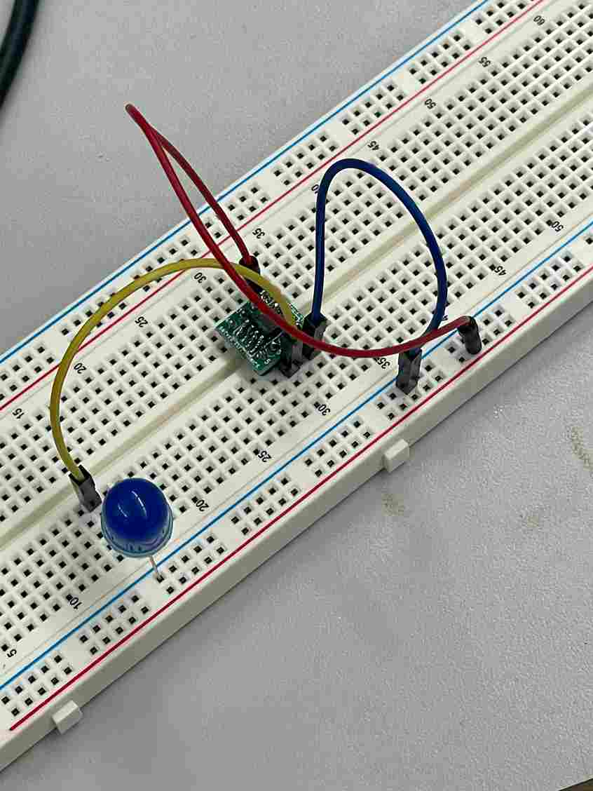
I examined Mr. Dubick’s breadboard first, and before connecting anything together, I looked up the pinout for a ATTiny412 chip. The only parts that concerned me were the UPDI, VCC (or power), the ground, and the pin numbers for the chip (labeled in orange on the picture). I also looked up the pinouts for an Arduino Uno and noted that the UPDI was pin 6, this would be important later. I attached my soldered board to the breadboard and performed the following
- Connected the power pin (pin 1) to the power rail using a red wire.
- Connected the ground pin (pin 2) to the ground rail using blue wire
- Connected the data line pin (which I labed as 4) to the LED using a yellow wire
- Connected the LED long end (power side) next to the data line and the short end (ground side) to the ground rail so they share a common ground.
Wiring After Arduino
After Arduino The next step was to include the Arduino nano. I required three cables, a power, ground and UPDI. Similarly to the breadboard I did the following
- Connected the 5V from the Arduino to the power rail
- Conencted the ground into the ground cable
- Connected the UPDI pin (pin 5) to the UPDI pin on the Arduino (pin 6) using a purple wire.
- Note on UPDI. The Arduino when it becomes a programmer, convertes the code it receives from the computer into code the ATTiny412 chip can understand using the UPDI. Therefore, I have to connect the UPDI from the Arduino to the UPDI of the chip. Then from the data line of the chip it can use that to program the LED.
Before I could program my ATTiny412 chip I needed to install Arduino from the Microsoft store. After downloading, I began the steps to configure my Arduino to see itself as a programmer for the chip. Using this documentation I was able to do the following steps with ease
Installing megaTinyCore Library
- In Arduino IDE, Install the ATTiny Library: Go into File > Preferences > Additional Board Managers > type this url
http://drazzy.com/package_drazzy.com_index.json> Ok - Add the Chip: Tools > Board > Board Manager > Download “megaTinyCore”
Making an Arduino a programmer
- Install UDPI programmer sketch: Click on GitHub Link > Code > Download ZIP > Open > Extract All note (delete “—master” in any file as you relocate the file in. I couldn’t access jtag2udpi correctly because of this)
-
Opening and Configuring “jtag2udpi” : Open the file you just extracted > open “jtag2dupi.ino”, and it should open Arduino IDE with multiple tabs open (DO NOT TOUCH THOSE FILES). Those files contain multiple libraries and functions that allow the Arduino to become a programmer. I plugged my Arduino into my computer and checked two things
-
Port: COM Arduino Uno (may vary)
- Boards: Arduino Uno
Upload this file into the Arduino, this will allow it to become a programmer. Check for success by seeing if the LED on the Arduino flashed twice.
Uploading Code into ATTiny412
- Upload the code needed for LED: I opened a simple blinking code Files > Examples > 0.1 Basics > Blinking. Once opened, configure the pinMode to the necessary PIN of the ATTiny412 Chip, not the Arduino I messed this part up and my board wouldn’t work. Usually, ATTiny412 chips have it at pin4. Next, I edited the tools by going to Tools > Board > megaTinycore > AtTiny412/402/212/202 (don’t choose w/Optibot). Check Port for the correct one. I ran the code and it worked
// the setup function runs once when you press reset or power the board
void setup() {
  // initialize digital pin LED_BUILTIN as an output.
  pinMode(4, OUTPUT);
}

// the loop function runs over and over again forever
void loop() {
  digitalWrite(4, HIGH);   // turn the LED on (HIGH is the voltage level)
  delay(1000);                       // wait for a second
  digitalWrite(4, LOW);    // turn the LED off by making the voltage LOW
  delay(1000);                       // wait for a second
}
Notable Errors I had to troubleshoot with help from Dr. Harris
- Checking the LED long leg is in the power section while the short leg is in the ground section
- Check the PIN is in the right place and it corresponds to the program
- I downloaded the wrong repository and I didn’t all the tabs on my Arduino app. (This is why my Arduino didn’t flash twice and when I tried running the code the first time, I received errors)
With PCB
Soldering
Using this documentation by Dr. Harris I used his PCB design to correctly solder my copper board, that was already milled. I need the following materials
- Milled Copper Board
- ATTiny412 Chip
- LED
- 4.9K resistor (I used a 4.99K)
- 499 Ohm resistor
- Capacitor
- 6-pin SMT header
Looking at Schematics and ATTiny412 Chip
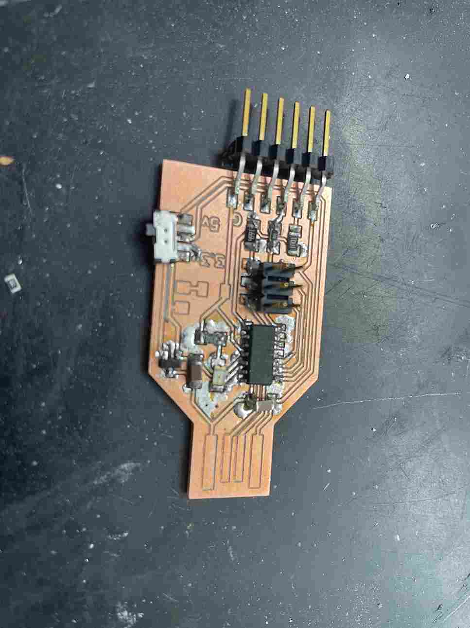
I first began my soldering my ATTiny412 Chip in place. Looking at the schematics and the pinouts for the chip, it was important to note the power on the schematic and the chip. The corner with the indent is the power wire so I souldered that to the top right of the boardwhere the VCC was labed. I then proceeded to solder the rest of the chip by presoldering the copper.
Mistake With Copper
A notable mistake that I made was that I overheated the copper which eventually tore off the copper connected to the second pin from top on the left side. This happened because the copper, which is sensitive to heat, didn’t have enough surface area to spread out the hear from the soldering iron. Causing it to move. Though with instructions from Dr. Harris, this wouldn’t affect the board because the pin wasn’t connected to anything. Also I used solder wick, recommended by Dr. Harris, this greatly helped because the solder would spread uncontrollably onto the copper.
LED
Next was soldering the LED. Since these components have polarity I had to check for the positive and negative charges. Using a Multi-meter, I switched it to the Ohm sign then pressed function key until I saw an arrow with a triangle through it. When pressing the two cables in the correct way the LED should light up. I figured out that the ground was the green doted side. I soldered that into place and was almost done
4.99K and 499 Ohm Resistor
I then focused on soldering the 4.99K resistor into place, this was very easy after practice with the American Flag. This was the same case for the 499 Ohm resistor.
Capacitor
The capactitor was as easy as the resistors, it doesn’t have polarity (at least from what I know).
6-pin SMT Header
Second to last was to solder the 6-pin header. I broke off a larger piece then placed them on the 6 pins to the right of the PCB. I soldered them down with ease then went on to the capacitor
Connecting and Programming
Similar to the first time with the breadboard. I programmed the Arduino to become a programmer, using my earlier documentation. The difference was connecting the wires. Looking at the schematic I found which pins on the header were, ground, power, and UPDI. I connected my power and ground on the PCB to the usual places on the Arduino, 5V and GND using a male to female wire. Similar to the breadboard I connected the UPDI on the Arduino (pin 6) to the UPDI on the PCB.
 ){width=500}
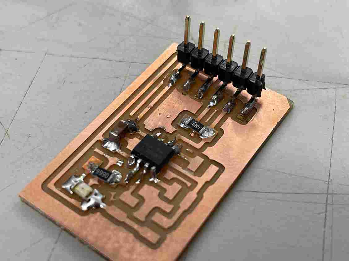
Coding
I had to change my code from the first time with the breadboard. Instead of using pin-6 (ironically the pin I tore off) I was using pin-0. This was easy to tell by using the schematic. I found that pin-0 was leading into the LED so when programming the LED I had to change the pin to 0. I ran this code but I ran into an issue.
// the setup function runs once when you press reset or power the board
void setup() {
  // initialize digital pin LED_BUILTIN as an output.
  pinMode(0, OUTPUT);
}

// the loop function runs over and over again forever
void loop() {
  digitalWrite(0, HIGH);   // turn the LED on (HIGH is the voltage level)
  delay(1000);                       // wait for a second
  digitalWrite(0, LOW);    // turn the LED off by making the voltage LOW
  delay(1000);                       // wait for a second
}
The copper board couldn’t receive the code. I looked at the PCB to see if I soldered anything wrong. I thought it was fine until I noticed that the 6-pin header wasn’t correctly soldered and was infact, soldered in only 1 pin. I went and resoldered them and ran into another problem, the code wasn’t uploading. I realized that my board wasn’t correct, and when trying to switch it to the ATTiny412 chip my computer seemed to delete the board directory. I had to reinstall using my earlier documentation on installing the chip. I did this and I still received problems, then after checking the settings I realized that it was programmer; it wasn’t set to jtag2udpi. I fixed this then ran the program and it worked.
Side note on the design of the PCB. It is designed so the pin actually becomes a ground. The best way to explain this is with an analogy from Mr. Dubick. Voltage is like a waterfall, it needs to start high then end low. When pin-0 is set to high on the program, voltage isn’t able to flow through, meaning the LED won’t light up because we have two high grounds. When the pin is set to low, I have a difference, so the voltage flows throught the LED making it light up, therefore, it becomes a ground in its own way, this then flows throught the chip to the label.
Programmer
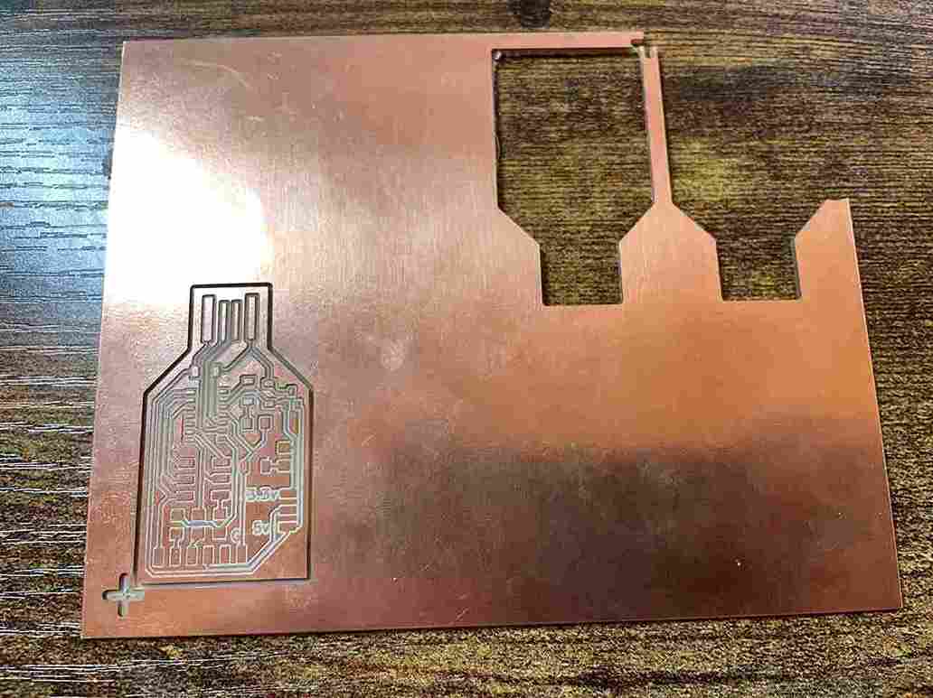
Using Dr. Harris’s documentation I found the PNG for this PCB design that used a SAMD11C microcontroller, to create an in-circuit programmer.
My Failures
Milling
I loaded the GLT file found in the documentation into the Bantam Tools software and started the milling process For most of the PCB’s I either used a 1/32in flat end mill or a PCB engraving bit 0.005” on the first day. I followed the steps below to prepare
- Upload the file
- Have two files and have them operate as separate cuts, does the same process, (e.g one engraves, and one cuts)
- Usually, select both tools and the file will clear all red
- Change the bit on the machine to what you want
- Change the bit on the machine to what you had, and it will ask you to locate the tool (make sure it locates off the board so the material thickness when probing isn’t 0.00)
- Rehome the machine to make sure it locates the tool,
- Hit probe material thickness (there is variation between certain parts on the copper. Make sure you probe where the cut is going to be), copper should usually be between 1.75 and 1.93
- Hit mill all visible
- Once the first bit is done engraving, the computer will prompt you to change the bit to the one you already inputted then it will ask you to locate the tool, hit locate and the PCB is done
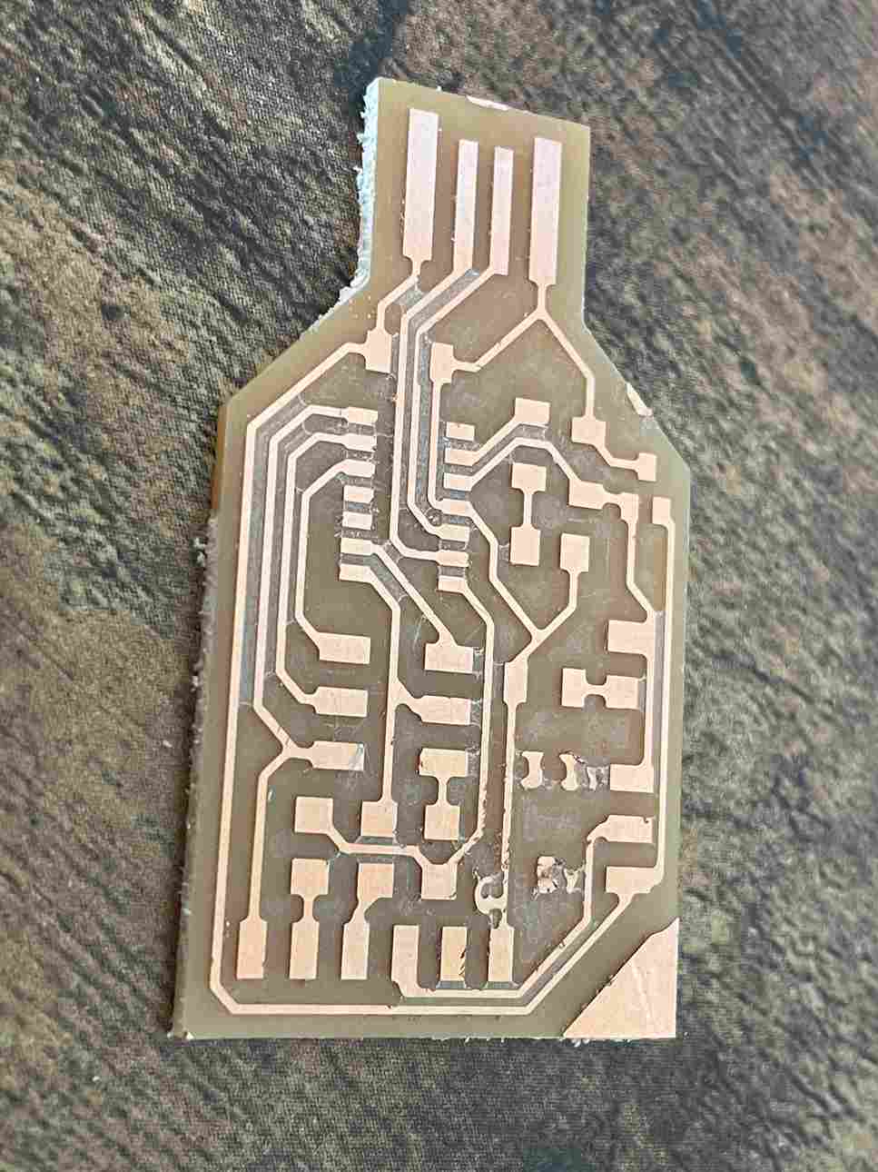
PCB #1
Bits
- 1/32in flat end mill
- Inputted a 15-degree flute taper stub (I used a PCB engraving bit 0.005”)
Settings
- Trace Depth: 0.20
- Trace Clearance: 0.20
This was my first board, so I inputted the bits separately instead of at the same time. I did this because I wanted the machine to engrave first then cut through. Although when I put in both bits, the engraving and cutting bit, the cutting bit would be shown to operate first even with me putting in the engraving bit first. Mr. Dubick said that this doesn’t matter, and the machine will engrave first then cut. I still proceeded with importing the engraving bit first and having that engrave the whole board. I then changed out the bit, probed material thickness and ran the outline cut as a separate mill.
The results looked good but the board in terms of soldering was hard. There was no danger of the traces ripping but when comparing it to other boards, I didn’t think it would be functional. I set this board to the side and milled another one.
I would eventually come back to this one after PCB #2 and PCB #3 didn’t work because I had no other options. The soldering was looking good, there was extra, but the board still looked good. I asked Dr. Harris to look at the board and he saw multiple errors such as bridges, possible short circuits, misaligned components, and unsoldered parts. I asked if the board was salvageable, but he recommended starting and milling a new one.
PCB #2
Bits
- 1/32in flat end mill
- PCB engraving bit 0.005”
Settings
- Trace Depth: 0.20
- Trace Clearance: 0.20
For this I listened to Mr. Dubick’s advice and imported both bits into the Bantam software. The process was much easier because I didn’t have to rehome and re-probe the material thickness. It just prompted me to change the bit and locate the bit.

This board looked promising but there was excess trace between some of the copper. I still attempted to solder it, but I ended up ripping one of the traces connecting the SAM microcontroller.
PCB #3
Bits
- 1/32in flat end mill
- PCB engraving bit 0.005”
Settings
- Trace Depth: 0.20
- Trace Clearance: 0.25
Dr. Harris noticed that a lot of my boards had a lot of excess traces that could short out my programmer. He recommended using a trace clearance of 0.25mm for the PCB engraving bit to clear all of this out. I imported the settings above and milled the board and imported each bit separately (something I shouldn’t have done). I was expecting a very clean board to solder on but came back with the complete opposite. The board had cracks, some of the copper was completely milled away, and some of the traces were missing. Chalk that up to another failure.
PCB #4
Bits
- 1/32in flat end mill
- PCB engraving bit 0.005”
Settings
- Trace Depth: 0.20
- Trace Clearance: 0.20
I was tired of all my mills not working so I decided to mill a board using the same settings and techniques for PCB #1 because that was the only one that could solder well. The only major difference that I forgot to account for what the fact that the PCB engraving bit was inputted as a 15-degree flute taper bit. This difference was much more impactful than I thought. There was a board already in the machine, so I used that. Before milling the board, I ran into an error when I probed the material thickness. I was receiving completely inaccurate values. Usually, the material thickness ranges from 1.75 mm to 1.95 mm, this value was 1.10 mm. I thought this was a simple error and re-probed the material thickness, then I got a value of 0.83 mm. I was extremely confused and kept probing the material. I eventually settled on a value of 1.04 mm and milled the board.
This board looked good but there was one problem, the bit didn’t mill the board all the way through. I tried manually inputting the material thickness by increasing the value by an interval of 0.10 mm. This wasn’t doing anything, and I just removed the copper. The reason I was getting inconsistent thickness values was that the tape connecting the copper to the machine wasn’t level and overlapped. Also, on the milled part, some important traces were gone so the board was useless anyways
PCB #5
Bits
- 1/32in flat end mill
- PCB engraving bit 0.005”
Settings
- Trace Depth: 0.20
- Trace Clearance: 0.25
I had to leave the lab soon, so I decided to mill two more boards to take home and solder. I used the technique of PCB #1 because this was the only board that was possible to mill without the risk of tearing a trace off. Like the first PCB, I imported the bit separately and ran them as separate cuts. After milling I was expecting a board like the first one except the traces were a little more defined; I was wrong. Multiple traces were milled away including the ones that connected the microcontroller.
PCB #6
Bits
- 1/32in flat end mill
- 1/64in flat end mill
- 15-degree flute taper stub
Settings
- Trace Depth: 0.20
- Trace Clearance: 2.00 mm
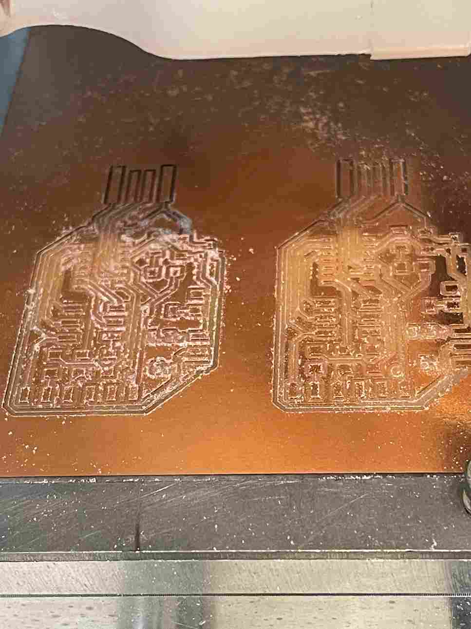
I came back to the lab on a different day hoping to mill a board that I could solder well. Mr. Dubick showed me one of his boards and it was beautiful. All the traces were defined, and any excess copper was milled away. He told me to import 3 bits (adding a 1/64 in flat end mill and changing the PCB engraving bit 0.005” to a 15-degree flute taper stub) at the same time as I did for PCB #2. Since I was using a different bit to do the engraving (1/64 in flat end mill) I had to change the clearance to 2.00 mm. I did this and the board turned out beautiful. I soldered it and plugged it into my computer, but it didn’t work. I tried everything to troubleshoot it but nothing worked so I had to restart again.

PCB #7
- 1/32in flat end mill
- 1/64in flat end mill
- PCB Engraving Bit
Settings
- Trace Depth: 0.20
- Trace Clearance: 2.00 mm
I had to mill another board quick, so I used the same settings as PCB #7. However, when I loaded up the bits, the computer didn’t have the library for the 15-degree flute taper stub so I used a PCB Engraving Bit. This was by no means my best board, but it could work.
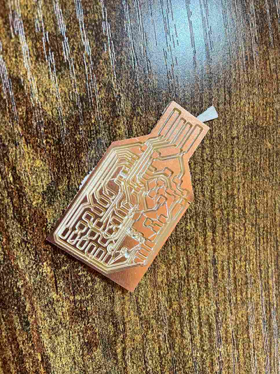
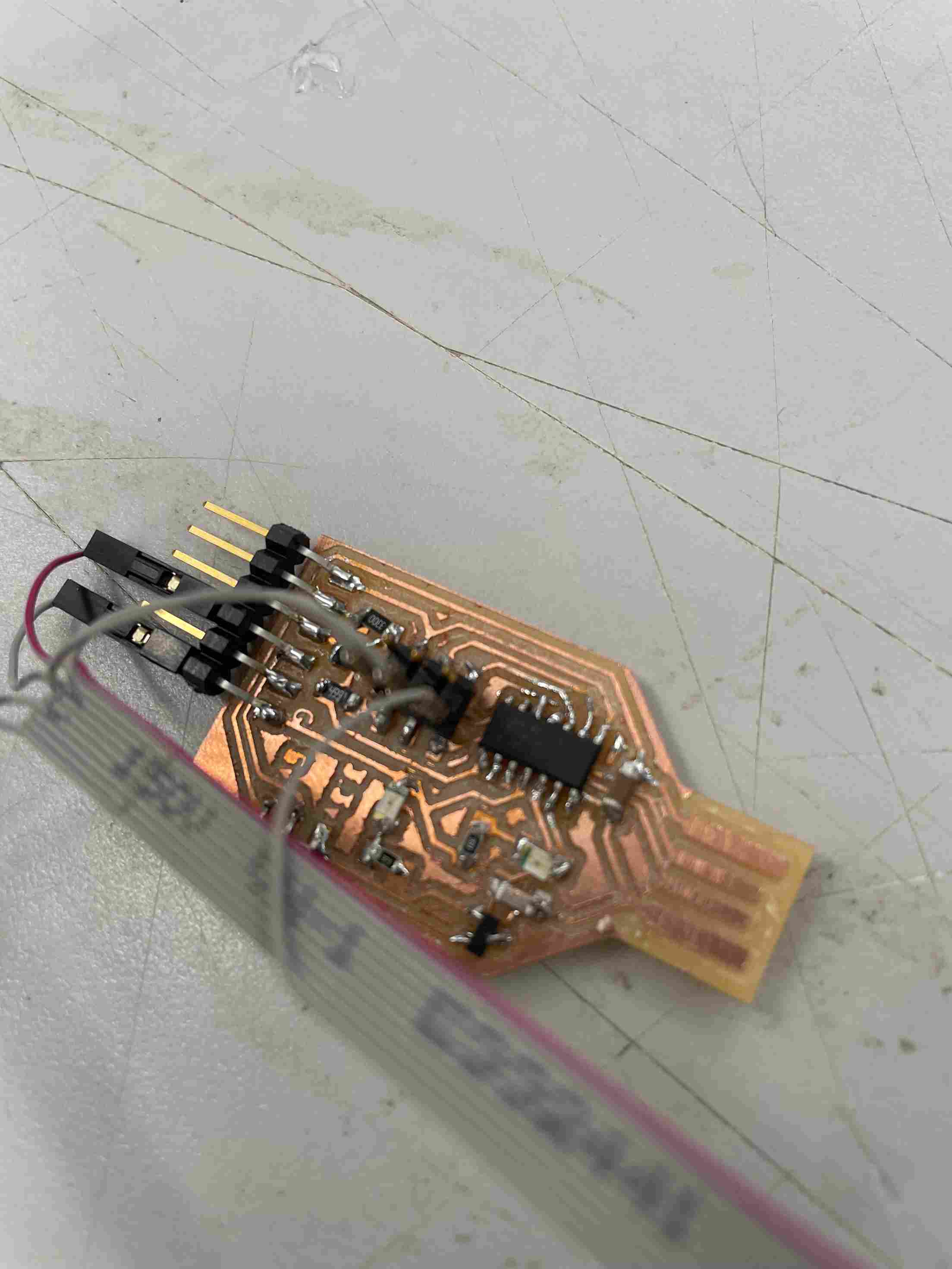
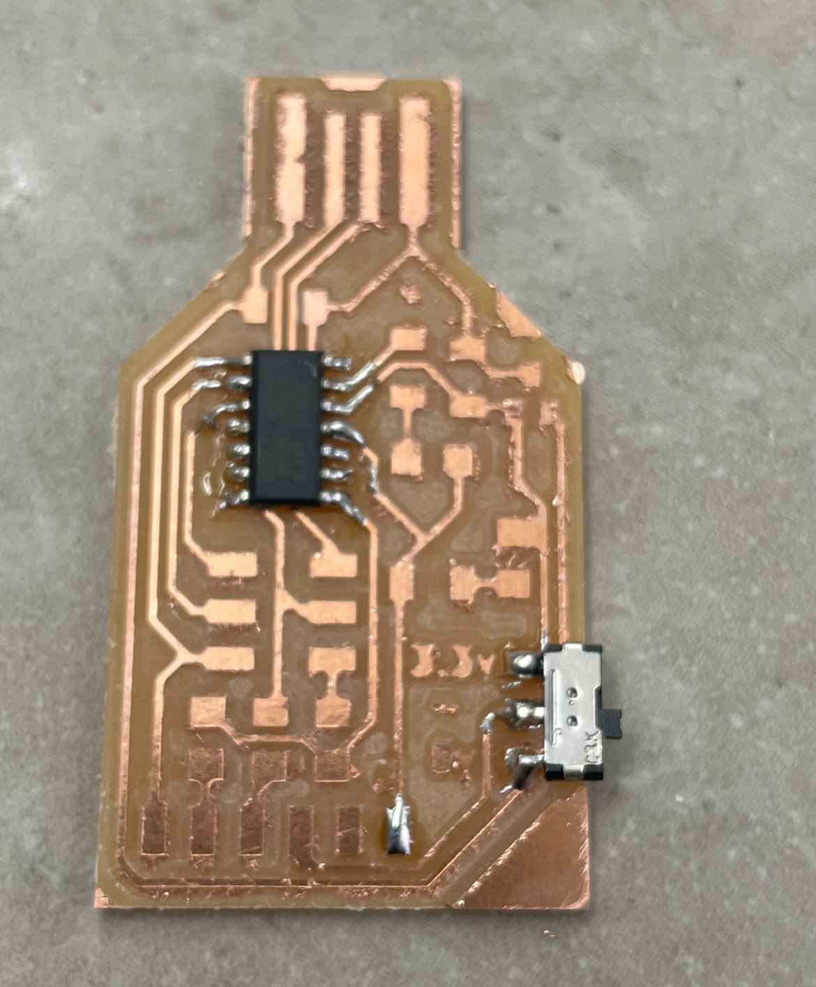
Soldering
I soldered on these components using this image. PCB #6 which was my best board wasn’t working so I had to use PCB #7. After soldering multiple microcontrollers, I was used to this process and my watching this week’s lecture I received some helpful tips on how to solder more efficiently. I plugged it into my computer after shaving the excess copper on the tip (because if I didn’t my computer would short out and the board would be fried) and the LED that indicates power lit up.
After talking with Dr. Taylor, a couple of days later, I realized that I could salvage PCB #2 even if the trace was ripped off by directly soldering the trace to the pin. I did this but realized that the trace that broke wasn’t connected to anything. So, I ended up doing that for nothing. I plugged it into my computer but the light wouldn’t turn on, so the board was useless.
Installing Firmware
I used the atmel ICE programmer mentioned in Dr. Harris’s documentation. Starting from the red wire which was pin-1 (end wire was pin-10) and plugged all the wires indicated on the documentation.
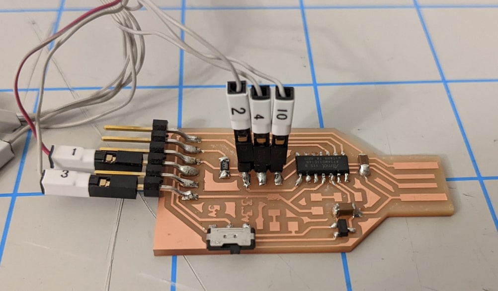
Image from Dr. Harris’s site*
I had to download two firmware’s for the code to process. I learned from a colleague Alaric Pan that the code mentioned in the documentation for the exe file was labeled as windows-r28 but I downloaded windows-r31 so I had to edit this part of the command. I ran the commands in the terminal and my PCB was coded.
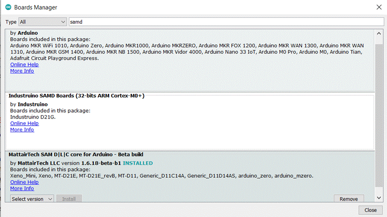
I went into Arduino to test my PCB by uploading a simple LED test code to see if the PCB could be coded. I first had to download the SAMD library by typing this URL https://www.mattairtech.com/software/arduino/package_MattairTech_index.json in preferences
.
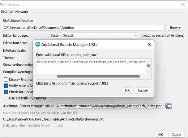
I search for “SAMD” and install the “MattairTech” one only in the board manager.
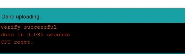
When trying to test the LED on the PCB I ran into a problem. The terminal on Arduino said that my CPU reset and I could no longer plug it in to any port. I tried everything to fix it but the board wouldn’t be recognized by any of the computers in my house so I had to mill another board. I soon realized that this only reset the microcontroller and all I had to do was reprogram it.
My Working Programmer
What is documented below is my working programmer SAMD11C programmer.
Milling
Bit
- 1/32in flat end mill
- 15-degree flute taper stub (but imported a 1/64in)
- PCB Engraving Bit
Settings
- Trace Depth: 0.20
- Trace Clearance: 2.00 mm
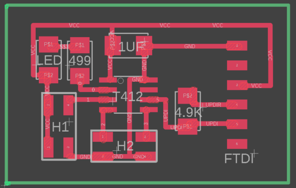
I was having trouble milling any board at this point. I used multiple settings but with help from Mr. Budzukowski he helped me figure out that these settings are the best ones for this kind of board. I also ran into an issue where the outline of the PCB didn’t correlate with the trace cuts. I realized that I had to put the Edge_Cuts file of the board in the outline section of bantam tools. All I had to do was wash the board and scrape off some excess copper. I milled multiple boards just in case something went wrong.
Soldering
My soldering was much improved over this experience. I still used I these components with this image as a reference. The I made sure that the SAMD11C chip was facing the right direction by having the dot on the chip facing the USB entry point.
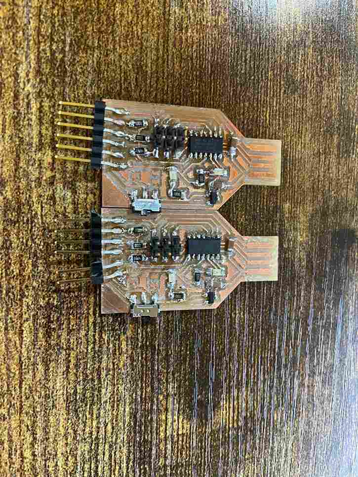
I soldered two boards just in case something went wrong.
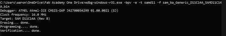
Programming
I performed the same steps mentioned earlier. I used an atmel ICE and connected the pins starting from the red wire which was pin-1 (end wire was pin-10) and plugged all the wires indicated on the documentation. I had to already downloaded the two firmware’s for the code to process. I changed the exe command from windows-r28 to windows-r31. The two firmware’s are in this zip. I pugged the ICE into my computer and provided power to the programmer. I ran this command edbg-windows-r31.exe -bpv -e -t samd11 -f sam_ba_Generic_D11C14A_SAMD11C14A.bin, but I received this error
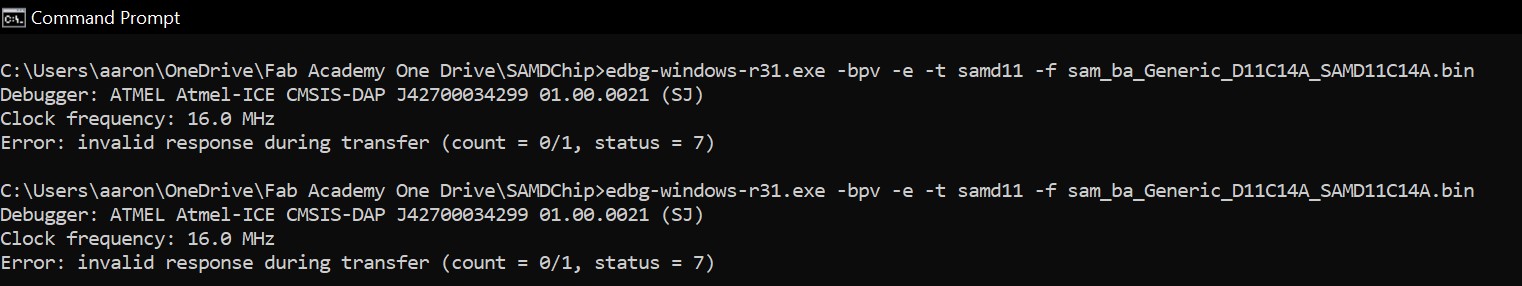
I was again confused, because this wasn’t the first time that I had received this error and other students in the class during this time were receiving the same error. I used both my boards and I knew that they were soldered well so I was confused. I knew that the ICE was working because the previous week it programmed other students’ boards. Dr. Harris had a programmer that could act as an ICE with him at the time and we decided to use that to “jump” the board. He plugged in the wires using this image from his documentation.
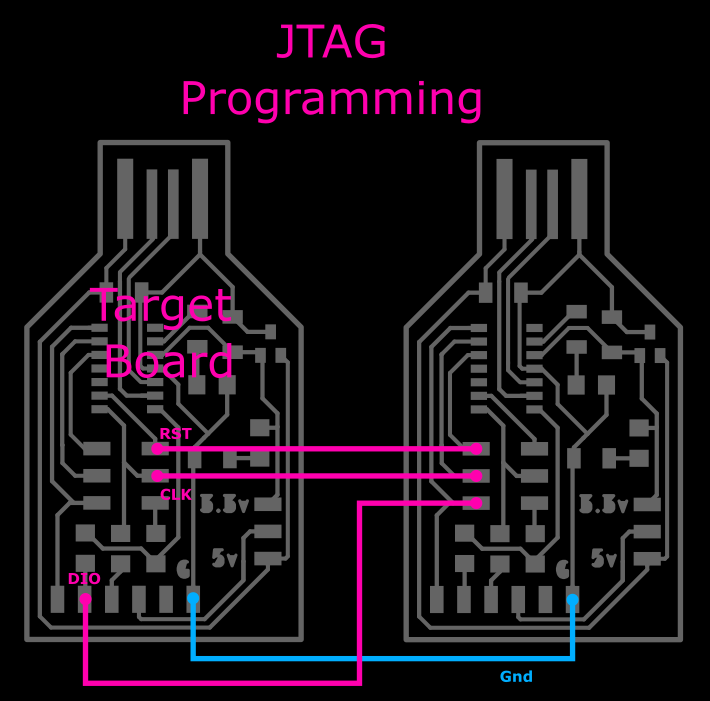
Image from Dr. Harris’s site
He ran the command with his programmer acting as the ICE onto my programmer and it worked, showing this screen.
This means the atmel ICE wasn’t working correctly. Now that my programmer could be read as a USB, Dr. Harris plugged my programmer into his computer to run this code to test the built in LED.
int led = 2;

// the setup routine runs once when you press reset:
void setup() {
  // initialize the digital pin as an output.
  pinMode(led, OUTPUT);
}

void loop() {
  digitalWrite(led, HIGH);   // turn the LED on (HIGH is the voltage level)
  delay(1000);               // wait for a second
  digitalWrite(led, LOW);    // turn the LED off by making the voltage LOW
  delay(1000);               // wait for a second
}
I then received the same error mentioned before and it said my CPU reset, meaning that my programmer couldn’t be read as a USB. I showed this error to Dr. Harris, and he was also confused that my board didn’t work. I initially thought that I fried my USB and my board, that is why I milled another one but when we jumped the board it worked. I checked my tools in Arduino IDE and I realized the problem; the board was a MattairTech Xeno Mini not a Generic D11D14AS. This tool reset the SAMD11C chip on the programmer. I fixed this error and changed the tools to INTERNAL_USB_CALIBRATED_OSCILLATOR. I did this because I wanted the programmer to only act when it is plugged into a USB port.
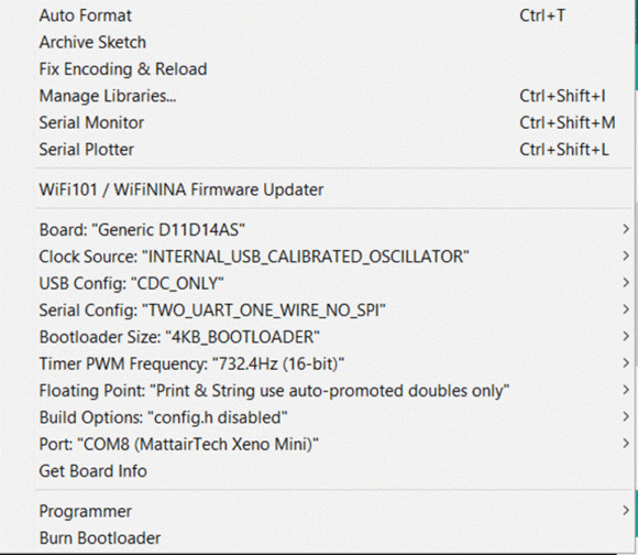
Image from Dr. Harris’s site
After this I ran the code above again and it worked, my programmer LED flashed.
I ran this code below to have the programmer act as a programmer for my blinky board with the ATTiny412 chip.
void setup() {

   SerialUSB.begin(0);
   Serial1.begin(57600, SERIAL_8E2); //Adjust baud rate and use SERIAL_8N1 for regular serial port usage
}

void loop() {
   if (SerialUSB.available()) {
      Serial1.write((char) SerialUSB.read()); //Send stuff from Serial port to USB
   }
   if (Serial1.available()) {
      SerialUSB.write((char) Serial1.read()); //Send stuff from USB to serial port
   }
} //end loop
Connecting to Blinky
Next was to connect my ATTiny412 Blinky to this programmer and program the ATTiny412 to flash the LED. I used these images from Dr. Harris’s documentation to connect to the blinky.

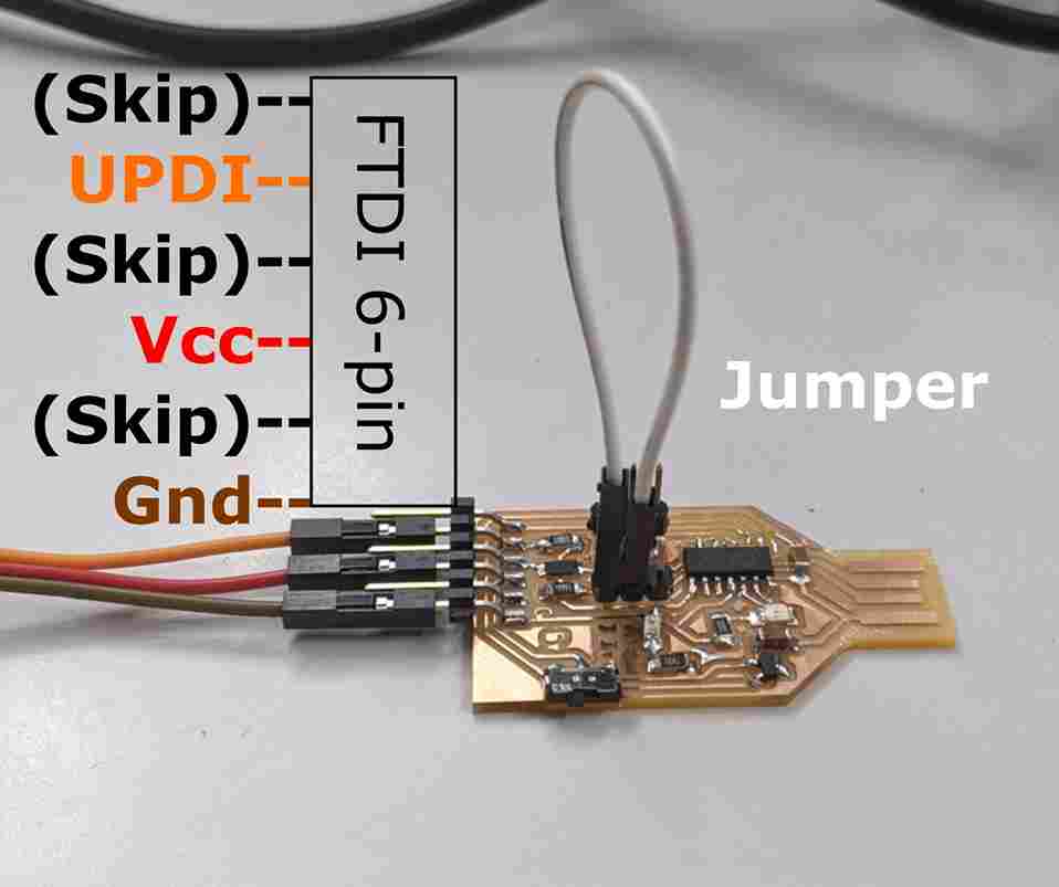
Images above are located on Dr. Harris’s site
I had to connect the UPDI to UPDI, ground to ground, and VCC to VCC. In Arduino IDE I had to configure everything as if I was programming the ATTiny412 chip. This means I had to redownload the library with those chips. I used the settings from earlier on programming the ATTiny412 using an Arduino as the programmer. I plugged in the wires connecting the blinky to the programmer by jumping the two UPDI pins, then connecting the power, ground, and UPDI this image from both the blinky and the programmer.
I loaded up the example code like last time, and it worked
Creating an ICE Programmer
I had my programmer working so I thought I was done, but Dr. Harris gave me a great suggestion: Clean up one of my other new boards (because it wasn’t working) so it can act as an atmel ICE so I will never run into this problem again. I thought it was a great idea and went to work. My first board worked, and I used the same process for the second board. When plugging my second board in the LED flashed, meaning it was receiving power but still didn’t work so I had to clean up the soldering. I viewed it under a microscope and noticed that there was some excess copper creating a short circuit. I cleaned this up but my board still didn’t work. I looked again and saw that there was some cold soldering, so I had to clean that up. I plugged in both Dr. Harris’s working programmer and mine into a USB port. I ran this command free_dap_d11c_mini.bin in the computer with Dr. Harris’s programmer and I had a programmer. The firmware for this is in this zip
Double Sided PCB
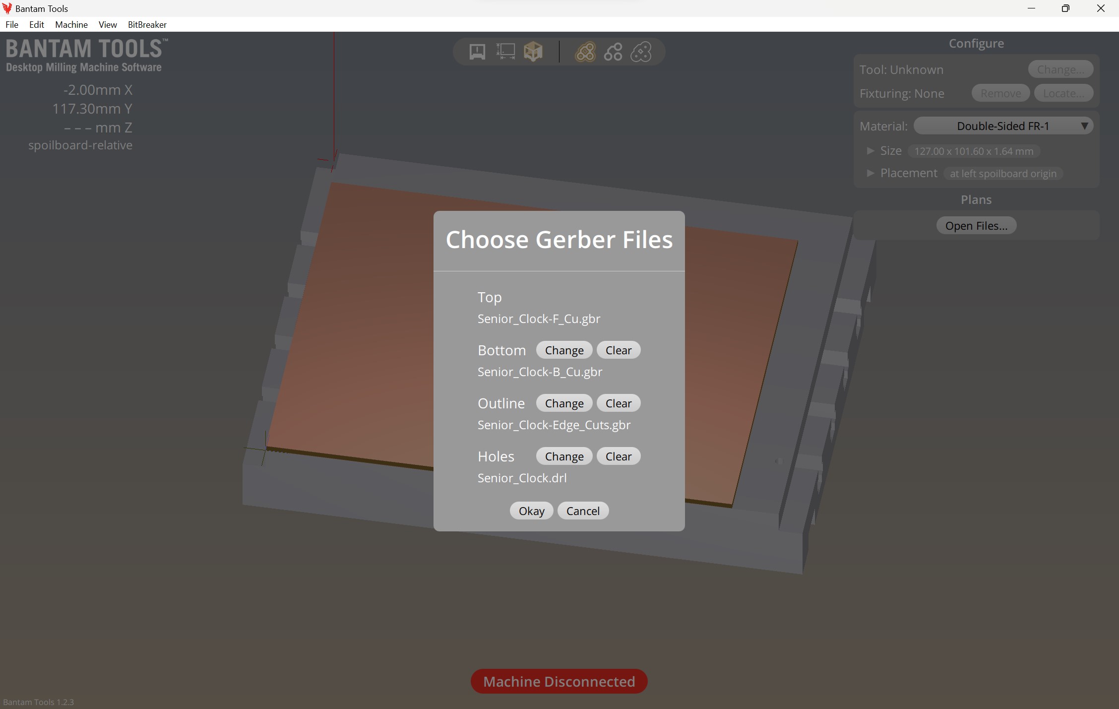
For a double sided PCB uploading the file is a simple process, I looked at Bantam Tools Double Sided PCB Documentation first to get an idea of what to do.
Uploading
To upload the double sided I click did the following Open File > F.Cu
Then I was presented with a loading screen to upload the parameters of the design and I did the following
- Top: F_Cu.gbr
- Bottom: B_Cu.gbr
- Outline: Edge_Cuts.gbr
- Holes: .drl
Bit, Traces and Settings
After that I used the following settings for the traces
Bit
- 1/32in flat end mill
- 1/64in flat end mill
- PCB Engraving Bit
Settings
- Trace Depth: 0.20
- Trace Clearance: 2.00 mm
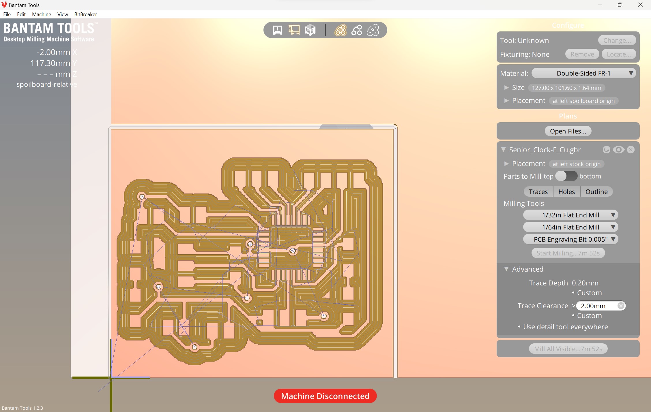
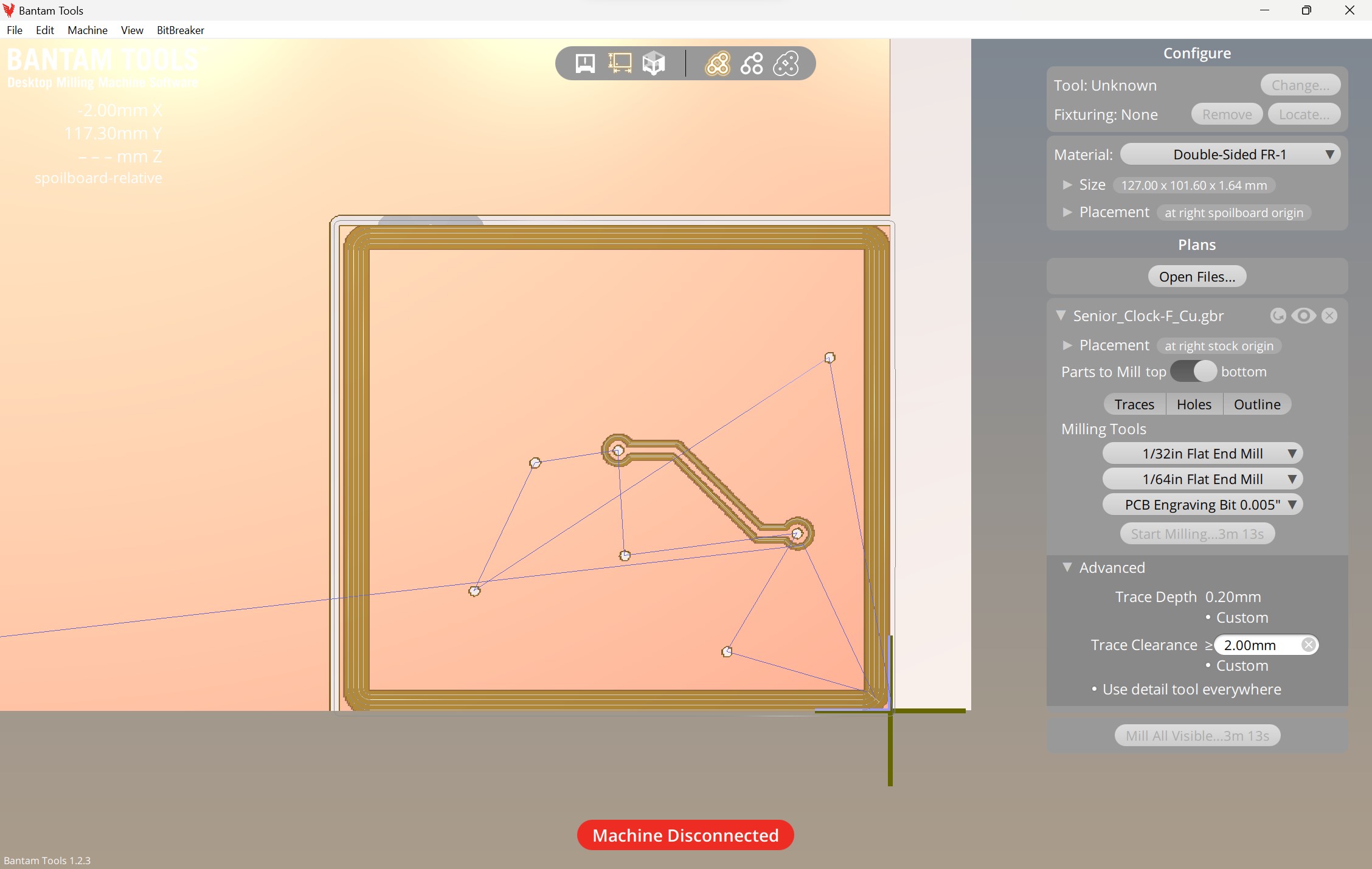
I followed the documentation from bantam mentioned above. I made sure to mill the back side first and not select the outline cut
Group Assignment
Assignment : Characterize the design rules for your in-house PCB production process: document feeds, speeds, plunge rate, depth of cut (traces and outline) and tooling.
For the group assignment, I learned through the group assignment how to properly use the CNC machine and learned exactly what the settings change on the software. The machine we used was a Other Mill Pro. We used bantam software to program the machine. The link to the site is here
Problems I Ran Into
- Ripping traces by having the soldering iron rest on the copper for too long
- Creating solder bridges between different components by adding too much solder
- Soldering the wrong resistors
- Not using the best bits to mill a good board
- Excess copper creating short circuits, so I received error
- The atmel ICE wasn’t working correctly (So I assumed my board wasn’t working when I received an error)
- Importing the wrong tools when uploading code in Arduino IDE
What I learned
I learned a lot throughout this process. The blinky board was relatively easy to make, but the programmer was where I struggled and learned the most. I learned how each bit works in terms of milling traces, like how some bits increase in cut width the deeper they go. I milled at least 10 programmer boards and I learned a lot for each one. Also, for each board I milled, I learned something new for soldering. My first programmer board took me 30 minutes to solder. Now I can solder that board in 5 minutes. I conceptually understood what I was doing when it came to the programming aspect. At first I was just running code and hoped it worked, now I understood why it didn’t work.
Firmware and File Download
- My coding files are available here
- The firmware’s I mentioned earlier are located here Note, this is only for windows because of the .EXE file
- Jtagupdi zip for arduino updi programmer. Extact zip before using.
- The blinky and programmer milling files are located here
To upload the programmer file into Bantam tools I needed to upload the F_cut.glt when selecting open file. Then I had to select Edge_Cuts.gm1 as the outline cut before clicking OK when uploading.