7. Electronics Design
Assignment redraw an echo hello-world board, add (at least) a button and LED (with current-limiting resistor) check the design rules, make it, and test that it can communicate extra credit: simulate its operation
Downloading KiCad
I went to the KiCad website and downloaded the worldwide OSDN versio for windows. To get more familiar with the software I watched tutorial videos provided by Tech Explorations
Single Sided PCB in KiCad
My plan was to create a board with a button that didn’t act as a kill switch but as an input. The plan was for the LED to stay on unless the button was pushed.
Idea
I used my earlier documentation on my blinky board as a reference for this. Except this week I was tasked to add a button. The button couldn’t act as a kill switch but as an input for the ATTiny412. The components I would use from the previous board would be:
- ATTiny412
- 4 Pin Button
- LED
- 330 Ohm Resistor
- 3 Pin Header
- 1 UF Capacitor
KiCad Schematic Editor
I first had to download the component library for Fab Academy first. I used this GitLab link to download the library. Once I downloaded the zip, I extracted the files and loaded it into a separate directory. To incorporate it into KiCad. I performed the following steps:
- Preferences > Symbol Library > Select fab.kicad_sym. This uploaded the symbols
- Preferences > Manage Footprint Library > Select the directory labled fab.pretty
- Preferences > Configure path > Select directory where the files are downloaded
- Don’t change the nickname of the file
I then started adding the symbols into the schematic editor. Most of the symbols already came with footprints. I added the following, most of the component are from the Fab library
- ATTiny412 chip
- Unpolarized Capacitor
- Normal Resistor
- LED
- Male Connector
- 4 Pin Button
I connected these components together. Important things to note, the power and ground had to go from the header to the capacitor then to the microcontroller. This helps the microcontroller not reset if there is a dip in power. I then drew another wire from the power wire into the LED then into the resistor then into the pin. For the button, I had to connect one wire to the ground and the other end to the ground. The last step was the UPDI, and I had one wire go directly from the pin to the UPDI pin. The next step was to edit the microcontroller symbol so I wouldn’t receive any errors after the ERC. I did this by
For pins
- Select on the pin to
- Electrical type: Unconnected
- Select Invisible
For the Power and Ground
- Electrical type power input
Save and close
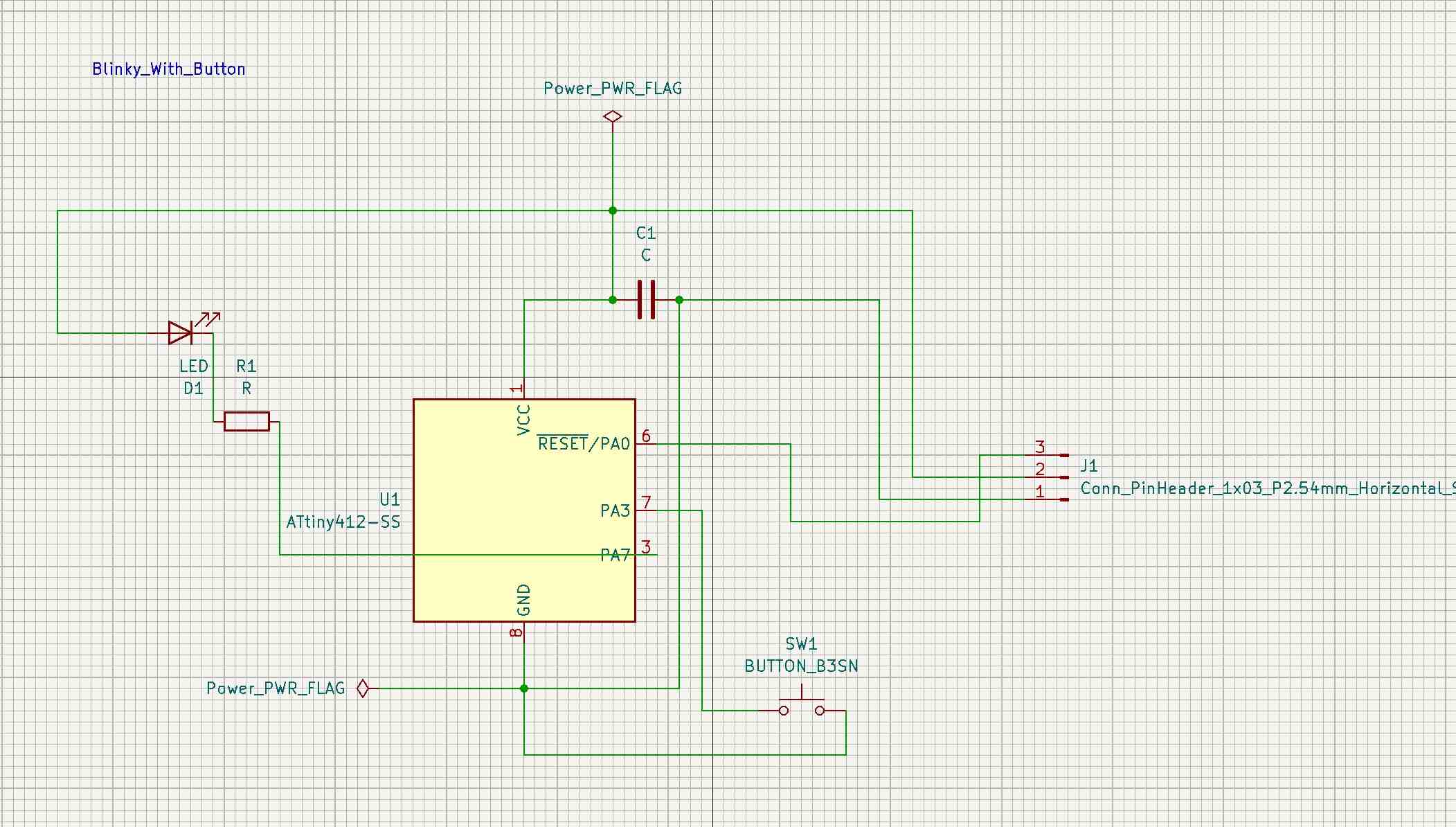
The microcontroller should save the edit but to make sure, I ran the ERC but there was still one error regarding the power and ground. This occurred because the ERC couldn’t find a power source such as a battery. Mr. Dubick informed us that we had to add power flags to the vcc and ground to correct this error. I saved this schematic and uploaded it into the PCB editor.
KiCad PCB Editor
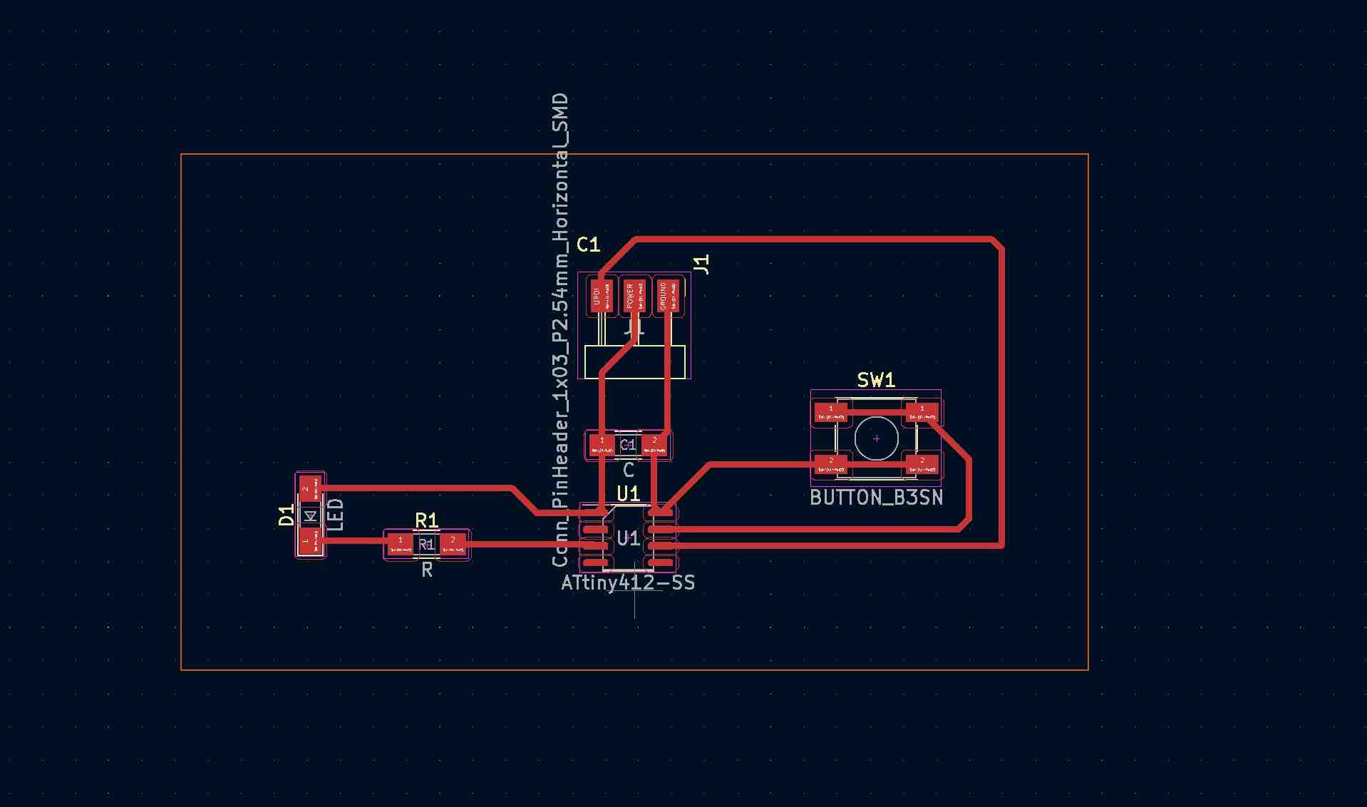
This process was simple but was difficult. I simply had to connect wires to the different components. The difficulties I experienced were placing the components in the right area and not having the wires overlap or be too close together. To help me through this I created constraints for the tracks by performing the following
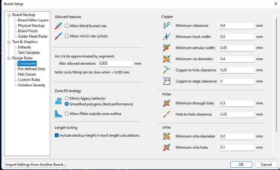
File > board setup > design rules > constraints and I made minimum clearance 0.4 mm and the minimum track width 0.5 mm
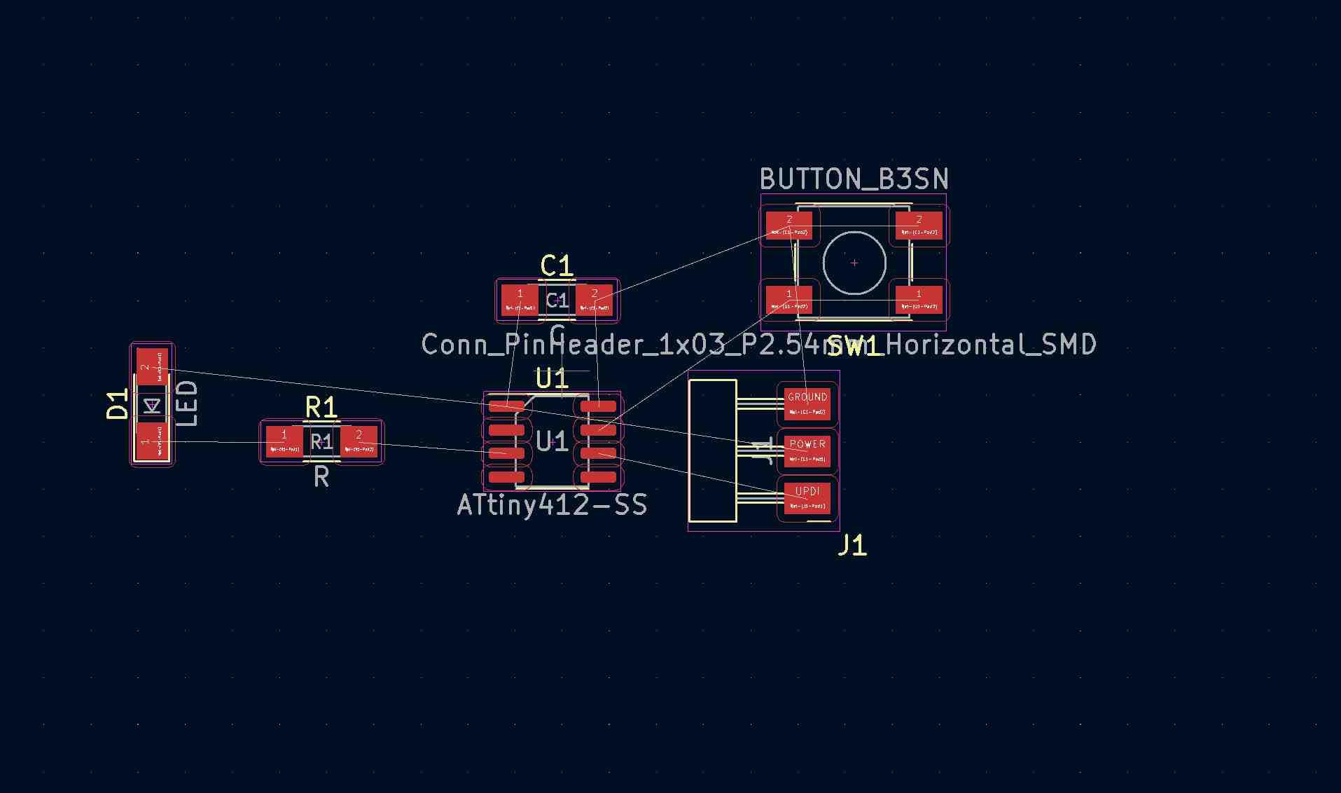
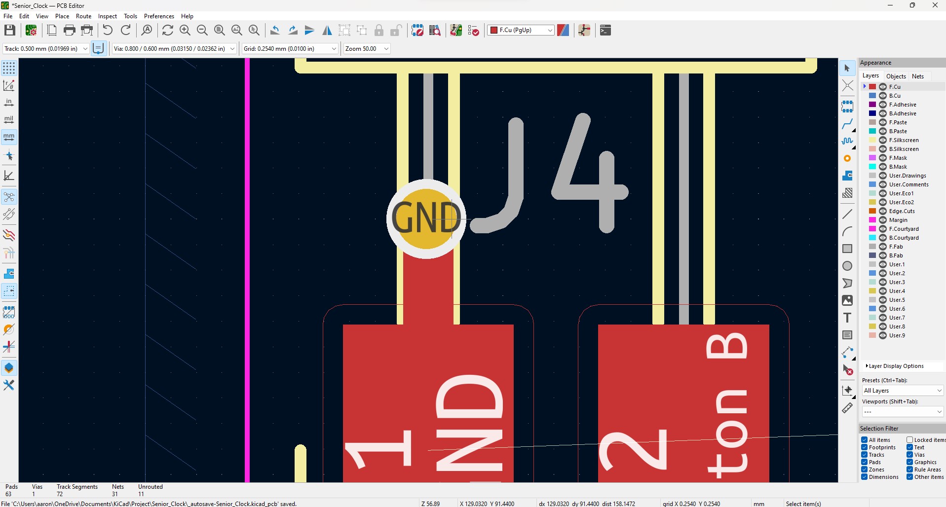
At multiple points throughout the process, I had to change the pin of the button so that it wouldn’t cross over any wires. I went through multiple designs, but I was able to figure out one that worked. One crucial thing that I did was label the power, ground and UPDI pins on the microcontroller and the pins. This made it much easier to connect the right pins.
To check that my design was good I selected the ERC and the only errors I received were silkscreen errors which were nothing to work about.
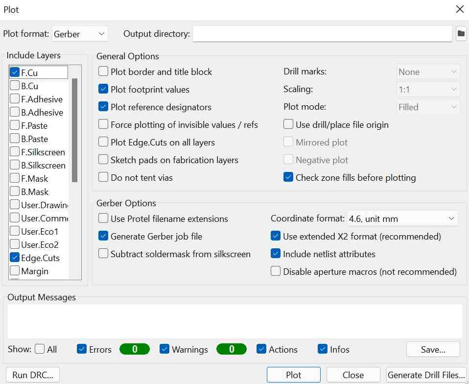
Exporting
I checked that the PCB was ready to export by
- Making sure all of the components were on the F.Cu or the front copper layer
- Creating a box around my PCB on the Edge.Cuts layer.
- Check the 3D Viewer
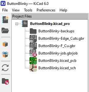
To export the file I had to select File > Plot > Select the layers to plot (Usually the F.Cu and Edge. Cuts) > Plot.
The files showed up in the directory where I saved the schematic and the pcb design.
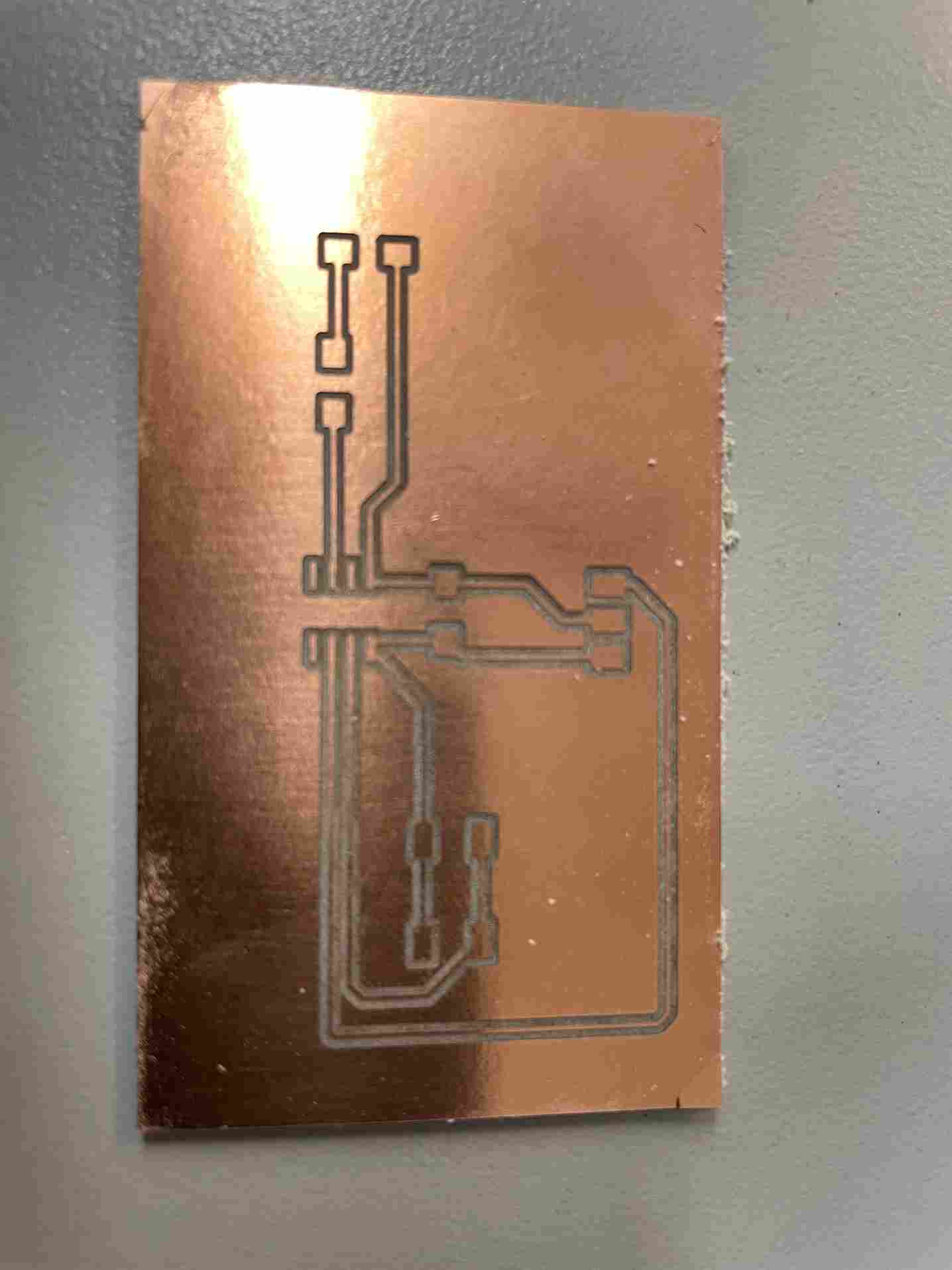
Milling
I uploaded the files into bantam tools milled out the board using my earlier documentation to mill the board. Once I hit mill all visable my board was complete.
Coding
I used example code from Graham Smith’s documentation. I wanted the LED to stay on constantly but only turn off when I pressed the button. I made the pin the button was connected act as a pull up resistor. I then made the pin that the LED was connected to stay LOW (so the LED would turn on) unless the pin that the button was connected to receive a LOW signal (the button is pressed) which would make the LED pin run high (or stop the flow of power). I edited the pin numbers but an error I received was that the code couldn’t run with an ATTiny412 chip.
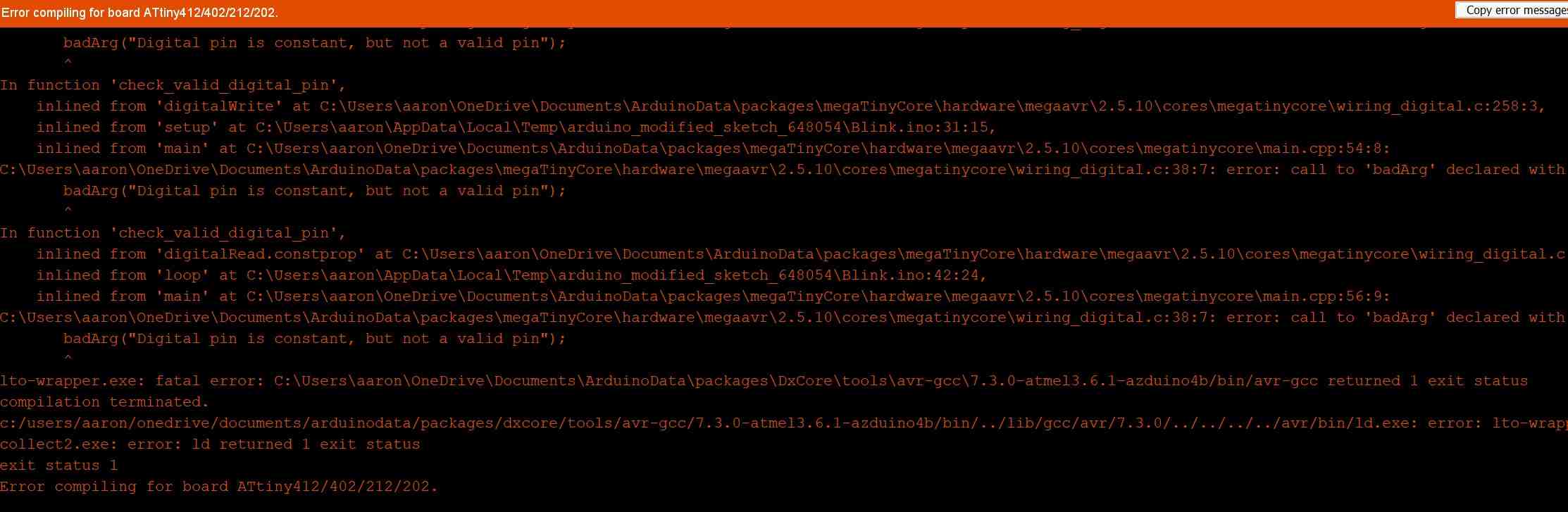
I realized that the error was because my pins were wrong. In the code I had defined a pin as “7” but when looking at the pinout of the microcontroller, pin 7 doesn’t exists, it’s only a label. The real pin was pin 4. I changed this and the code compressed.
Here is the code
int ledPin = 1;

void setup()
{
    pinMode(ledPin, OUTPUT);  // Defines the LED pin
    pinMode(4, INPUT_PULLUP); // Makes the button pin read as HIGH if button isn't pushed
}

void loop()
{
    if (digitalRead(4) == HIGH) // Button Isn't Pushed
    {
        digitalWrite(ledPin, LOW); // LED will stay on
    }
    else
    {
        digitalWrite(ledPin, HIGH); // LED turns off
    }
}
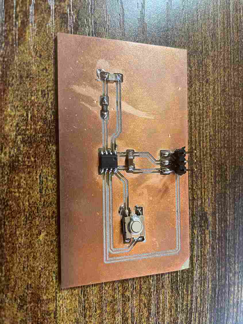
I plugged in my programmer into the PCB, connecting the power, ground, and UPDI. I configured the tools in arduino using my earlier documentation on the ATTiny412 blinky. I ran the code and my board worked.
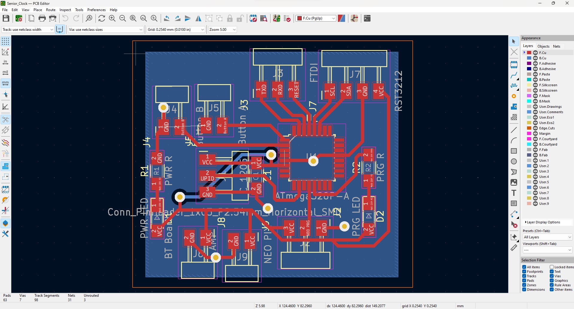
Double Sided PCB in KiCad
This board is based off of a future project. A 7-Segment digital clock that encoporates two bluetooth speakers. Something for my senior year before I graduate from Charlotte Latin. The code I was using was built for an Arduino so I used an AtMega328P for my chip. My materials list is below
- AtMega328P
- Red LED 2x
- 330 Ohm Resistor 2x
- 1 uF Capacitor
- 2 Pin Header 4x
- 3 Pin Header 3x
- 4 Pin Header
KiCad Schematic Editor
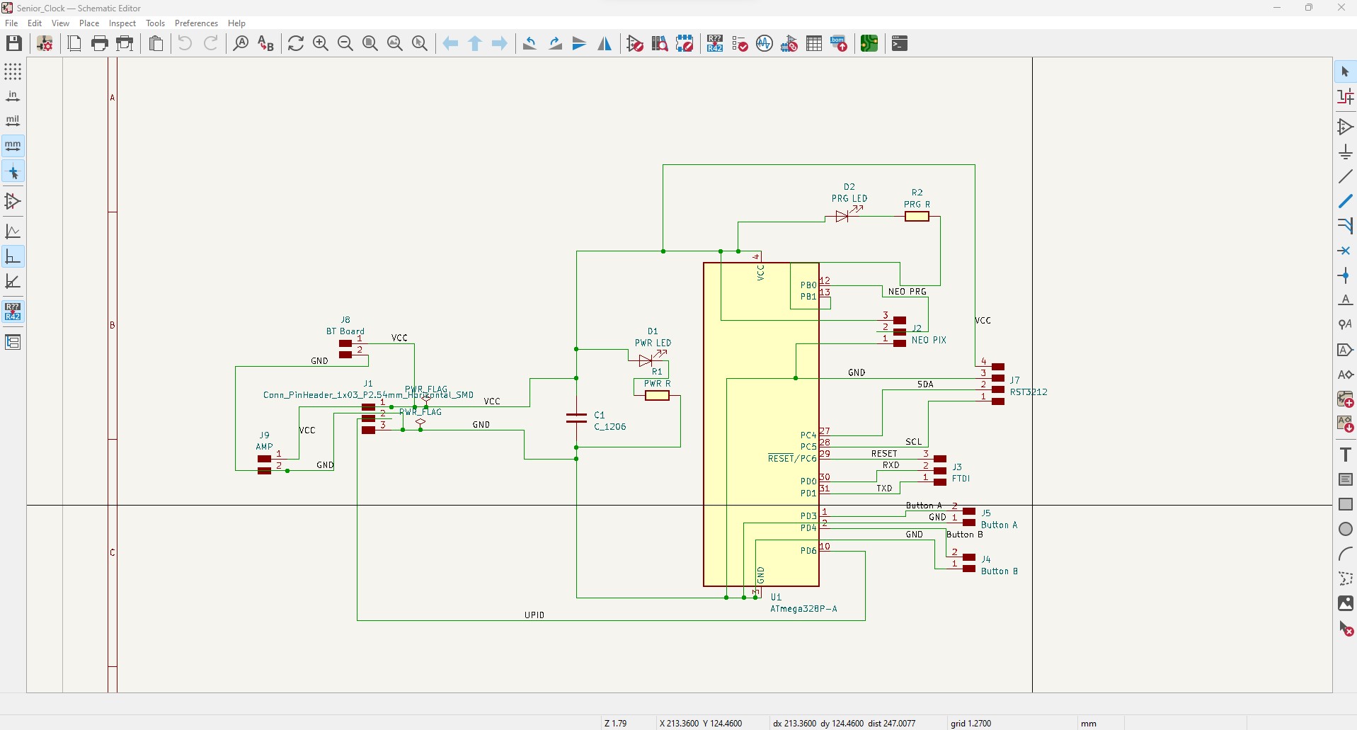
My goal for this board was to have everything run through it, PWR, GND, Data, and PGR. With this in mind I decided that each component should have their respective PWR and GND headers, and not just having ground headers and power headers connected creating a wire mess. I realized this while finishing my final project.
Following similar steps to my single sided PCB documentation above, I created a power LED indicator and I also create a small programming LED so I can test some simple code. Then I added the capacitor and connected that to the main PWR, GND, and UPDI line. Finally I connected all of the pins and to their repsective component headers whether it was I2C or FTDI or the Neopixels I was using. For a double sided PCBs the schematic editor doesn’t really change, its just most of the planning that goes into the design.
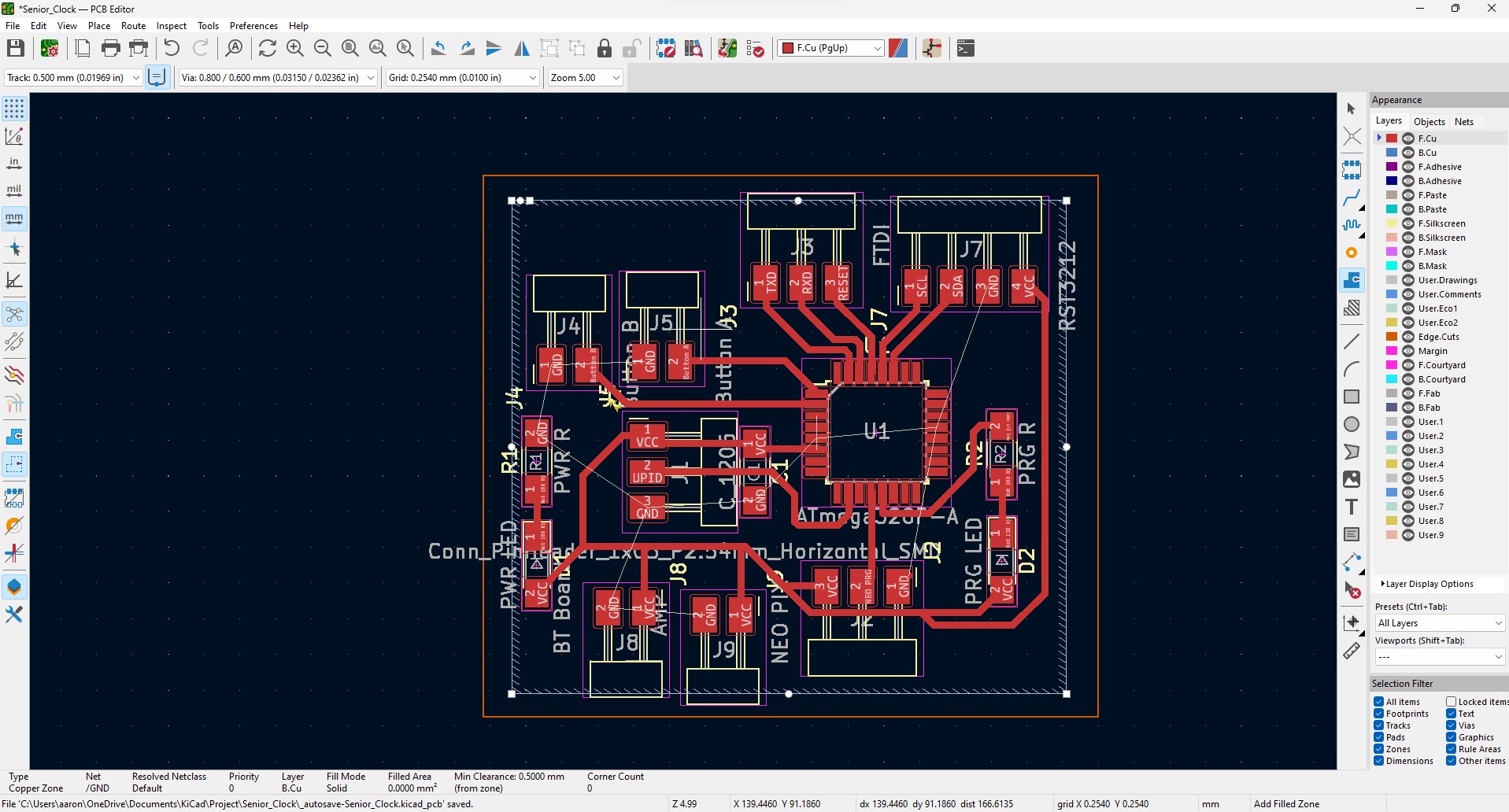
KiCad PCB Editor
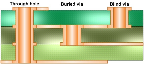
This is where I had to do some research on double sided PCBs with KiCad. I learned that to make a double sided PCB I needed a Via or a connector between layers of a PCB since my PCB was only two layers I could simply use a through hole via I used this image below on figuring out which type of Via I needed
Next I had to figue out exactly how to encoporate this into KiCad. To figure that out, I went to Youtube and found a couple of useful videos. The first one is from Aalto Fablab and the second is from Phil’s Lab. I recommend watching both videos fully as they are very helpful. Aalto Fablab’s video explains how to encoporate a Via into KiCad. Phil’s video goes into more depth about adding a copper pour, a large area of copper that can act as a ground plane in some cases, skip to 1:27:25 to see him add the Vias. I was confused initially about copper pours so I used this link to help explain it along with this image.
Here are the videos I mentioned earlier
Copper Pour
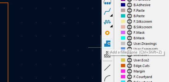
For my PCB I needed a copper pour and one trace on the back of the PCB. For the pour I followed the steps in the video above. First I clicked Add filled zone and then proceeded to click on a starting point to trace the whole outline.
After that I was brought up with copper zone properties. I made sure to select GND as the traces and B.Cu
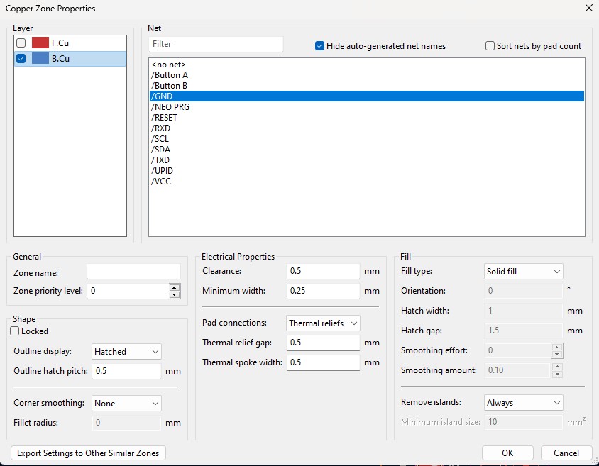
Then I traced an outline of the whole design.
Once I was finished with that I pressed “B” to fill the zone and I was finished with the copper pour.

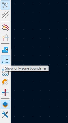
This got pretty annoying to design around so I clicked Show only zone boundaries to hide the filled zone
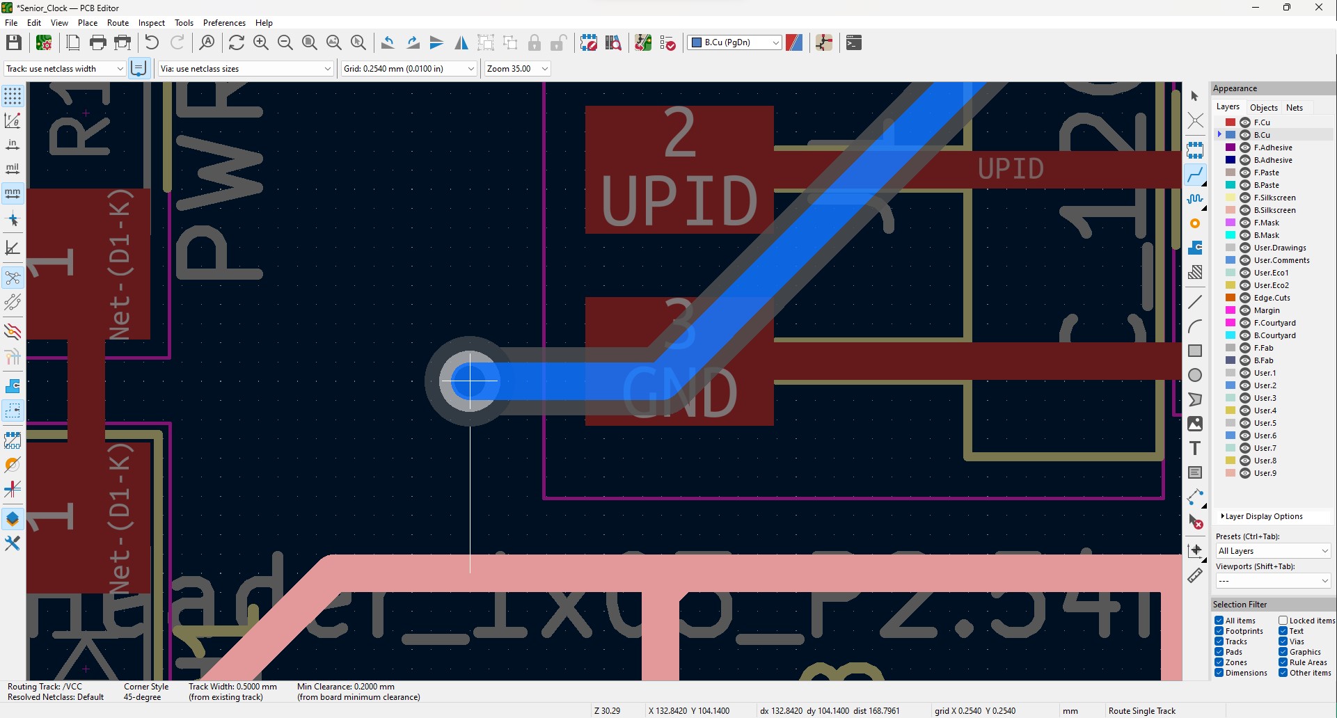
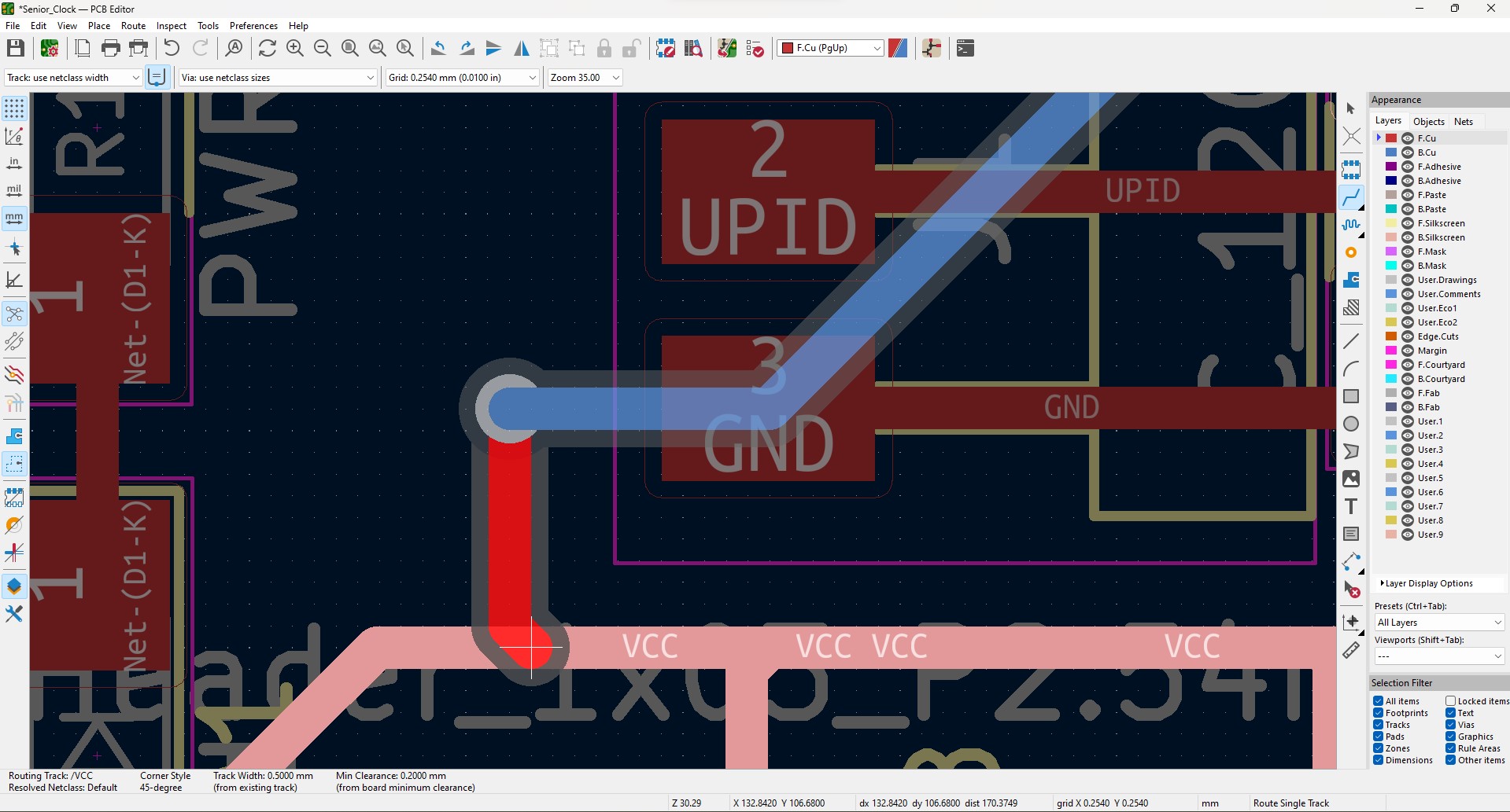
Adding Vias
The next thing I had to do was connect all of the ground pins to the back zone using a via. First I clicked on a trace on the F.Cu like normal then rooted a small trace outward, then I pressed “V” to insert a via. With the via connected I double clicked it and the via was set.
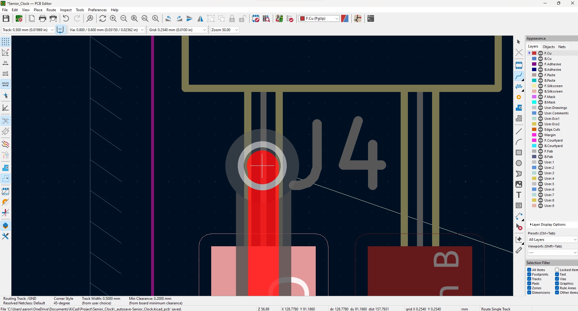
I had to make sure that the via settings were correct with the ones we had in the lab so I double clicked on the via to make sure I had the right settings. The via hole is the actual size of the rivet and I’m using .8 mm rivets. The via diameter should be twice the size of the via hole.
- Via Hole: 0.8 mm
- Via Diameter: 1.6 mm
Next I had to connect a VCC trace to another side of the board using a via so similar to the steps above I rooted a trace then added a via, but this time instead of double clicking I created a trace on the B.Cu then moved it toward its intended location.
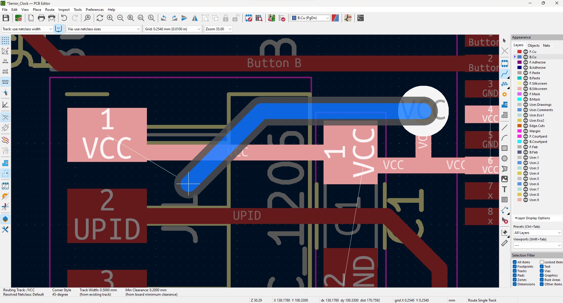
Then I added another via to bring me back to the F.Cu then connected that trace to its intended area.
IMPORTANT
Since I added a pour earlier I had press “B” to fill the zone again but this time with the new trace I created on the back layer. If I didn’t do this, then the trace wouldn’t show up on the B.Cu and it would just be the vias.
Exporting
Similar to the documentation for the single sidded PCB I ran the DRC and everything checked out ok. Then I hit Plot and I checked the following
- F.Cu
- B.Cu
- Edge.Cuts
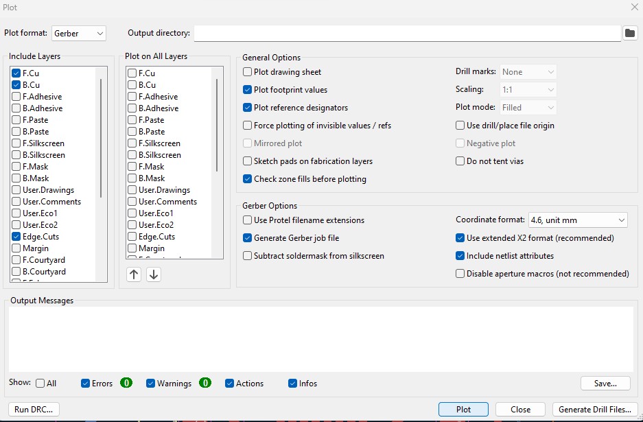
After that I clicked plot
Since I had vias I had to also click generate drill files on the same menu. After clicking that I made sure to check the following
- PTH and NPTH in single file
- Drill Units: Millimeters
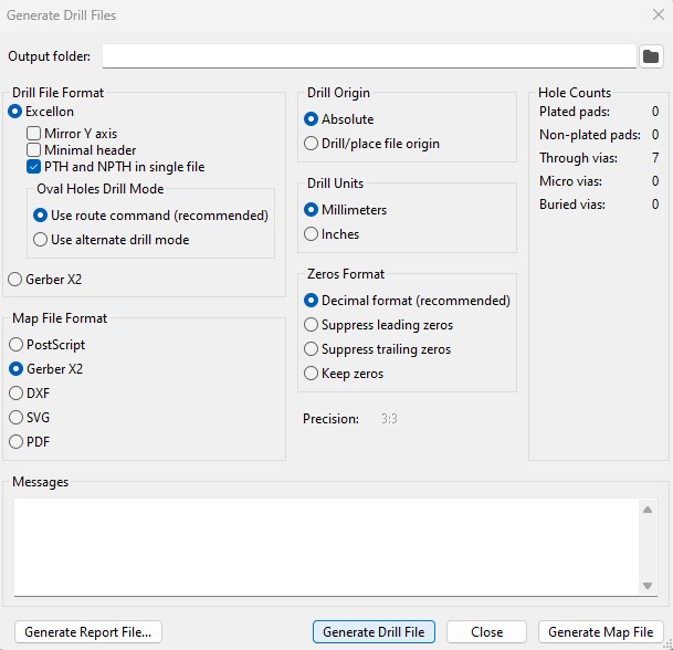
Then I hit generate drill files. I saw a .drl file in the project directory and I was done exporting.
Milling
For this step I used my PCB Production documentation on double sided PCBs and after that I was done with designing aspect of the PCB.
Problems I Ran Into
- Finding the correct symbols with footprints
- Creating constraints
- Wiring the PCB so the wires don’t cross
- Editing the pins on the microcontroller so the wiring in the PCB editor wouldn’t cross over.
What I learned
This week I learned a lot about pull up and pull-down resistors. The microcontroller that we use ATTiny412 has a built-in resistor that when called upon can act as a pull up resistor. Because of this I didn’t have to include a resistor in our designs. I also learned that adding symbols in the schematic editor doesn’t really correlate to anything unless it has a footprint assigned to it. The importance of having the correct wires connected in the schematic editor is critical for the PCB editor. This is because the PCB editor won’t allow you to connect any wires unless they are connected in the schematic editor. In the PCB editor it doesn’t tell you how to connect the wires, but where. Because of this I almost connected my power pin directly into the microcontroller and then into the capacitor (which would make the capacitor useless). I realized this and was careful that the wires were connected as intended in the schematic editor
Group Assignment
The group assignment this week was to learn how to operate an oscilloscope and a multimeter. I have used a multimeter before, so the equipment was very familiar, but the oscilloscope was new to me. We were able to judge the analog signal of the LED in the programmers. Unlike a multimeter, which provides an average value when using, an oscilloscope provides real-time adjustments to the LED. The site is located here.