Week 7. Electronics Design (Mar 1)
Week 07 Assignment
-
redraw an echo hello-world board,
-
add (at least) a button and LED (with current-limiting resistor)
-
check the design rules, make it, and test that it can communicate
-
extra credit: simulate its operation
KiCAD Preparation
Prior to starting Fab Academy, our instructor Mr. Dubick, gave us our personal access codes to KiCAD Like a Pro, and advised us to complete lessons 4 and 5 before starting this week, which talked about going through a full process of designing a PCB. KiCAD Like a Pro 3e is an online textbook created by Tech Explorations that helps us learn how to design PCBs with KiCAD, the main electronics designing software our lab uses.
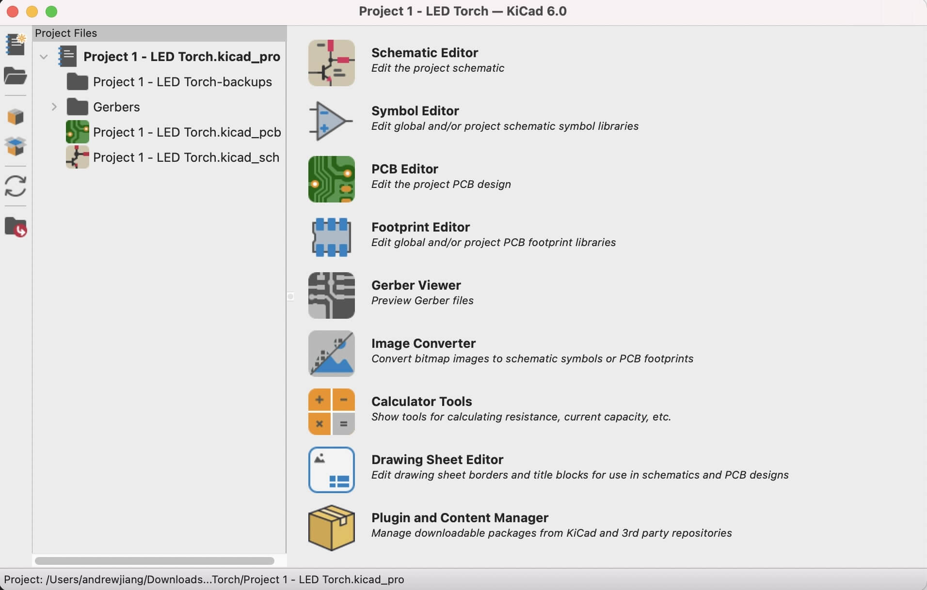
Following Mr. Dubick’s advice, I decided to do the tutorials for lessons 4 and 5, which walked me through creating a simple LED torch PCB. The process for creating the PCB can be split up into two main parts: designing the schematic in Eeschema, and designing the PCB in PCB editor.
First, I had to create an schematic that would essentially act as a map of the electrical connections and components. While I have seen electronic schematics before in engineering classes and could recognize some of the symbols, I’ve never actually created my own one from scratch before. Thus, I got to learn this skill while following along with the videos. These are the steps I followed for the first part of the process.
As you can see, the steps were simply 1. Create and setup the new file 2. Add the symbols for the components I was using 3. Annotate the symbols to give them a label and assign footprints (actual representations of the component) to each component 4. Use wires to connect the components together 5. Add nets (labelling wires for convenience) 6. Perform and pass an ERC (Electrical Rules Check) to make sure there are no errors
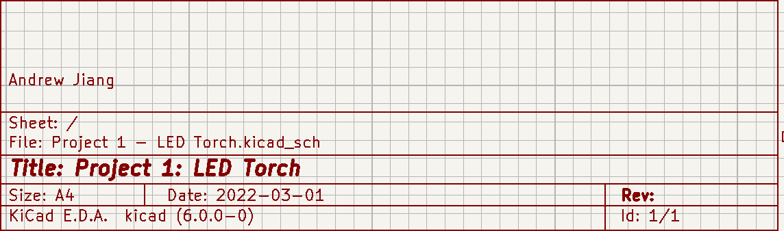
To start, I created a new project in KiCAD and opened up Eeschema Schematic Editor, which is a software that I use to design my schematics. Then I went to the bottom right corner to the schematic info and modified it, resulting in this.
Then I added the symbols for the components for the LED Torch, which were a single switch, a single battery pack, an LED, and a resistor. I did this by going to the right sidebar and clicking the third button down from the top, which brings up a library of imported symbols. Then I searched up each component that I wanted, and placed it in a relatively reasonable orientation. Here is an example of some of the notable symbols
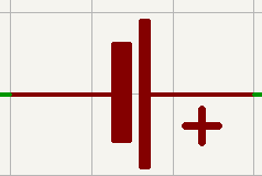
That’s the symbol for a battery pack, with clear labels on the positive and negative sides, and it’s one short and one long lines indicate that it only has one cell.
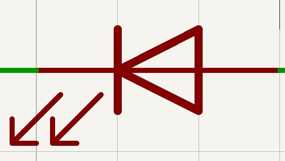
This is the symbol for an LED, and you can clearly see the anode (positive) and cathode (negative) based on the fact that the triangle always points in the direction of the cathode.
The next steps were to annotate the symbols and assign footprints to them. I did this by clicking the button with a R?? -> R42 that was to the left of the electrical rules check symbol in the top toolbar that looked like this. Once I clicked it, it brought up a popup which gave me the option to annotate. I clicked that, and the popup said something like this
Assigned D? to D1
Assigned R? to R1
Assigned BT? to BT1
Assigned SW? to SW1
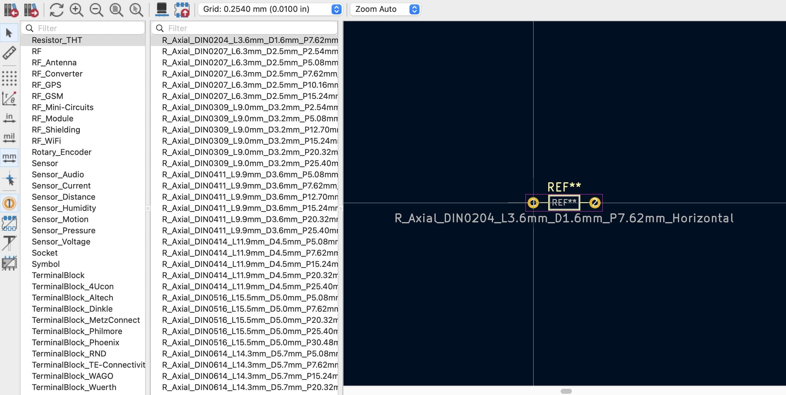
I went back to the schematic and saw that the changes had been made, so next I assigned footprints to each component. For each component, I would click on the symbol itself, bringing up a settings popup. Then I would go to the footprint row of the table, go under value, and click on the little option that brought me to the footprint library. Next I would use the library filter and the search bar to find the corresponding footprint that I wanted, and then make sure the show footprint checkbox was selected.
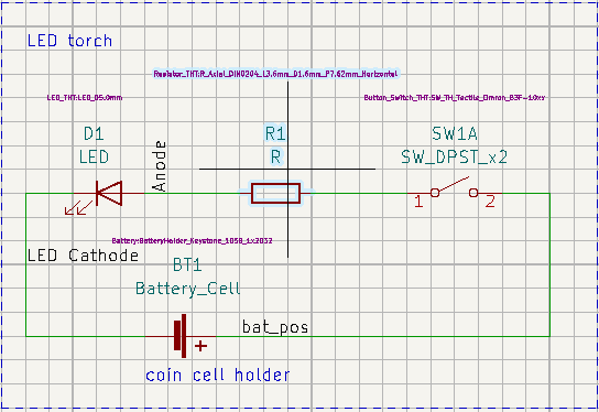
This is the footprint library. After associating and annotating, then I added some wires to connect all the components together. After adding on the wires, I then added nets, which labelled the wires in a convenient manner. This was my finished schematic design for the LED torch.
I performed the Electrical Rules Check and there were no problems. Next I moved to the .pcb file in PCB editor, which started as another empty file.
Here are the steps I followed for the second half of the LED Torch project 1. Import schematic into PCB Editor 2. Draw the edge cuts 3. Add tracks (traces connecting the components) 4. Use silkscreen layer for text and graphics 5. Perform and pass a DRC (design rules check) 6. Export Gerber files
First I went to the top toolbar and clicked on the option that said “Update PCB with changes made to schematic”, which brought in my schematic into PCB editor. I then went to the right side and selected the edge cuts layer, and next I drew the outline for my PCB. After, I took in the schematic components and placed them inside the edge cuts in the F.Cu layer. Finally, I added tracks, tracing each of the components together. My finished LED torch PCB looked like this.
ATtiny412 Echo Hello-World Board
This week, our assignment was to design an echo hello world board, add at least a resistor, button, and LED, and test that the board can work by programming it through the SAMD11C programmer board that we made in week 5: Electronics Production. As you can see, the assignment is very similar to the week 5 assignment with one added step, which is to actually design our own boards instead of using a pre-made design.
This assignment was unique in that I had never really explored designing custom PCBs before this, and thus I had no prior experience with it. With the previous weeks, such as 3D printing, laser cutting, vinyl cutting, etc, I had at least some previous experience with the skill from engineering classes offered at our school. But before Fab Academy, I had never even heard of KiCAD or EagleCAD before. Although I was a bit nervous in the beginning, I ended up learning quite a bit this week and gaining a new skill.

I followed these steps to design, mill, and test my PCB. 1. Desiging a schematic in KiCAD Eeschema 2. Actual PCB design in KiCAD PCB Editor 3. Milling out gerber files using OtherMill CNC 4. Soldering components onto the board 5. Programming using SAMD11C programmer
Learning about Buttons and Pull-Up/Pull-Down Resistors
Before we worked on designing our PCBs, our instructors Dr Harris and Mr Dubick, gave all of our lab’s students a lecture on pull up and pull down resistors, as well as momentary push buttons. Here is the document with my complete notes from that lecture.
Basically there are two kinds of switches, slide switches that have three pins with two pins always connected, and momentary switches that have two pins, and a lever that mechanically connects the circuit.

This is an example of what a slide switch does. In electronics, there are both digital and analog values. For example, the analog values range from 0 to 5V, and the digital values are either a 0 or a 1. But if digital values can only be two values, and analog values can range anywhere from 0 to 5V, then how do we make sure that they match up? We can use a momentary pushbutton, which makes sure that analog values are either 5V or 0, matching up with 1 and 0 of the digital values. Since current generally flows through the path of least resistance, and there is no resistance, just a power and a ground will kill the circuit. Thus we can solve this by either adding a pull up resistor or a pull down resistor.

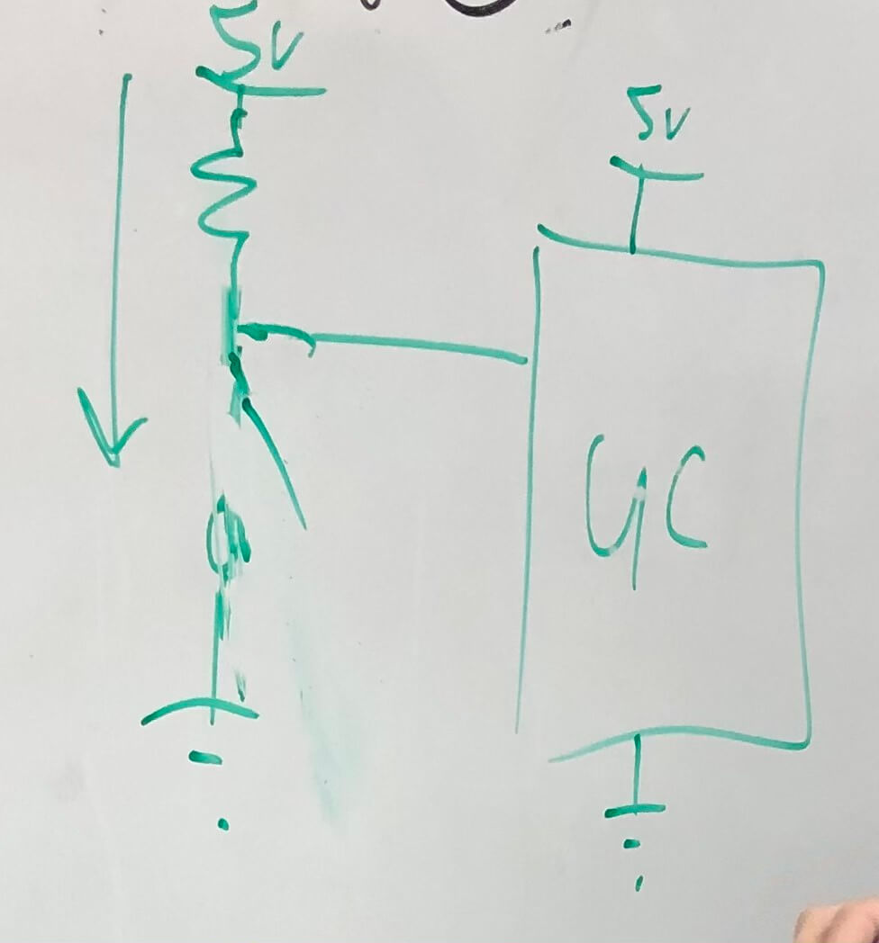
This is what it would look like without a resistor. In concept, a pullup and pulldown resistor are the exact same things, just on opposite sides. A pullup resistor means that the normal analog value is 5V, and a button press would bring the digital value down to 0. An example of this would be if you started a program, and the LED was always on, but when you pressed the button, the LED turned off. This is what a pull up resistor would look like, and as you can see, the resistor is on the power side.
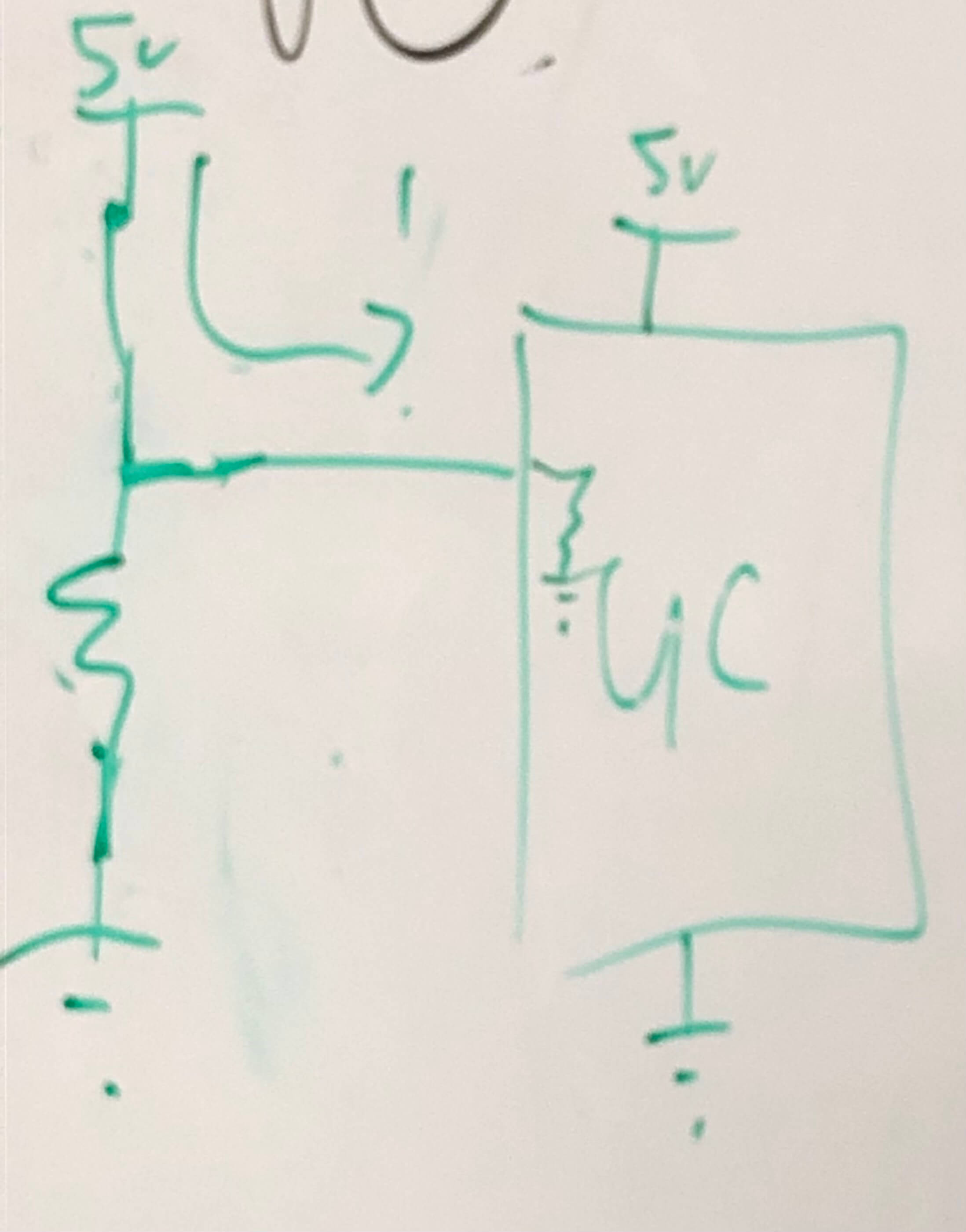
A pull down resistor is essentially the same thing but reversed. Instead, it pulls the normal analog value to 0, and a button press would produce a 1 digital value. For instance, if a button was pressed the LED would turn on, but it would otherwise remain off. This is what a pull down resistor would look like, and as you can see, the resistor is on the ground side.
We know that we need either a pull up or pull down resistor, but we don’t know which resistor to use. In this case, it would depend on the LED we are trying to light up, since different LEDs require different voltages to trigger. We can use ohms law or voltage = current * resistance (V = IR), in order to figure out the wanted resistor. For example if we had a red LED and we wanted 20 milliAmps (mA) of current and 3.8 volts (V) of voltage, simple divide 3.8 / 0.020 = 190 ohms minimum resistance. Of course, we wouldn’t want a resistor too close or too high from 190, as we need to keep in mind that a higher resistance means a dimmer light. Thus we could use around the 330 or 490 range. This is just a hypothetical example, but it shows how this concept is applied, and I used this idea with my hello world board.
To get practice with pull up, pull down, and buttons, our instructors had us follow an Arduino lesson in TinkerCAD, which had us build a practice circuit with a pullup/pulldown resistor. TinkerCAD is a fairly simple yet versatile design tool where you can create CAD drawings and circuits, and thus it is the perfect tool for practicing a new concept without having to get the physical components out.
I went to the TinkerCAD website and created a new circuit design. Then I went to the right sidebar and dragged out these components onto the interface. - Arduino Uno - Breadboard - Pushbutton - LED - Resistor (modified to 330 ohm) Then I wired up the components as seen in this schematic
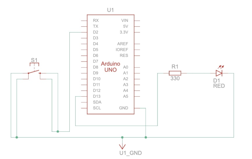
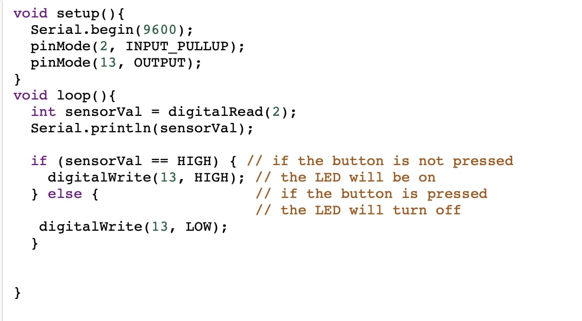
As you can see, I have the pushbutton wired from pin 2 of the Arduino into ground, and the LED and resistor are wired from pin 13 of the Arduino into a shared ground. For the code, I just copied the code from the tutorial, and modified it to include the LED. This is the pull up code I ran for the TinkerCAD example.
This was the result of these tests.
Of course, I could just as easily turn it into a pull down resistor by reversing the HIGH and LOW values in the code. This is what it would look like if I did that.
Although this is only a simple example, it’s still a good demonstration of pull up/pull down resistors and momentary pushbuttons, and I learned a lot from this lecture.
Ideation and Design
For this week’s main PCB designing assignment, I decided to make an echo hello world board based on the example ATTiny412 blinky board made byDr. Harris. The components needed for the blinky board were - 1 ATTiny412 chip - 499 ohm resistor - LED - 1 uF capacitor - 4.9k ohm resistor - 6 pin header - 2 2x2 vertical headers This is what Dr. Harris’s design looked like
However, since I only wanted an MVP (Minimally Viable Product), I decided to simplify the design quite a bit while adding a button. After some thought, I surmised that I would only need these components for my personal hello world board. - 1 ATTiny - 1 Blue LED - 1 1uF capacitor - 1 momentary pushbutton - 1 resistor between 330 - 500 ohms. - 1 3 pin header for ground, power, and UPDI By making only an MVP, not only was I saving components from being used, but I was also saving potential future headaches down the road in programming.
Now that the idea was complete, then came the actual designing in KiCAD. While I am by no means a master a KiCAD, I do have some experience with using it, so this wasn’t as hard as I initially thought. I pretty much followed the same exact steps as the LED torch, just with a little more thought put into positioning and how things would fit on the board. Again here is the full list of steps I took to design the PCB. Eeschema 1. Create and setup the new file 2. Add the symbols for the components I was using 3. Annotate the symbols to give them a label and assign footprints (actual representations of the component) to each component 4. Use wires to connect the components together 5. Add nets (labelling wires for convenience) 6. Perform and pass an ERC (Electrical Rules Check) to make sure there are no errors PCB Editor 1. Import schematic into PCB Editor 2. Draw the edge cuts 3. Add tracks (traces connecting the components) 4. Use silkscreen layer for text and graphics 5. Perform and pass a DRC (design rules check) 6. Export Gerber files
First, I created a new KiCAD file, went into Eeschema, and called it “Electronics Design - Modified ATTiny” since I was modifying Dr. Harris’s design. Then I went to the bottom right corner and modified the sheet info with my name and the title.
Next, I wanted to add the symbols and footprints for the components I was using. To do this, I would have to add in the special Fab library of symbols and footprints into KiCAD. My instructor Mr Dubick shared the Fab electronics component library gitlab page with all of our lab’s students. However, I still had no idea how to actually add the library to KiCAD. Thus, there were two helpful resources I used to learn how to add libraries to KiCAD. First, I went back to the KiCAD Like a Pro 3e textbook, and went to section 9 lecture 8: “how to install symbol libraries in bulk”. Secondly, I went to the read.me file on the Fab electronics component library, which had step by step instructions on how to bring in the Fab library. 1. Clone or download this repository. You may rename the directory to fab. 2. Store it in a safe place such as ~/kicad/libraries or C:/kicad/libraries. 3. Run KiCad or open a KiCad .pro file. 4. Go to “Preferences / Manage Symbol Libraries” and add fab.kicad_sym as symbol library. 5. Go to “Preferences / Manage Footprint Libraries” and add fab.pretty as footprint library. 6. Go to “Preferences / Configure Paths” and add variable named FAB that points to the installation directory of the fab library, such as ~/kicad/libraries/fab or C:/kicad/libraries/fab.
After following these six instructions, this is what the fab library looked like.
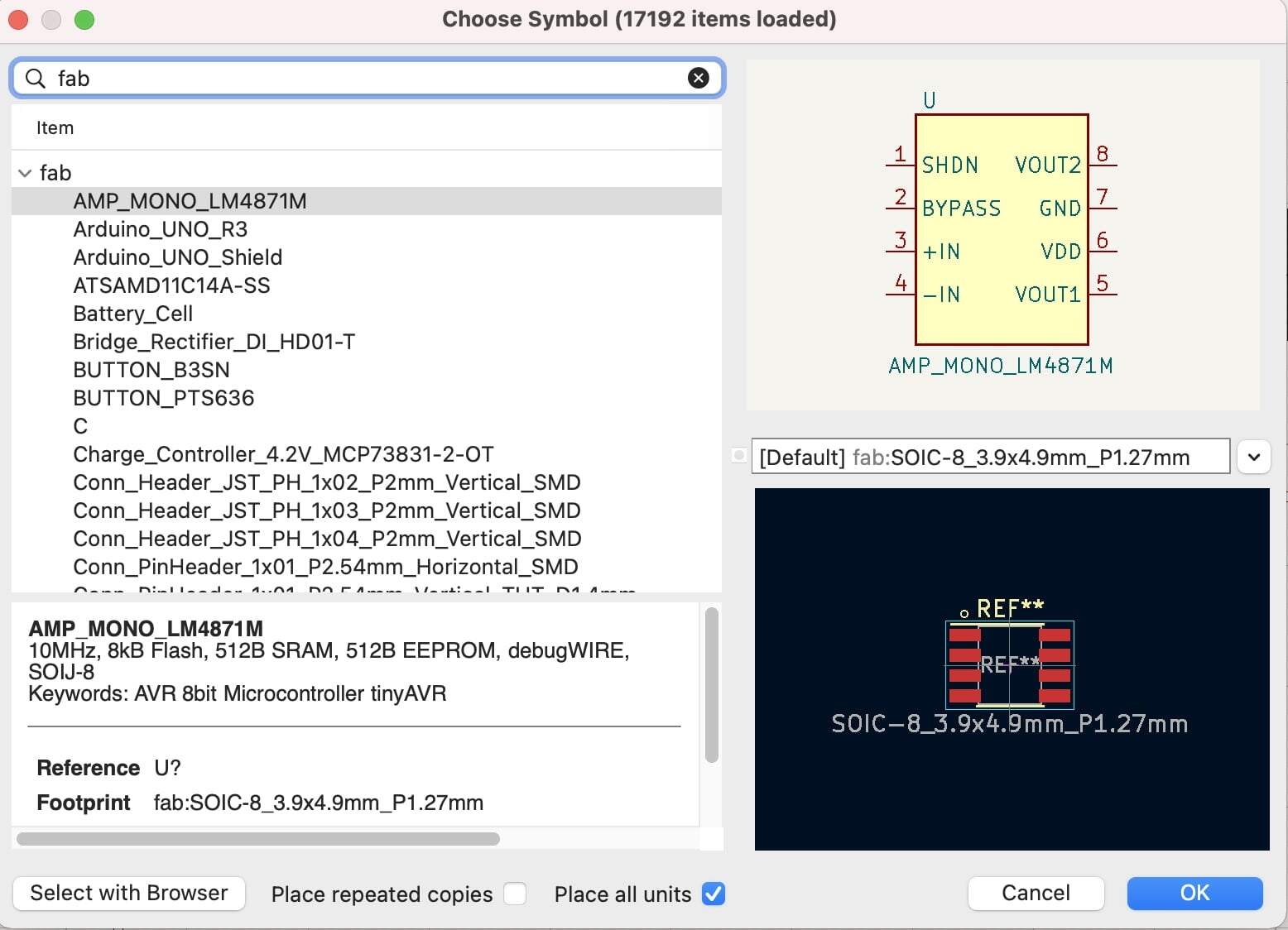
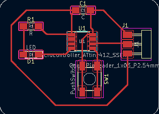
Now that I had the fab library, I could finally add in the symbols and footprints of the components I wanted. I went to the right sidebar, clicked the add symbol icon, which brought up the list of all the components. For each component, I searched up its name in the library, brought it out onto the canvas. Then I activated each’s footprint by going to the footprint library, searching the correct footprint, and then hitting the checkbox next to show footprint. These ended up being the symbols I used in KiCAD. - Microcontroller_ATtiny412_SSFR (Fab ATTiny412) - R (Generic Resistor) - LED (Generic LED) - SW_Push (Generic Pushbutton Switch) - Conn_PinHeader_1x03_P2.54mm_Horizontal_SMD (Surface Mount 1x3 Horizontal Header) I made sure to annotate each of the symbols. Thne these were the corresponding footprints I used - fab:SOIC-8_3.9x4.9mm_P1.27mm (ATTiny412) - fab:R_1206 (Resistor) - fab:LED_1206 (LED) - fab:Button_Omron_B3SN_6x6mm (Pushbutton) - fab:PinHeader_1x03_P2.54mm_Horizontal_SMD (Headers)
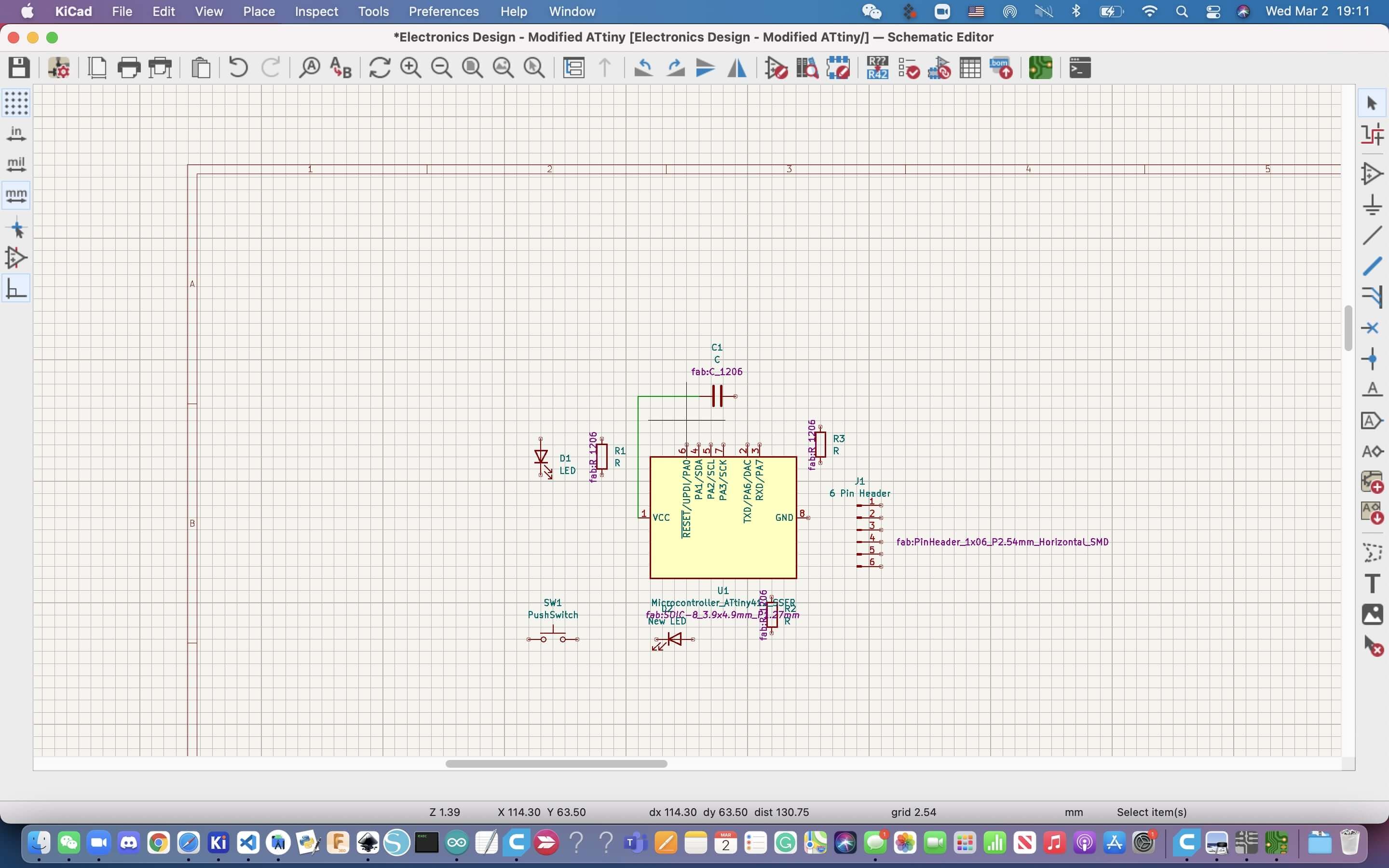
This is what the schematic looked like at this point
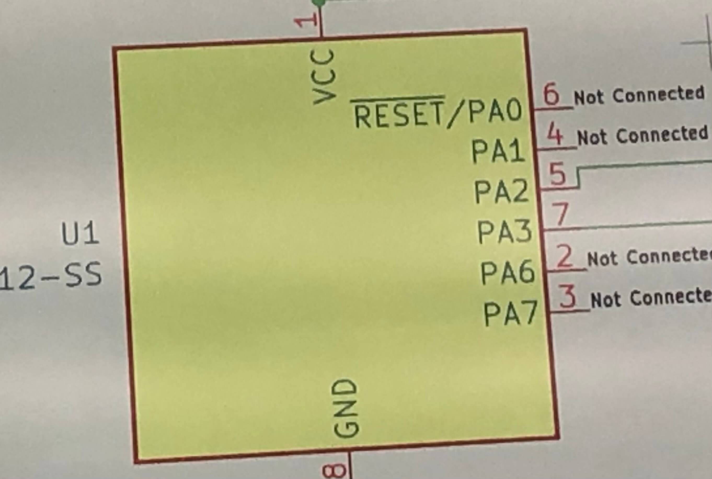
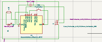
Now the final steps for the schematic were to add in the wiring and perform an Electrical Rules Check. I first focused on the ATTiny412 and I noticed that it had 8 pins. However I thought I only needed 4 of them - 1 power, 1 ground, a data line for the button, and a data line for the LED/Resistor. At first, I wired the schematic up like this, using the PA6 and PA7 pins of the chip.

After performing an Electrical Rules Check however, I discovered at least 3 mistakes I had made. Firstly, I had completely forgotten about the UPDI pin, which was pin RESET/UPDI/PA0 on the ATTiny412. To fix my mistake I simply wired this pin into the middle pin 2 of the headers, since I had already designated the top pin as ground and the bottom pin as power. I also changed the wiring from PA6 and PA7 to PA1 and PA2.
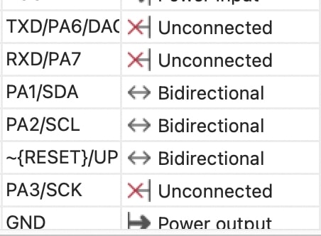
Secondly, the ERC told me that I had left pins unused on the ATTiny412. Normally, its completely fine to have unused pins on a microchip, but in KiCAD, it assumes that every pin will be used in some way unless you tell it to disconnect. At first I had no idea how to disconnect pins exactly and I was just going to ignore the message, but then Mr Dubick explained that it is still generally best to disconnect the pins in the schematic so the ERC won’t give error messages later on. He then explained the process of disconnecting pins in KiCAD.
I simply right clicked the ATTIny412, and went to the Edit with Symbol Editor option. Then in the symbol editor, I right clicked on one of the pins, and brought up the pin table. Next I went through the table and edited the status of the pins to unconnected. Going back to the schematic, I saw the changes, as now the pins that weren’t being used had an X over them. This is the pin table.
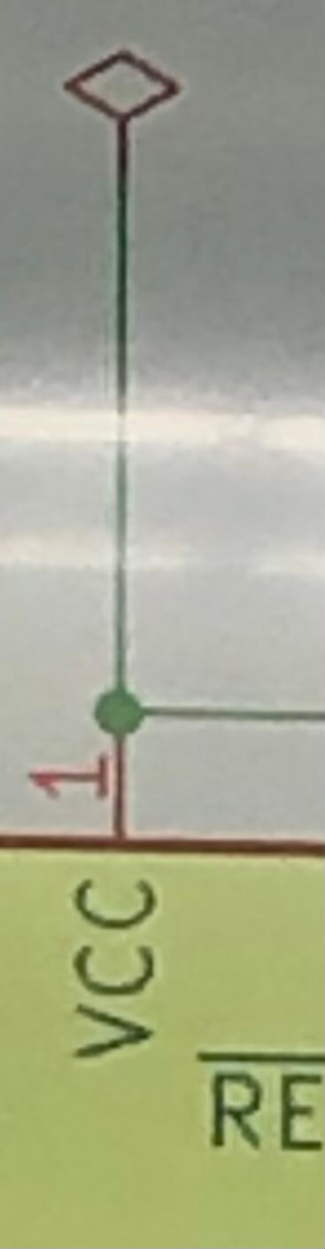
The third issue I had was the absence of a power flag. Just like unused pins on a microchip, KiCAD doesn’t like it when your schematic doesn’t include a power source. Obviously a circuit needs power to function, and I was going to be supplying power to this chip through a SAMD board, but KiCAD doesn’t know that, and thus it’s concerned that there’s no batteries or anything to give the circuit power. A power flag basically tells KiCAD that you will be supplying power externally, and thus adding it will help you pass the ERC. This is what a power flag looks like, and I just put it on the VCC pin of the ATTiny412.
After I fixed these issues, I ran the ERC again with no issues. This was my finished schematic.
Next, it was time to design the PCB in PCB Editor. I opened up the Electronics Design - Modified ATTiny412.pcb file, went to the top, and then clicked on the “Update PCB with changes made to Schematic” icon. Then I went to the edge cuts layer, and drew a rectangle to signify the edges of the PCB. This is what it looked like at this point.
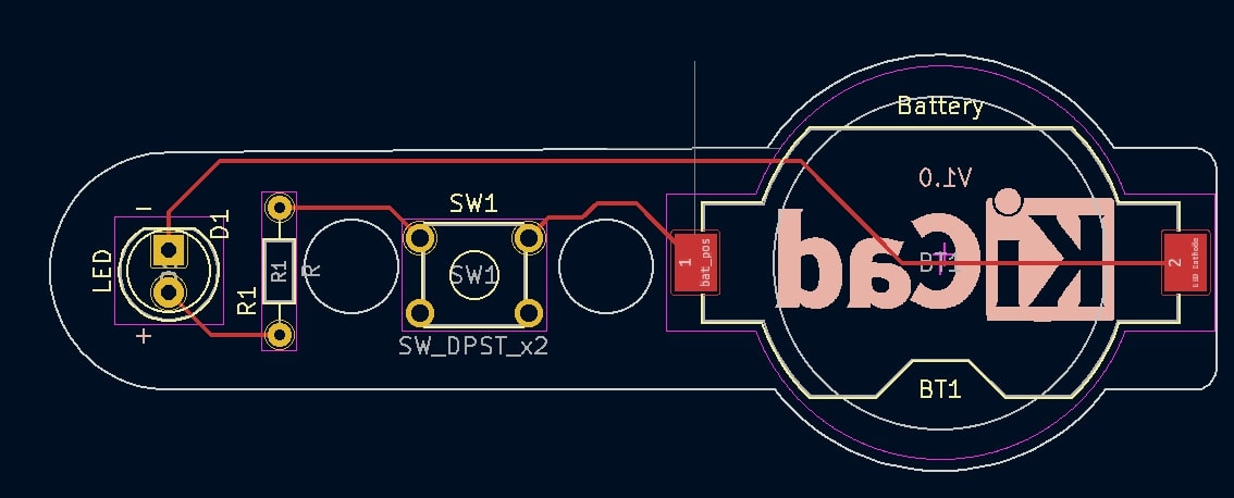
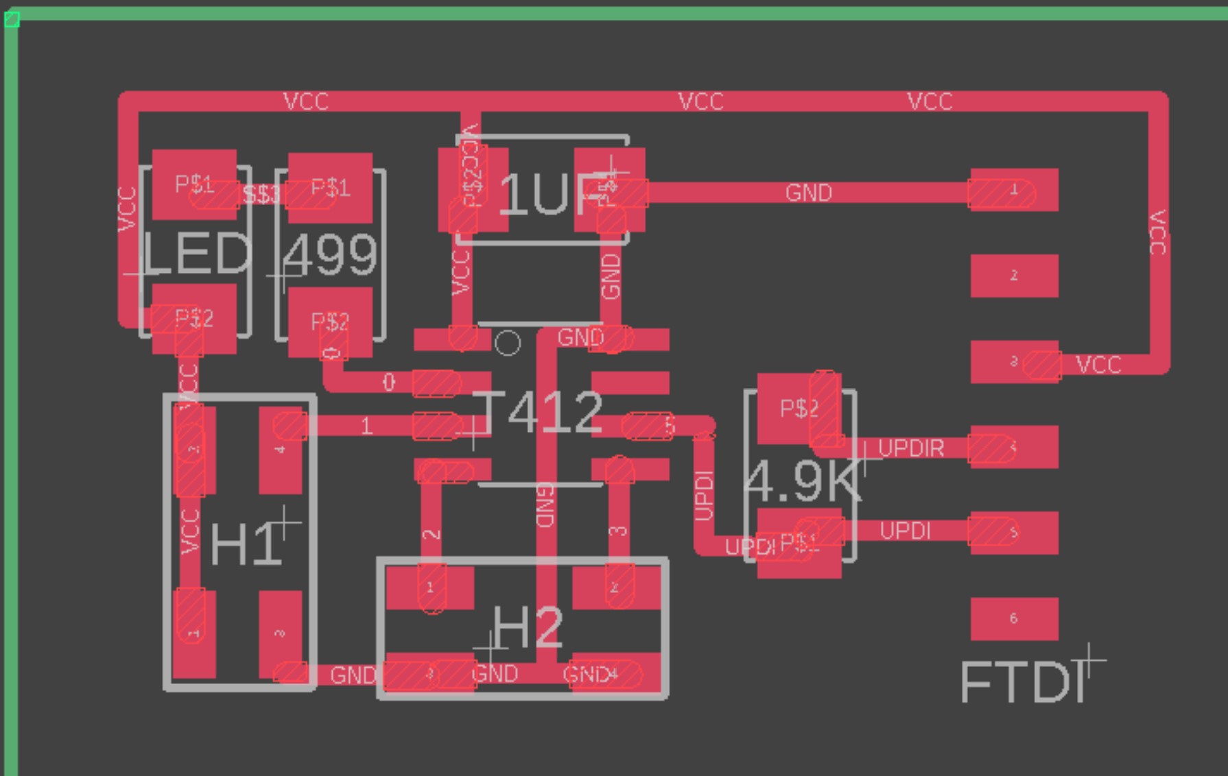
Now it was time to organize the components and track them together. Since I had already created all the wires in the schematic, I could basically go off of those lines and create the tracks. For organizing where the components would go, I had a bit of trouble deciding how each component would be best oriented. I ended up referring to this design by Mr Dubick to get a good idea of how to place everything except the pushbutton, and then added the button to the design.
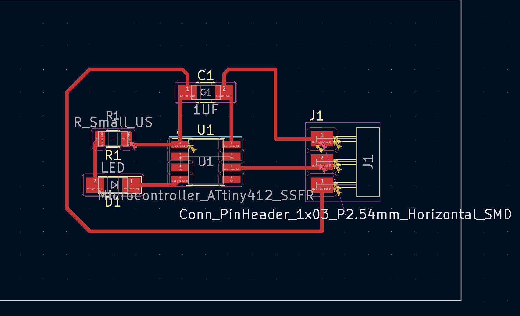
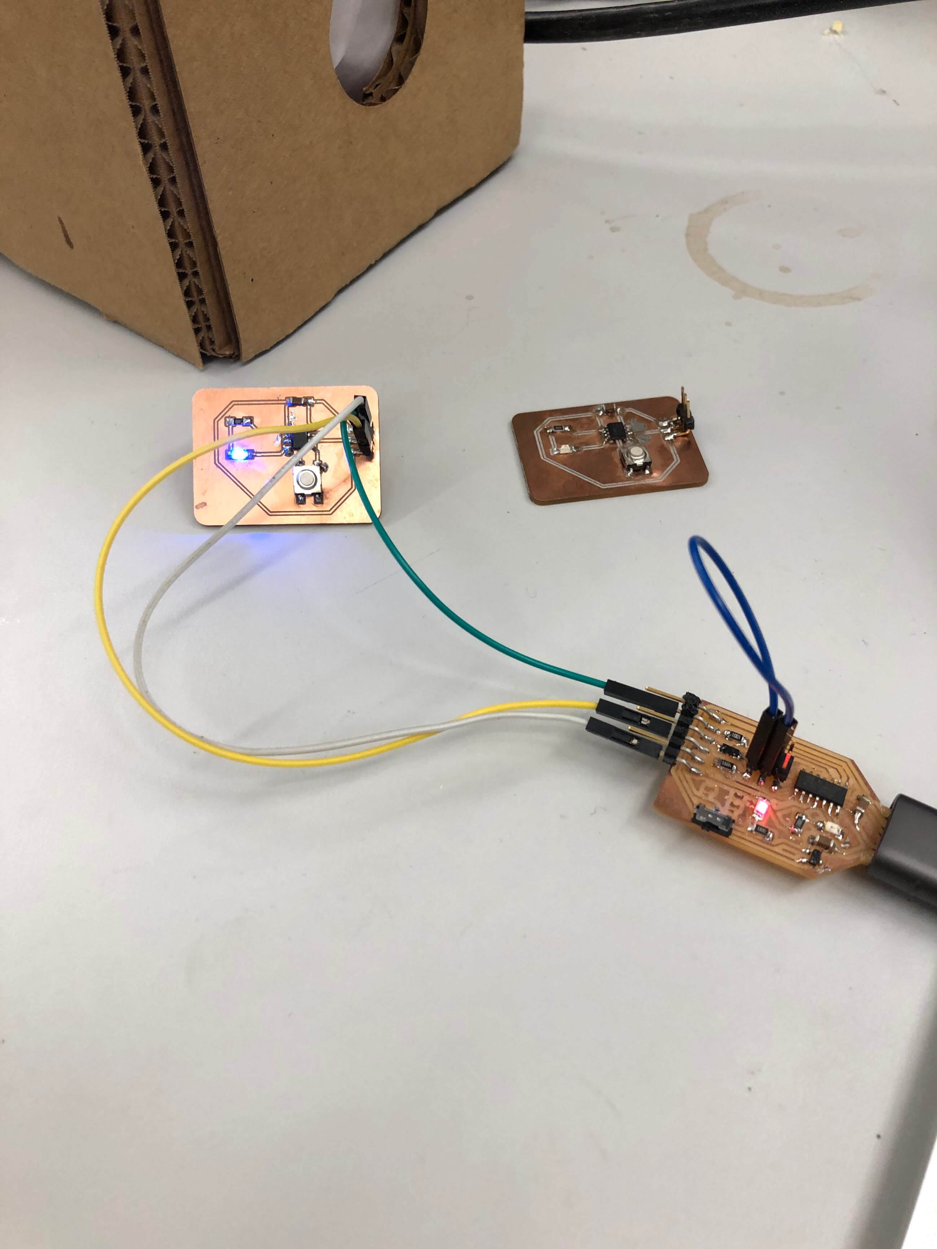
Here is the my finished design for my PCB, and as you can see, it is very similar to Mr Dubick’s design. One thing that is different is the edge cuts are curved instead of being a rigid rectangle. Another unique aspect about my board would of course be the pushbutton, which is wired from pin 5 of the ATTiny412, under the chip, into the power slot.
The final step in the process was to export the gerber files from my design. I did this in the PCB Editor by going to File -> Fabrication Outputs -> Gerber, which pulled up this popup.
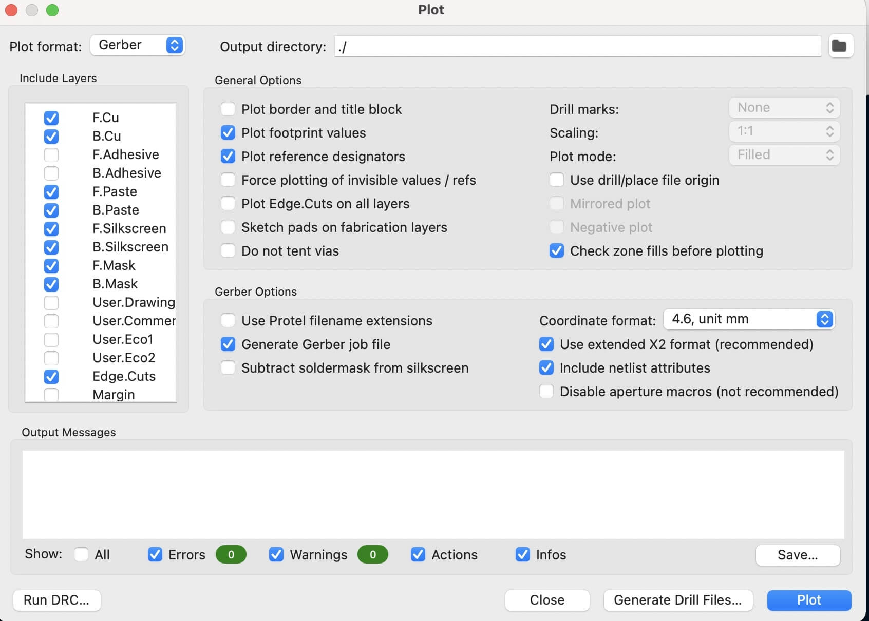
Then I hit plot, and generate drill files, and took those files to the milling machine. Overall this week was pretty educational since I got exposed to Electronics Design for the first time.
Milling and Soldering
For milling out the PCB, I pretty much followed the exact same workflow as the last time, with a few minor changes. Here is the link to the updated workflow for our lab’s milling machines.
Note: Because I have already documented PCB milling extensively in Week 05: Electronics Production, I will only be including the steps I took to mill one of the boards. I did have to repeat this process twice though as my first board wouldn’t even receive power.
First I brought in my gerber files into the Bantam software by going to File -> Open, and opening up the files. In the prompt that resulted, I made sure to have the F.Cu (Front Copper) file loaded on the top layer, and the Edge Cuts layer loaded on the outlines. Then I cleared the Bottom and Holes layers of the design, and hit ok. Next I had to select the tools I would be using for milling, which were the 1/64 end mill for the traces, and the 1/32 end mill for the outline. This is different from previously when I used the PCB 0.005 bit for the traces, and this change is because the 1/64 bit cuts cleaner traces than the PCB one. Then it was time to load the 1/64th bit into the software. After clicking Change Tool -> 1/64 end mill -> continue, it prompted me to locate the tool.
After locating the tool, I went under BitBreakers -> Probe Material Thickness, moved the spindle over the part where I was milling, and this resulted.
I then hit mill all visible and it began to mill out all of the traces for my PCB. After the traces were milled out it asked me to locate the tool for the 1/32 bit.
Then it began to mill out the edge cuts using the newly added 1/32 bit.
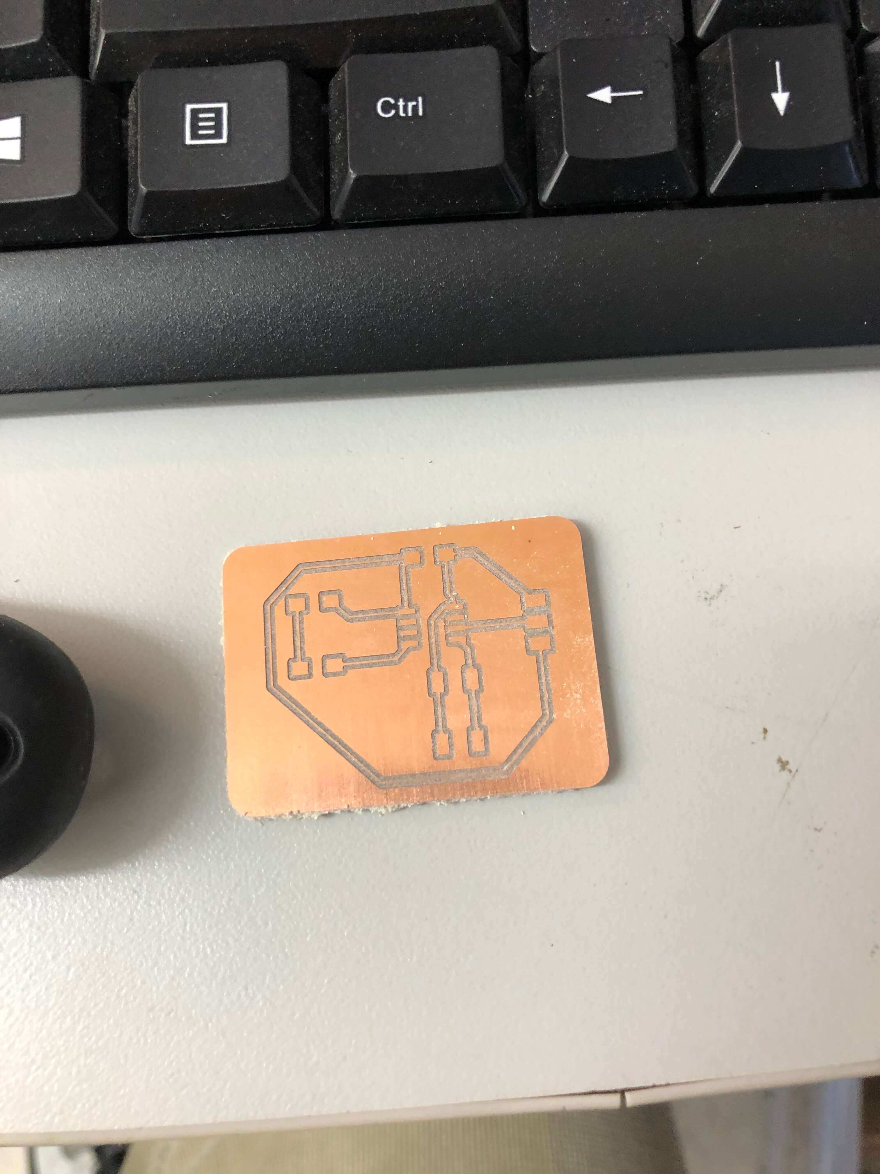
This is what the milled board looked like. Overall, the traces were very nicely milled but the only thing I would change for the next time would be the trace width and trace clearance as these made solder bridges very common when soldering.
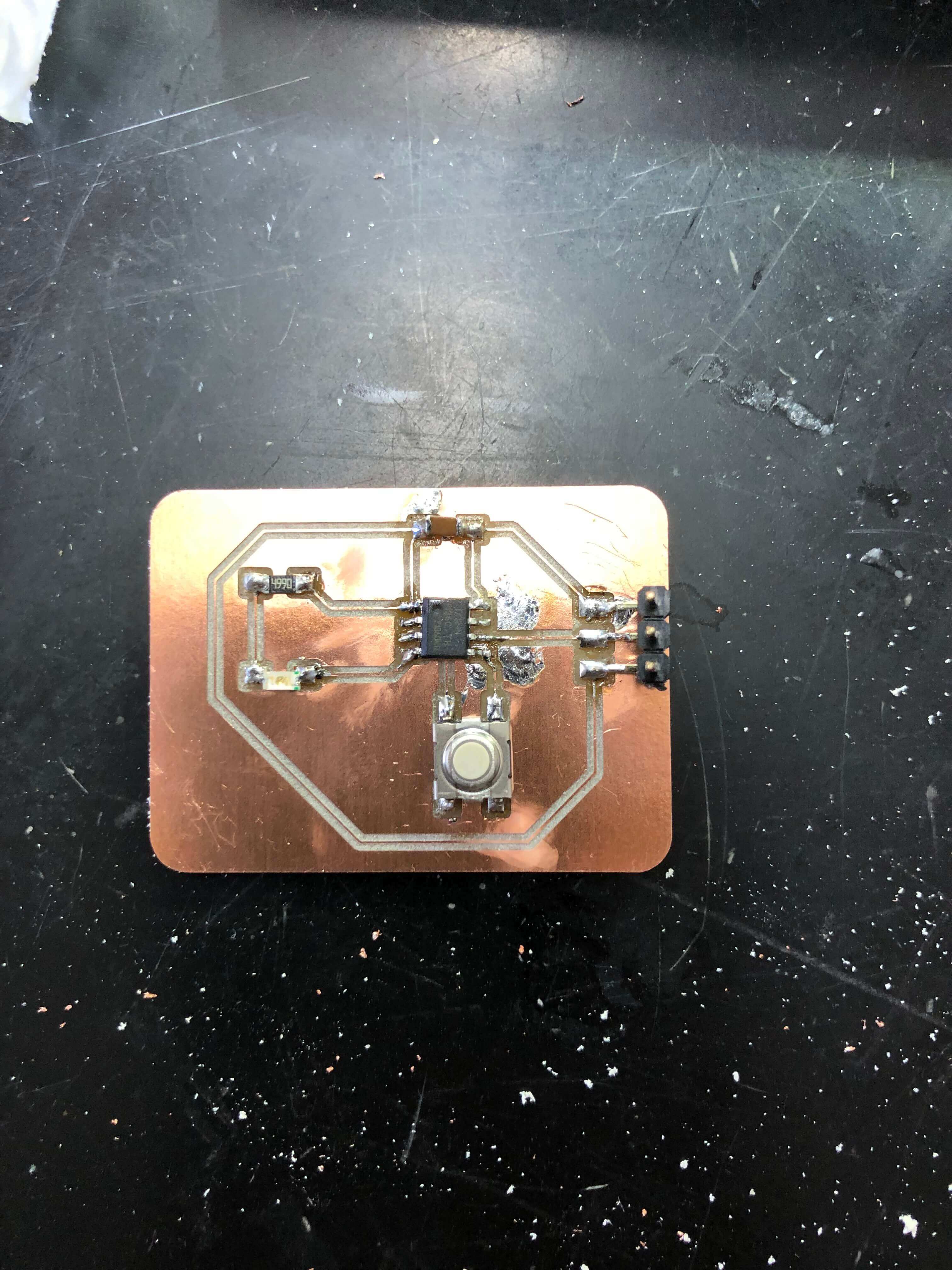
For soldering the board, I used the method of soldering one pad, securing the component with tweezers then soldering the other pad. Unlike week 05, I did not have as many issues with soldering because this board was simpler and I am better with soldering now. I referred to my PCB layout in KiCAD, and it was very easy to figure out which component went where.
Programming
Once I had the board milled and soldered, the final step was to make sure it worked by flashing a simple program to it through the SAMD11C programmer we made previously. The first time I supplied power to the board, the LED did not immediately turn on, but after fixing a soldering mistake, the LED finally turned on.
For the actual code, I just took the TinkerCAD example code and modified the pin numbers to fit my board since I was not using an Arduino but an ATTiny412. I referred to this ATTiny412 pinout sheet to figure out which pins to flash the button code to. At first I kept getting this error when flashing the code to pins 4 and 5.
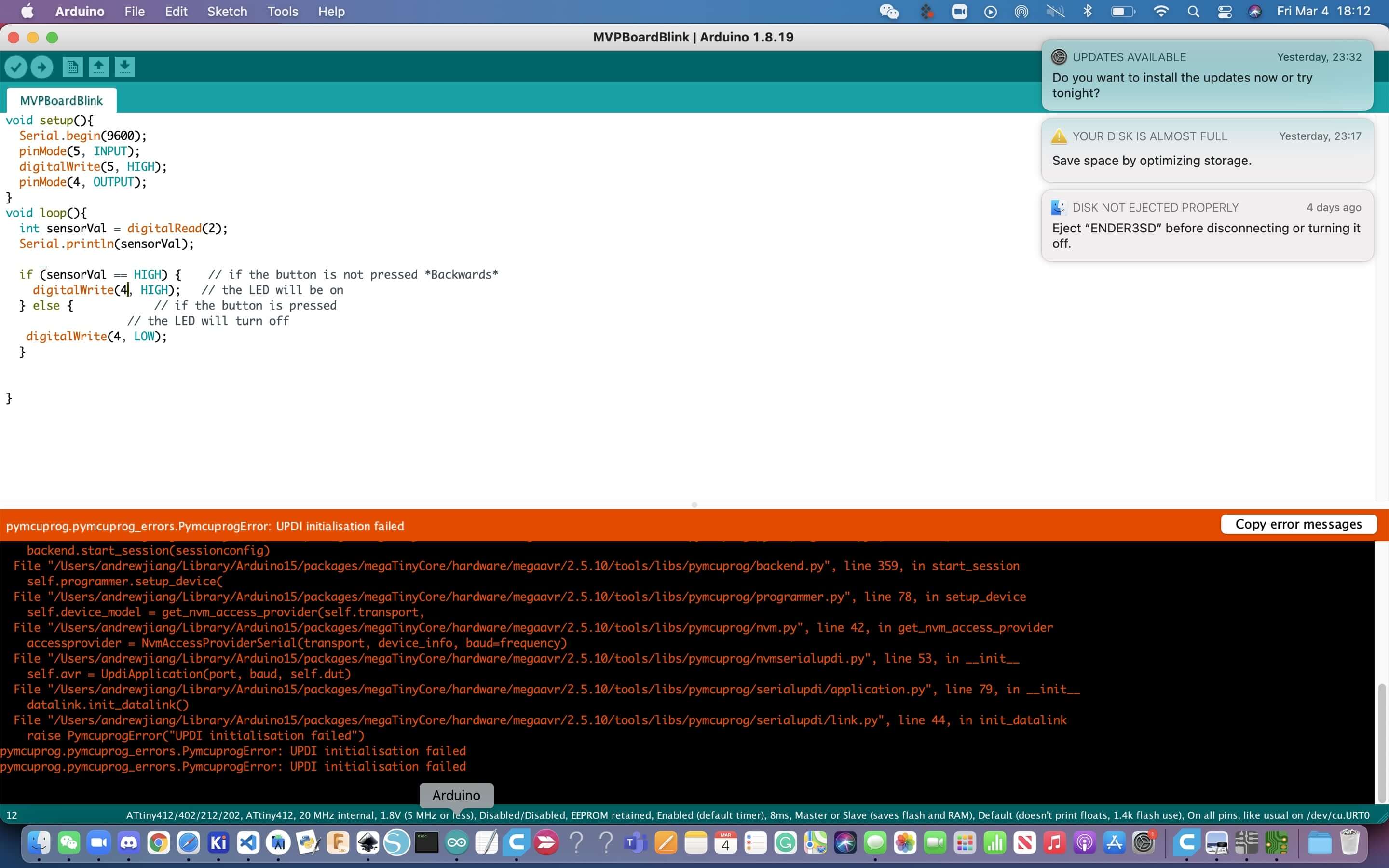
Then I realized my mistake, which was that I was using the wrong pins. Instead of using pins 4 and 5, I should have been using pins 2 and 3 instead. When I switched the code, this is what the code looked like.
void setup(){
  Serial.begin(9600);
  pinMode(3, INPUT);
  digitalWrite(3, HIGH);
  pinMode(2, OUTPUT);
}
void loop(){
  int sensorVal = digitalRead(2);
  Serial.println(sensorVal);

  if (sensorVal == HIGH) {    // if the button is not pressed *Backwards*
    digitalWrite(2, HIGH);   // the LED will be on
  } else {            // if the button is pressed
                  // the LED will turn off
   digitalWrite(2, LOW);
  }


}
This is the output from the working UPDI code

This is the final test that proves that my board works. As you can see it employs a pull down resistor that doesn’t light up the LED until the button is pressed.
Week 07 Group Work
This week’s group assignment was to use the test equipment in your lab to observe the operation of a microcontroller circuit board. Our lab has two main types of test equipment: oscilloscopes and multimeters. Aarush, Pari and I were tasked with testing the multimeters.
The digital multimeter is a tool that can be used to measure a variety of functions, most commonly used to measure Voltage, Current, and Resistance. In this case, Andrew and Aarush used it to measure the operation of Pari’s hello world PCB.
Diode Checker
A multimeter’s diode checker produces a small voltage between the two test leads that allows us to see the actual forward voltage of the diode when its conducting current. We used the multimeter to check the operation of the LED on Pari’s board. As you can see, the LED emits light when the multimeter probes are held to it. This shows that the LED is functional and isn’t burnt out.
Voltage
Then we all tested the voltage. Voltage is expressed in Volts, so we tried to see how many volts the board has. For an LED to turn on and have power, it needs 5.00v To check we had the proper power and the board did not lack power, we measured the voltage on the power trace, and the multimeter read around 5v.
You can find more information about this week’s group work here
Week 07 Files
Click here to access my files for this week