7. Electronics design
This week our assingment was to redraw an echo hello-world board.
These were my files for this week.
I first went to see what an echo hello- world board was. My instructor Mr. Dubick provided one his board as a referecnce and so did Mr. Harris
Here are the two boards that I used as a referecne to draw my schamtics.
Dr. Harris’s Board
Mr. Dubick’s Board
Design process
To start the design process, I used KiCad, although before designing the Echo hello-world board, I followed some toutrials from Tech Explorations on how to navigate KiCad and followed along on how to build a basic PCB Board. The toutrials taught me how to choose and place components, connect wires, make a PCB, and export the files to mill.
After following these torutrials I downloaded a fab acasdmey library for all the components which will be needed to make the echo hello-world board. Here is the library which I downloaded.
After downloading this library I went adjusted the setting by going into:
- Preferences > Symbol Library > Select fab.kicad_sym. This uploaded the symbols into the preferences, which will be used later on to make the schmatic.
Next I went into: - Preferences > Manage Footprint Library > Select the directory with all the downloaded files.
Finally, I went into: - Preferences > Configure path > Select directory where the files are downloaded
After completeing all these steps, I added the following components which was be used on my baord.
The comonenst that I used are:
- ATTiny412 chip
- Capacitor (not polarized)
- 499k Resistor
- LED (Red)
- Male Connector Headers
- 4 Pin Button (although I recommded a 2 pin button)
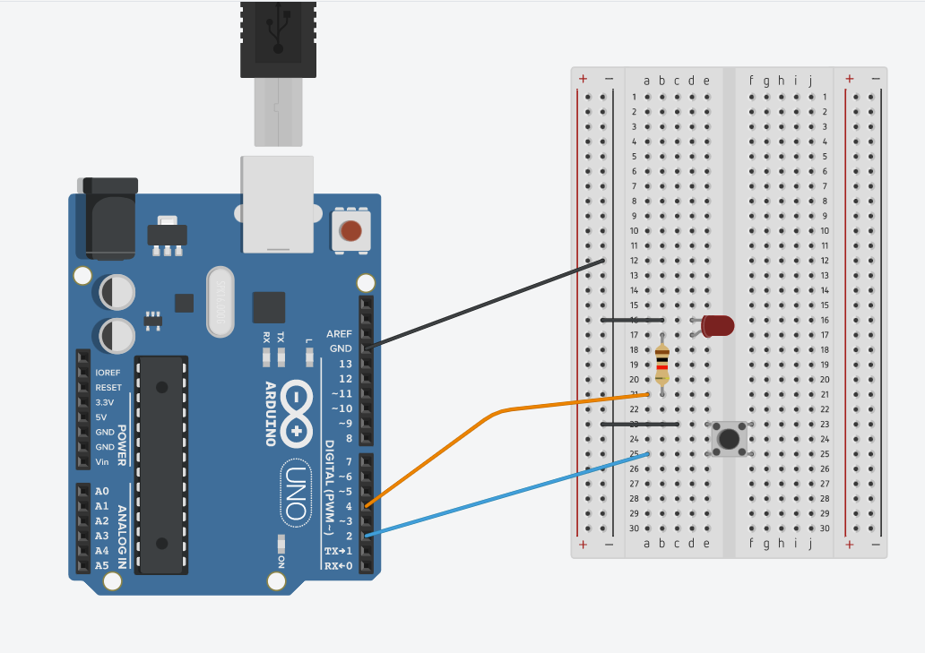
I first made a schmatic on TinkerCad and wrote code to make sure I understood the basic concept of what the assignment was. In short words my goal was to make a pull-up resistor. This meant that when the button is pressed the LED would turn on, and when not pressed the LED would tun off. This sounds pretty straight forward and simple, but in reality it was a little challgingto rap my mind around it.
Here is the schmatic from TinkerCad, I used and ardunio instead of a Attiny 412 chip.
TinkerCad Schematic
This is the code I wrote for it:
void setup() {

  //start serial connection

  Serial.begin(9600);

  //configure pin 2 as an input and enable the internal pull-up resistor

  pinMode(2, INPUT_PULLUP);

  pinMode(4, OUTPUT);

}

void loop() {

  //read the pushbutton value into a variable

  int sensorVal = digitalRead(2);

  //print out the value of the pushbutton

  Serial.println(sensorVal);

  // Keep in mind the pull-up means the pushbutton's logic is inverted. It goes

  // HIGH when it's open, and LOW when it's pressed. Turn on pin 13 when the

  // button's pressed, and off when it's not:

  if (sensorVal == HIGH) {

    digitalWrite(4, LOW);

  } else {

    digitalWrite(4, HIGH);

  }
}
After making my TinkerCad circuit work, I followed that same schemtic into KiCad.
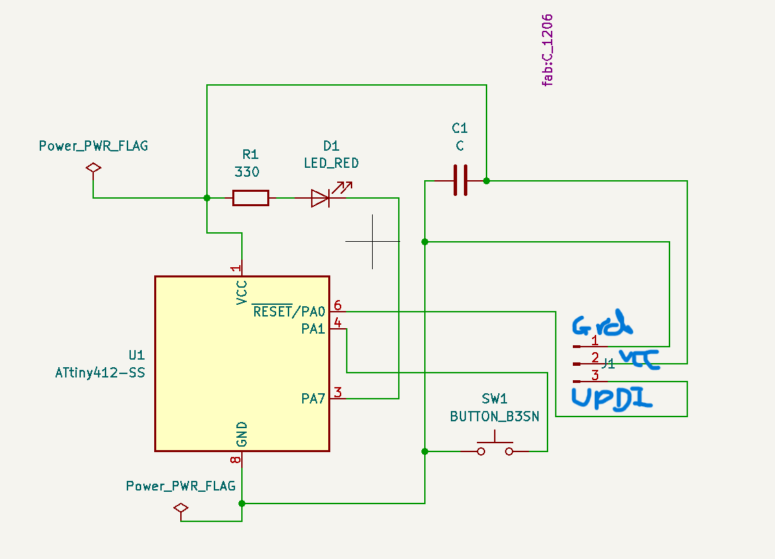
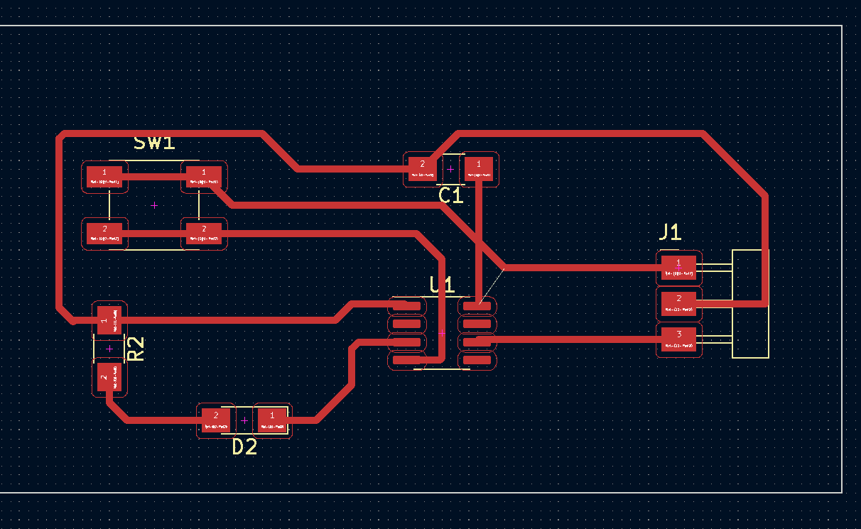
I first connected my header pins to the Attiny 412 chip and assigned them the values of ground, power (VCC), and UDPI. After doing all of this and making sure verything is right, I turned the schemtic into a PCB Editor. This is where I would actually design the board and draw the traces.
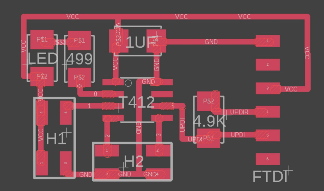
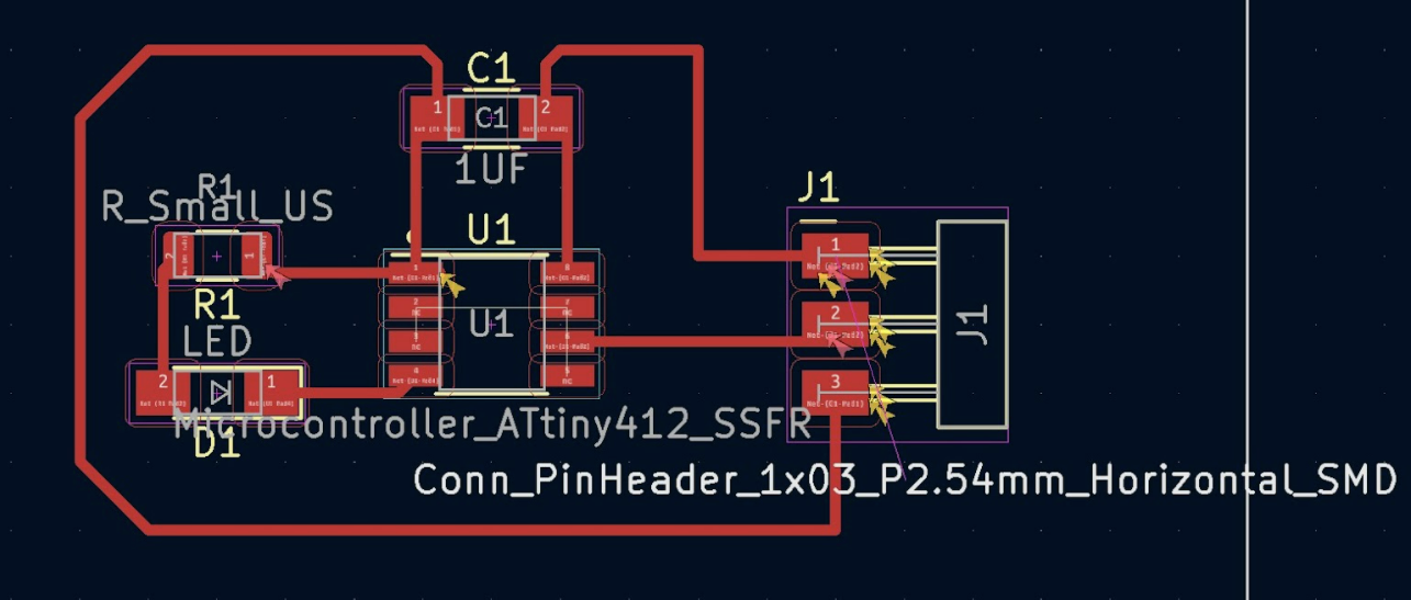
Schamtic
In the PCB Editor I arranges the componets so that the were organized and the traces wouldnt overlap each other. This is an art and takes a while to get right, I struggled a little, although followed the reference boards of Mr. Dubick and Dr. Harris.
PCB Editor
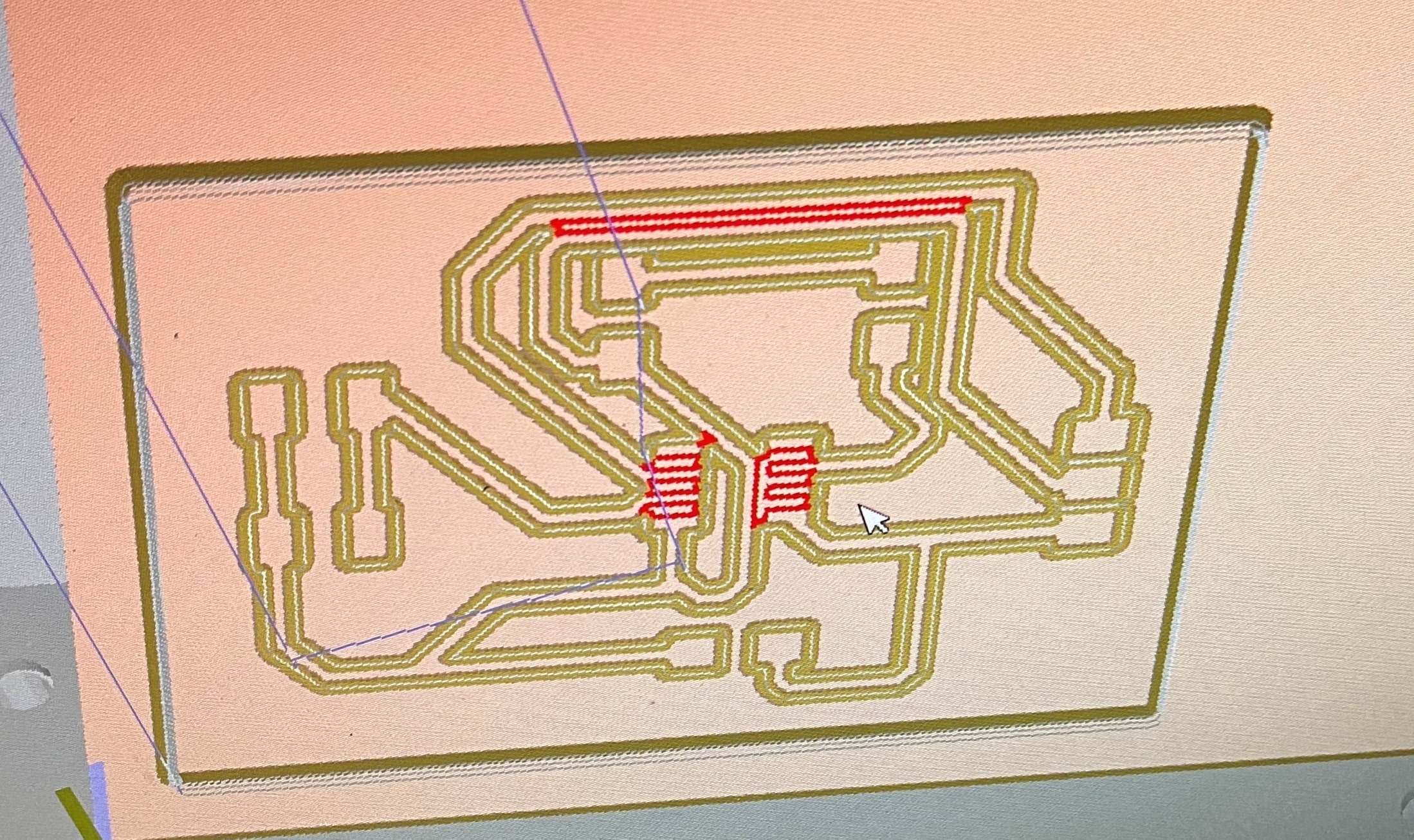
After designing the board, it was time to export it. To export these boards you follwo these simple steps:
1 . Go to file –> plot
WHile in this feature, select all the layers that you want to have on your board when it is milled. For this board, I chose the Edge Cuts layer and the Front Copper layer.
These were the layers I drew my components and had my designs on.
2 . After selecting the desired layers, click “Run DRC” and then after click “Plot”.
3 . Now the files are svaed to my directory and I can export them to Google Drive.
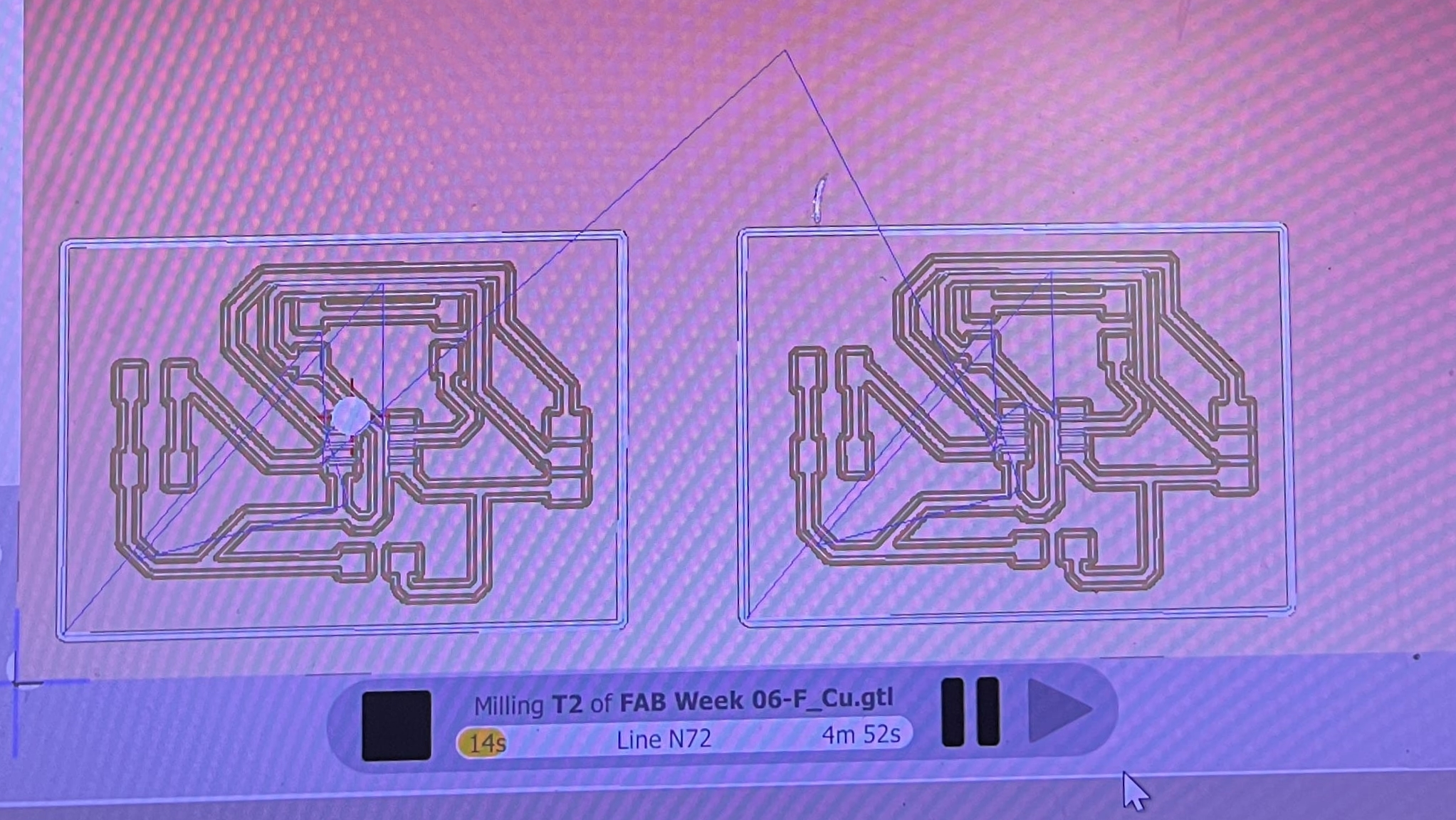
Milling
To start bthe milling process I followed the same workflow as I did during Week 05.
Milling on Bantam Tools Workflow
I followed the workflow and started milling my board.
Board Fail #1
The fist board I milled was a little rough. The traces were a little thin and there wasa lot of left over copper residue. Coppper residue may shoet boards if the wrong reside touches other traces. I did not realize this at first, so I decided to soder the components on the board and tried to program the board. As was expected the board did not work. I went back and tired to clear the traces with an exacto knife, and then went back and tried to reprogram my board. It did not work, so I then decided to mill a new board.
Settings Of The Bits I Used:
| Test Try | Bit 1 | Result | Solution |
|---|---|---|---|
| Fail #1 | 1/32 in Flat End Mill | Narrow traces | Changed bit |
Board fail #2
On this board I did everything the same, except used a 1/64 in Flat End Mill. The board milled put succesfully and I sodered the componetnts on. The traces looked 10x much better and there was no loose copper residue. After sodering all the components on, I tried to test my board and see if it worked. Still no result. This became frustrating and I thought my code was wrong, although I leanred after thst it was not. On the next board, I finally read the workflow CAREFULLY and saw that there were different trace depth’s and clearnces which had to be used. I finally then milled out a 3rd board.
| Test Try | Bit 1 | Result | Solution |
|---|---|---|---|
| Fail #2 | 1/64 in Flat End Mill | Narrow traces | Changed trace clearnace and depth |
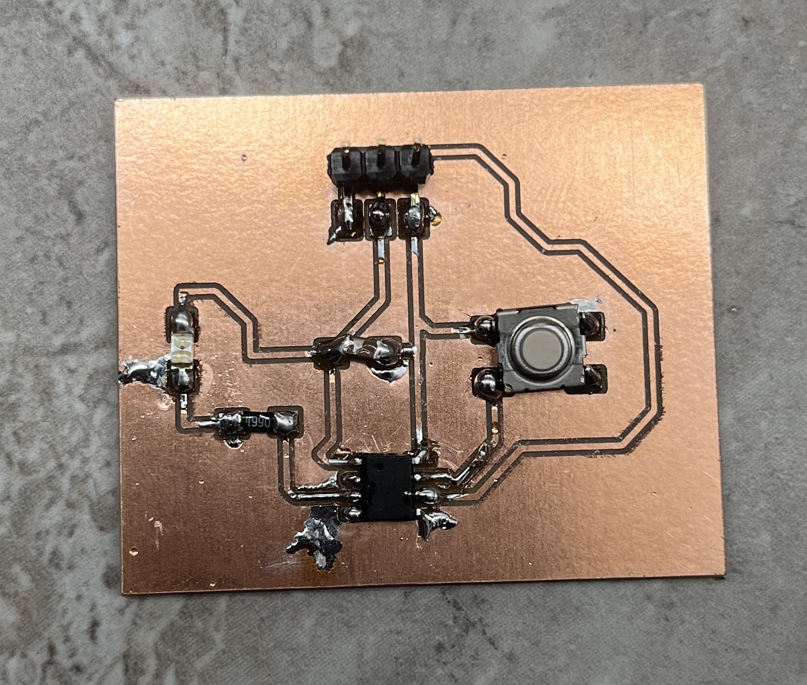
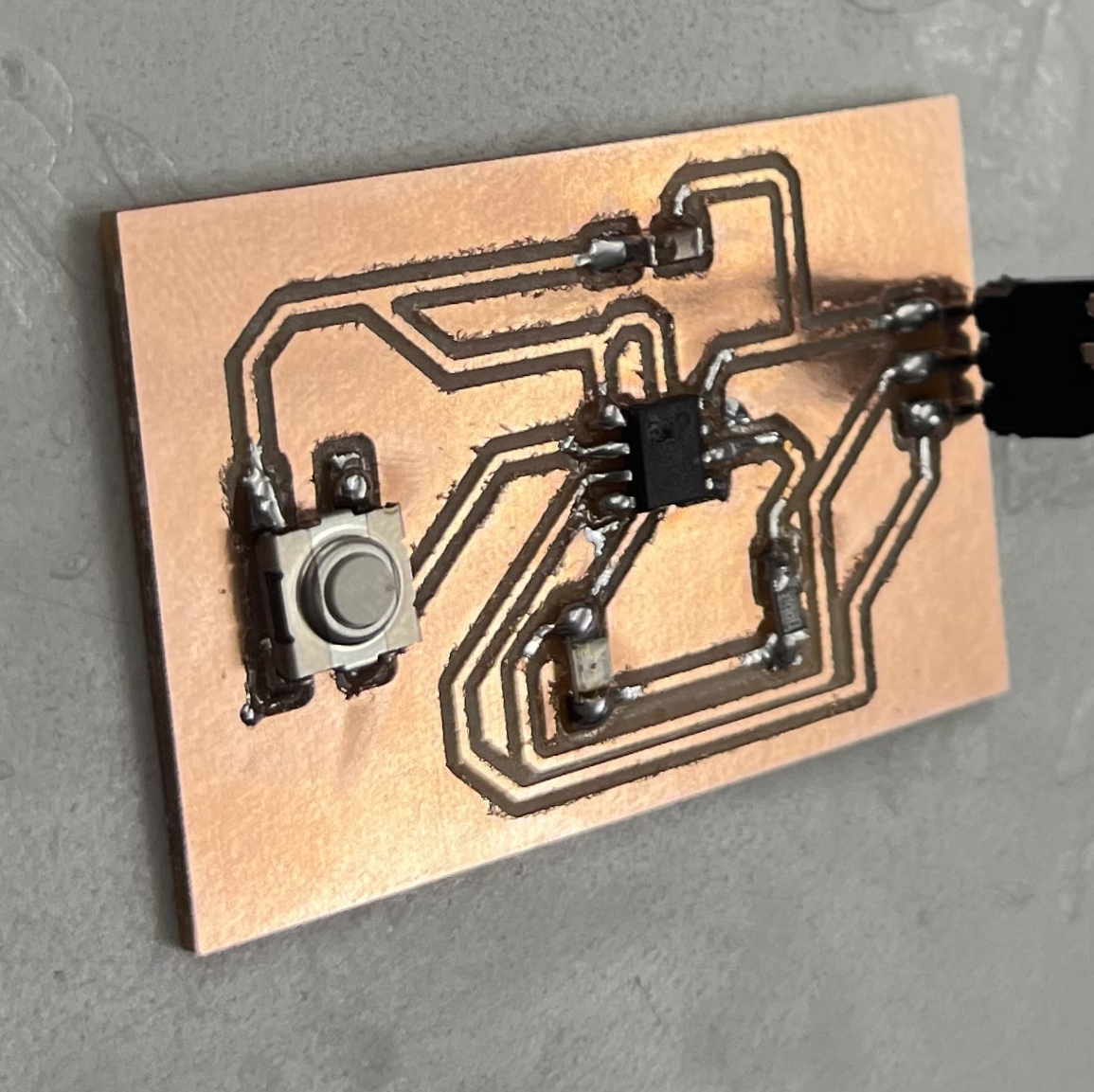
Board Success #3
FInally after reading EVERYTHING on the workflow, I fianlly changed the trace clearance to 1.50 mm and the trace depth to 0.20 mm. I set up everythign as pe the workflow and did not work of memorization. I milled out the final board, and it fianlly looked nice and functional. After the many soder sttempts previously this board took my less than 5 minutes to soder. I sodered all the components out, and then tested it out with an Arduino. I used Mr. Dubick’s computer because, I wanted to elimate any mistakes that could happen. After HOURS and HOURS of work, this finally paid off. My board started to blink and thr LED turned on.
| Test Try | Bit 1 | Result | Solution |
|---|---|---|---|
| Fail #3 | 1/64 in Flat End Mill | Perfect Board | Fab Student does happy dance :) |
Challenges in Milling and PCB Design
Some challgenes I ran into were very little. In the future, I should make sure to keep the UPDI in the middle so I do not mix up ground and power(VCC). Another challnge I ran into was trace clearnace and depth, although that could have been aviod if I had thorughouly read the workflow.
Take aways from Milling and Designing
I feel MUCH more comferatbel milling and designing a board now, and I think I can do it myself now by having a refernce board to refer to. I am starting to grwo a liking for electromics even though I stryggle with it at times. Maybe this can be my segway into going to Electrical engineering in the future! I love a good chalggned and I love dolving challegnes, and I really enjoyed this week (thinking about it as I am documenting)
Software
After sodering on all the components it is time to upload software to my board.
This was a tedious process, although at the end I finally inderstood the logic behind the code of a pull up and push down resistor.
Uploading the softeare was a failty simple process.
1 . First, you should open Arduino, connect the Arduino to a port of your computer.
2 . Upload the code above or this code blow and change the pin outs by follwoing the pin outs of an ATiny 412 chip
Here is what the board wiring looks like:
void setup() {

  //start serial connection

  Serial.begin(9600);

  //configure pin 2 as an input and enable the internal pull-up resistor

  pinMode(2, INPUT_PULLUP);

  pinMode(4, OUTPUT);

}

void loop() {

  //read the pushbutton value into a variable

  int sensorVal = digitalRead(2);

  //print out the value of the pushbutton

  Serial.println(sensorVal);

  // Keep in mind the pull-up means the pushbutton's logic is inverted. It goes

  // HIGH when it's open, and LOW when it's pressed. Turn on pin 13 when the

  // button's pressed, and off when it's not:

  if (sensorVal == HIGH) {

    digitalWrite(4, LOW);

  } else {

    digitalWrite(4, HIGH);

  }
}
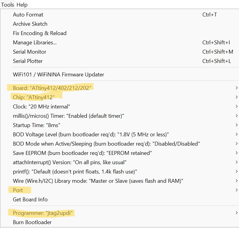
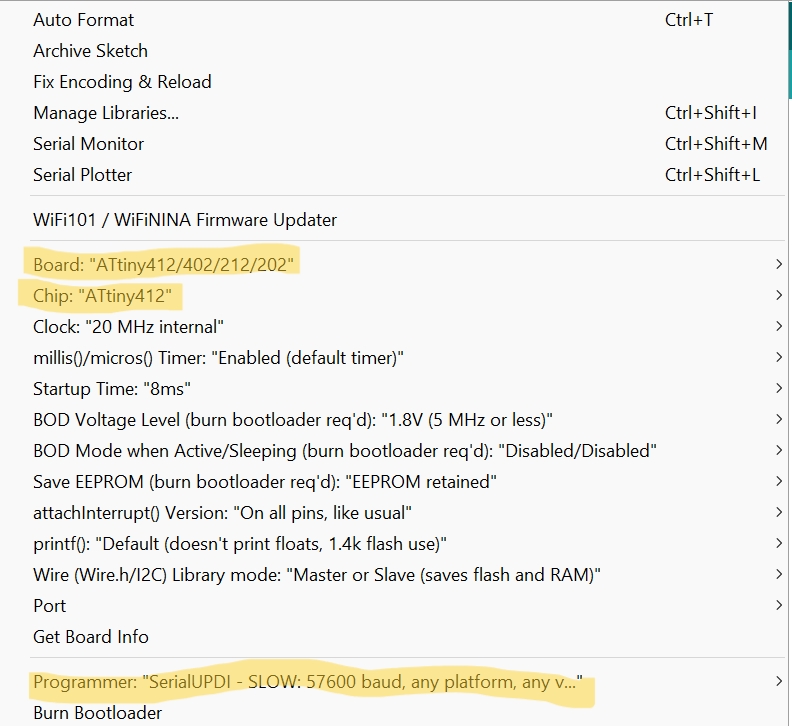
3 . After making adjustmets to your code, make sure to configure the tools section. By selecting the proper ports, programmers, and boards.
These were my settings:
4 . After carfully making sure your tools are correctly selected. It is time to upload the code and click verfiy and that should check the correctness of your code.
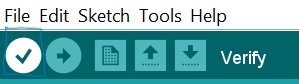
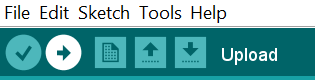
5 . Once the code is verfied press the upload button to upload the program onto the board!
6 . To know your board works, test it! See if the program yuou uploaded works!
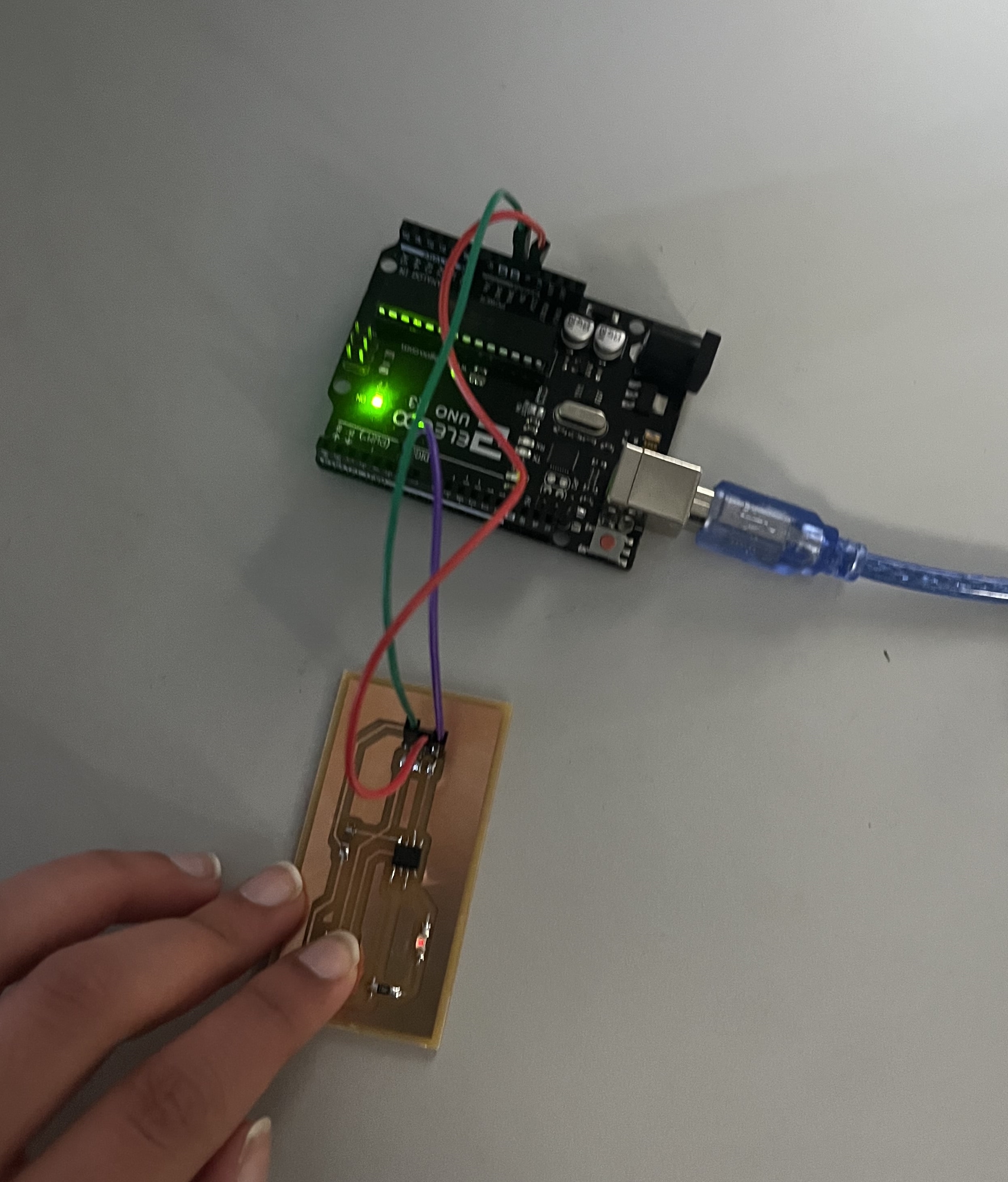
Here is my board working!
Board Working with Microcontroller
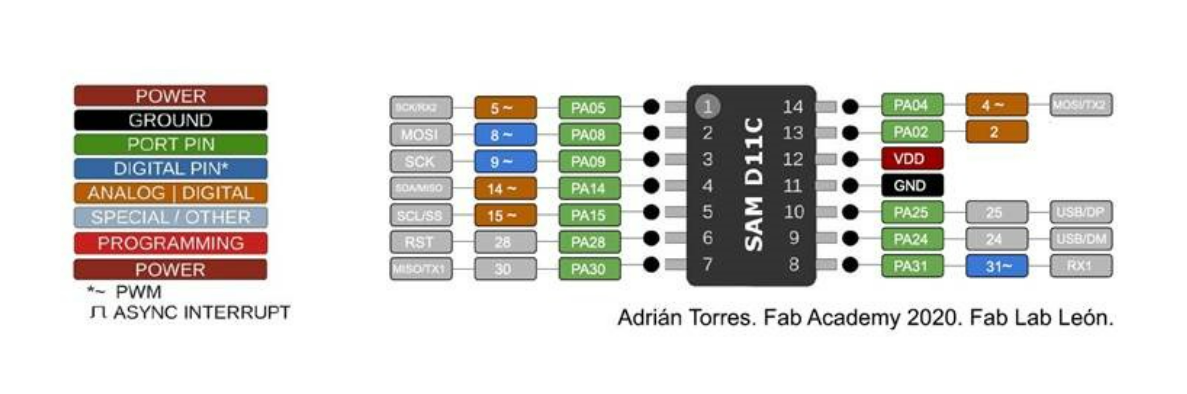
Using the SAMD11-C is super simple, although you HAVE to follow all your steps.
Here are the steps you should follow:
1 . Open Ardunio IDE, and copy/paste this code
void setup() {

  //start serial connection

  Serial.begin(9600);

  //configure pin 2 as an input and enable the internal pull-up resistor

  pinMode(2, INPUT_PULLUP);

  pinMode(4, OUTPUT);

}

void loop() {

  //read the pushbutton value into a variable

  int sensorVal = digitalRead(2);

  //print out the value of the pushbutton

  Serial.println(sensorVal);

  // Keep in mind the pull-up means the pushbutton's logic is inverted. It goes

  // HIGH when it's open, and LOW when it's pressed. Turn on pin 13 when the

  // button's pressed, and off when it's not:

  if (sensorVal == HIGH) {

    digitalWrite(4, LOW);

  } else {

    digitalWrite(4, HIGH);

  }
}
2 . Great! Now since you are using a 412, go to the tools menu and select you board and the type of programmer you will be using. These are the correct settings as shown below:
3 . Once you have done thse settings, put your Programmer into your computers USB Port, and upload the code!
4 . Voila! Your Board is programmed!
Learning from the Datasheet
Here is where you csn find the AtTiny 412 Data sheet. In this datasheet I learned about a built in resistor. So what it means is that when it is called upoj it acts like a pull up resisitor, hence I didnot have to add a button on my board.
Challeges
There were MANY challenges that I ran into, although all of them were fixed by increasing the trace depth and clearnce. If this had been done before most of my problems would have been fixed. One of the main challgneds i had was understand what extacly is a pull up reistor. Sicne this is all new to me it was for me to learn it quickly for this week. Although by the end of this week I learned most of it and feel like I could make this board again in less than 2 hours.
Take aways
I learned a LOT this week, and felt very satfilied after I achoved my main goal.
Things I learned:
1 . Never give up! ALways push and try your best, because you never know if the next method you try will work.
2 . Always read all the instructions on a workflow or anything. I missed somwething very important which could have saved a LOT of my time.
3 . Work slowly and accurantly, dont rush to catch up to others! Work no your own pace.
4 . Make sure to trust yourself! You are most likey right if you’ve leanred it before ans taken notes :)
Goal: Read all the instructions and don’t assume.
These were my files for this week.
Group Work
This weeks groups was to test the equipment in our lab to observe the operation of a microcontroller circuit board. In this week’s group work, I worked with Andrew, and Aarush to the current, voltage, and amps on my Blinky Board. This helped us take a deeper dive into what ground, power, and UPDI are.
This is our group site. Go check out our process for the group work this week!