14. Networking and communications
These were my files for this week.
This week’s assignment was to design, build, and connect wired or wireless node(s) with network or bus addresses.
Initial Idea
my initial idea was to make two LED boards communicate with each other. To do this, I would use RX/TX communication to talk/ network between both boards.
Designing the Boards
To start my designing I followed my Week 5 which shows me how to make a schematic.
I used KiCad to make my schematic, and this is what it ended up looking like. By now I have made tons of schematics so, I have become accustomed to all the available features.
I first started to design my Node Board. This board would receive signals from the Parent Board.
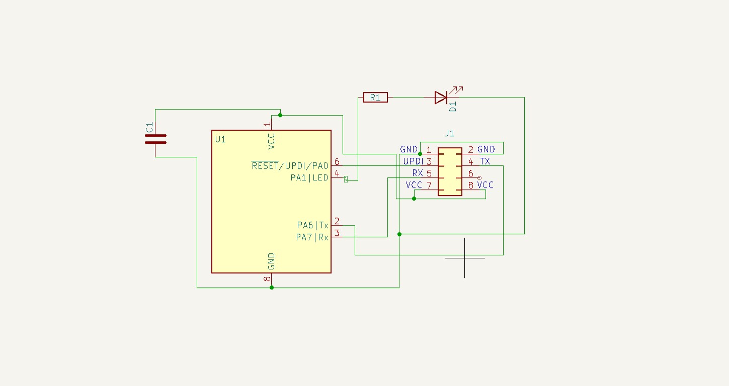
This is what my schematic looked like for the node board:
Schemtic for Node board
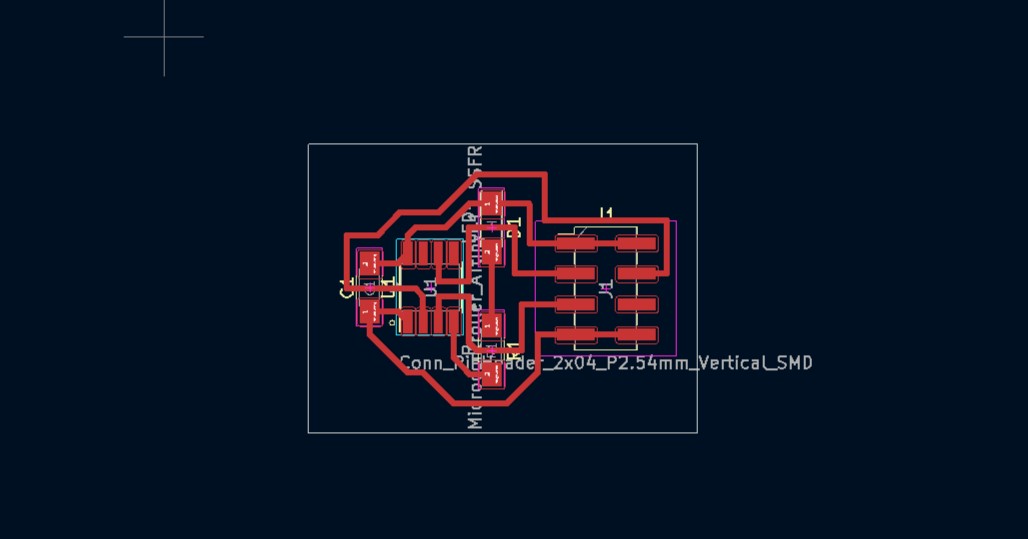
After designing my schematic, I started to design my PCB. This was also easy and I followed my Week 5 which shows me how to make a PCB design.
This is what it looked like:
PCB for Node Board
Next, I needed to design my Parent Board.
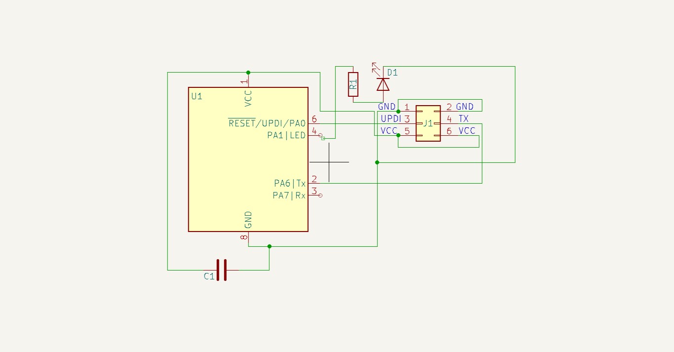
To design my parent board I did the same thing as I did for my node board.
Schemtic for Parent board
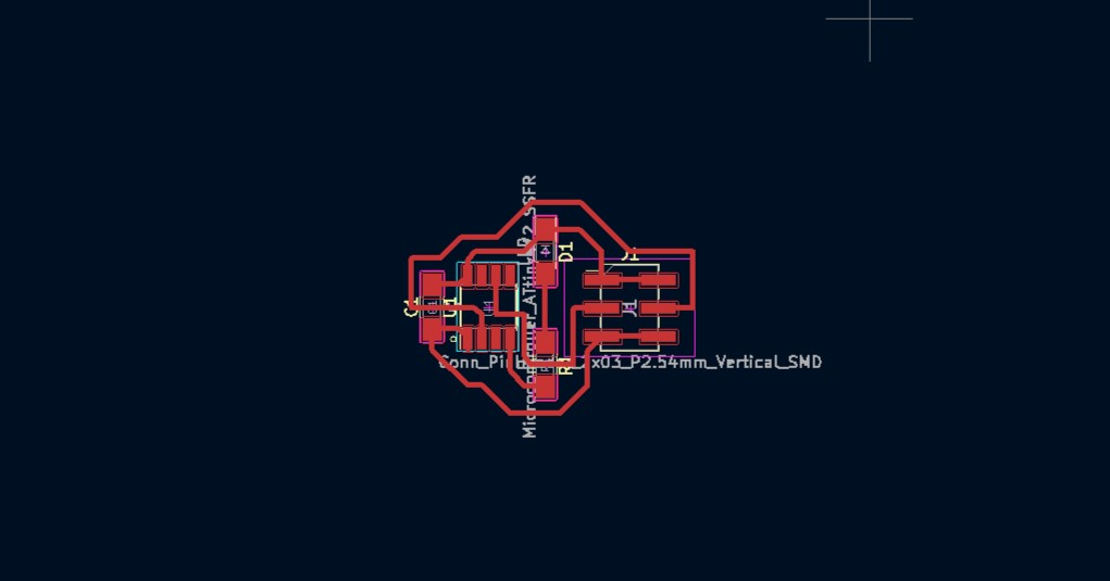
After designing my schematic, I started to design my PCB. This was also easy and I followed my Week 5 which shows me how to make a PCB design.
PCB for Parent board
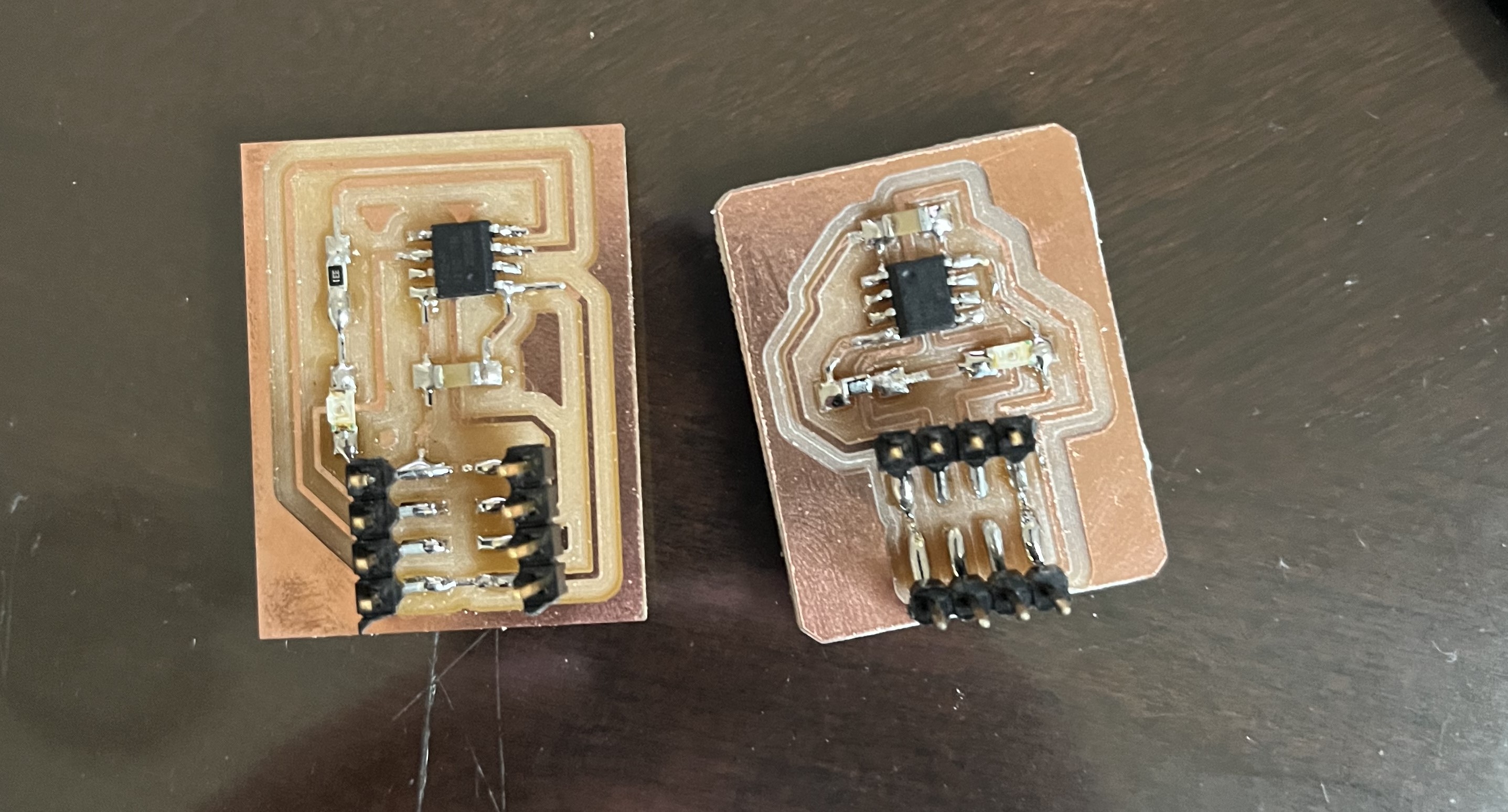
Once all the PCB and Schematics were designed, I decided to mill my boards. This was easy as I have done this many times before. I followed my Week 5 documentation and started to mill my boards.
Here is a video of my milling my board.
After milling, I soldered all the components on my board and was ready to start programming them.
Programming
To program my boards I first had to upload some code to each chip this is so the boards would understand their “id”. So when called upon by the Parent board the boards would know what id/ Number they are assigned to.
In my case, I have 2 boards. One parent board and one child board. The parent board will send out a signal to the node board, and then the node board is expected to receive that signal from the parent board. This is done through RX/TX. You can see this done and all the components connected to my PCBs.
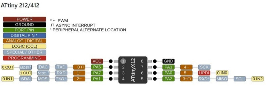
To easily refer to this, check out the AtTiny 412 pinouts.
AtTiny 412 Pinouts
But before I started assigning g these board codes, I wanted to test if each of them received a simple blink code. To do this, I opened a simple blink code in Arduino IDE and programmed my parent board with that.
This is the code I used:
Simple Blink Code
void setup() {
  // initialize digital pin LED_BUILTIN as an output.
  pinMode(2, OUTPUT);
}

// the loop function runs over and over again forever
void loop() {
  digitalWrite(2, HIGH);   // turn the LED on (HIGH is the voltage level)
  delay(1000);                       // wait for a second
  digitalWrite(2, LOW);    // turn the LED off by making the voltage LOW
  delay(1000);                       // wait for a second
}
Video of Parent Board Working
After testing this, I assigned each of my boards with their respective codes.
Here is the code for the Parent Board.
Code for Parent Board
const int ledPin = 2; //Pin # of LED

void setup() {
  Serial.begin(9600);
  pinMode(ledPin, OUTPUT);
}

void loop() {
  delay(2000);
  Activate();
  Serial.print(0, DEC);
}

void Activate(){
  digitalWrite(ledPin, HIGH);
  delay(500);
  digitalWrite(ledPin, LOW);
}
Then I uploaded the code to the node board.
Code for Parent Board
int inByte = 0; //Recieved Byte
const int id = 0; //Local Node ID
const int ledPin = 2; //Pin # of LED

void setup() {
  Serial.begin(9600);
  pinMode(ledPin, OUTPUT);
}

void loop() {
  if (Serial.available() > 0) {
    inByte = Serial.read();

    if (id == inByte){
      Activate();
    }
    else{
      Serial.print(inByte, DEC);
    }
  }
}

void Activate(){
  digitalWrite(ledPin, HIGH);
  delay(500);
  digitalWrite(ledPin, LOW);
}
Once these codes were uploaded, I wired both my boards together as shown. I followed my schematic to avoid any mistakes. I then Uploaded this code. This code was the conjointment of both.]
Conjointment of Both Codes
int inByte = 0; //Recieved Byte
const int id = 0; //Local Node ID
const int ledPin = 2; //Pin # of LED

void setup() {
  Serial.begin(9600);
  pinMode(ledPin, OUTPUT);
  Activate();
}

void loop() {
  while (Serial.available()==0);
  int incoming = Serial.parseInt();
  if (incoming == id){
    Activate();
    delay(500);
  }
  else{
    Serial.print(incoming);
  }
}

void Activate(){
  digitalWrite(ledPin, HIGH);
  delay(500);
  digitalWrite(ledPin, LOW);
}
Once conjoin ing these two codes, I uploaded the program and… IT WORKED!!!
Here is a video of my networking working!!
Final Networking Working
Demonstration
These were my files for this week.
Week Summary
Overall this week was great! I learned how to network two LEDs together as well as learning to do actual networking and communicating. This helped for my final project and I am glad this wee was included in Fab
Group Work
Link to group site!
For this week’s group work I worked with Andrew, and Aarush to network 2 Ardunios together. I learned a lot about networking, as well as learned about SCL and SDA communicating between 2 Asrdunios. TO learn more about our group project, check out this link.