5. Electronics production
Assignment: Make an Incircit Programmer with A Microcontroller
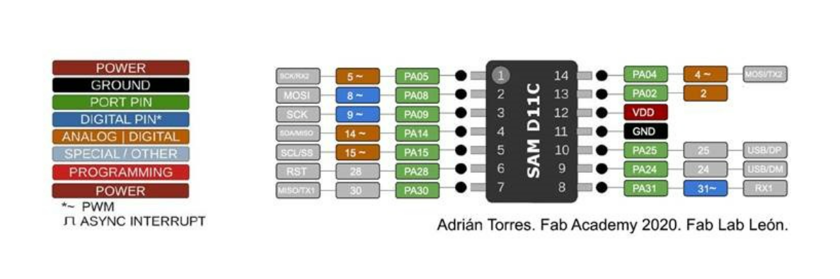
I made a SAM Programmer, which is used as a programmer or USB/UART.
I used Adam Harris’s Website on how to make this board. Mr. Harris’s design was straightforward.
This was one of the most complicated assignments which I had encountered so far. I have never milled or designed a PCB board before, so this was all very new to me. Mr. Haris broke the process of how to make a SAM programmer into 4 steps.
These are my files for the week.
Steps:
- Download the board files and code.
- Mill the PCB with Roland or another CNC
- Populate (stuff) the board with components ( sodering)
- Flash firmware to the chip
- Use this new board as a programmer or USB/UART
I first started with the first step which was to download Mr. Harris’s files onto the lab’s computer. I would then open the files into Bantam Tools and follow a specific workflow.
Mr. Dubick my instructor posted the files and the schematics on to Google Classroom.
Schematic On How To Assemble Board.
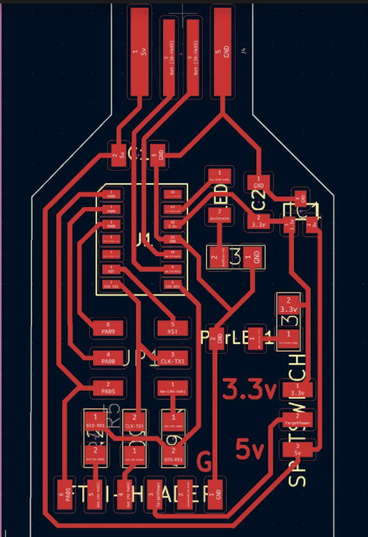
After downloading the .gtl file, and opening it into Bantam Tools, I follow this workflow, which was made by Mr. Dubick.
Milling on Bantam Tools Workflow
Fail #1 of PCB Board
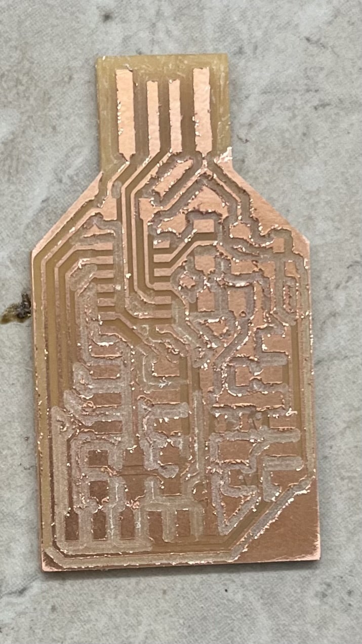
After following this workflow successfully, I realized that the traces were too thin and checked them under a microscope, and saw that many of the traces had ripped. This was a bummer, so I went back and checked what bit I used and compared my board with the other boards of my colleagues. Many of them had used the 0.005 PCB Engraving Bit. In this first print of the board, I ran into many challenges with choosing the bits. This is because the bits in the lab were misplaced, and I could not tell them apart. I was working under the assumption that the engraving bit was a 15-degree Flute Taper Sub. I correctly assembled and got my milling settings ready by following the workflow above, although milled the board with the 15 degrees Flute Taper Sub. BIG MISTAKE!!! I then realized that I was using the wrong bit because I compared it with my classmates. I changed the bit to a 0.005 PCB Engraving Bit. After following the workflow again, I finally milled out the correct board. I was a little frustrated during this process, although I have to remember that mistakes happen and I shouldn’t be too hard on myself. Milling the board taught me patience, organization, and effectiveness.
Process:
Result:
Settings:
| Test Try | Bit 1 | Bit 2 | Result | Solution |
|---|---|---|---|---|
| Fail #1 | 1/32 in Flat End Mill | 15 degrees Flute Taper Sub | Narrow traces | Changed bit |
Fail #2 of PCB Board
I went back and changed my bit from a 15 degrees Flute Taper Sub to PCB Engraving Bit 0.005. The difference between them is that the 15 degrees Flute Taper Sub has a more narrow V-shape to its tip, unlike the 0.005 PCB Engraving Bit, which has a wider V-shaped tip. I decided to use the PCB Engraving Bit 0.005 as it would help me make wider traces, so they wouldn’t rip. Although I learned that this did not work, I was one step closer to the PCB board I desired. I still kept all the settings to normal and followed the workflow. Usually, I would have more patience than this, although this process was becoming very frustrating. I had to mill the third board, although this time I spoke to Mr. Harris and Mr. Dubick and they told me about adjusting the trace depth and trace clearance.
What Is Trace Depth And Clearance
Trace Depth- Trace depth is the distance in the z-axis that the end mill will cut, so if the distance is changed, the bit can become too big or too small to engrave onto the board.
Trace Clearance- Trace Clearance is how much of the unnecessary copper on the board should be removed. This makes the board look neater and makes it easier to solder.
Result:
Settings:
| Test Try | Bit 1 | Bit 2 | Result | Solution |
|---|---|---|---|---|
| Fail #2 | 1/32 in Flat End Mill | 0.005 PCB Engraving Bit | Narrow traces | Changed milling bit and adjusted tace depth and clearance |
Success!! (without visual appeal)
After speaking with Mr. Harris, he suggested that we change the trace depth and clearance. When making the ATiny 412 chip Mr. Dubick had shown my colleagues and me how to customize the trace depth and clearance. After processing this information, asking questions, and googling. I changed the trace depth and clearance depth to 0.1 to see if there were any live changes made on the preview screen, but there wasn’t much difference. I then changed the number to 0.2, and barely saw a change. Although, Mr. Harris agreed that this should work. Then I realized that the reason some of the traces were being so thin was due to many factors such as trace depth, trace clearance, and the bit size. The whole time I was ignoring the fact that I had a 1/32 inch Flat End Mill bit, but there was a 1/64in Flat End Mill Bit in the lab!! How could have I have missed it!! I changed the settings for the order in which the bits would cut.
Bit Jobs:
- 1/64in Flat End Mill Bit was to cut out the traces, so they weren’t too thin.
- 0.005 Engraving Bit was used to engrave the PCB
- 1/31 inch Flat End Mill Bit was to go over the traces the 0.005 Engraving Bit could not go over. After making these changes I milled out the board and it worked!!
Result:
Settings:
| Test Try | Bit 1 | Bit 2 | Bit 3 | Result | Solution |
|---|---|---|---|---|---|
| Success!! (without visual appeal) | 1/64 in Flat End Mill | 1/32 inch Flat End Mill | PCB Engraving Bit 0.005 | More copper around the PBC | Adjusted tace depth and clearance |
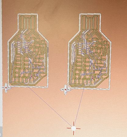
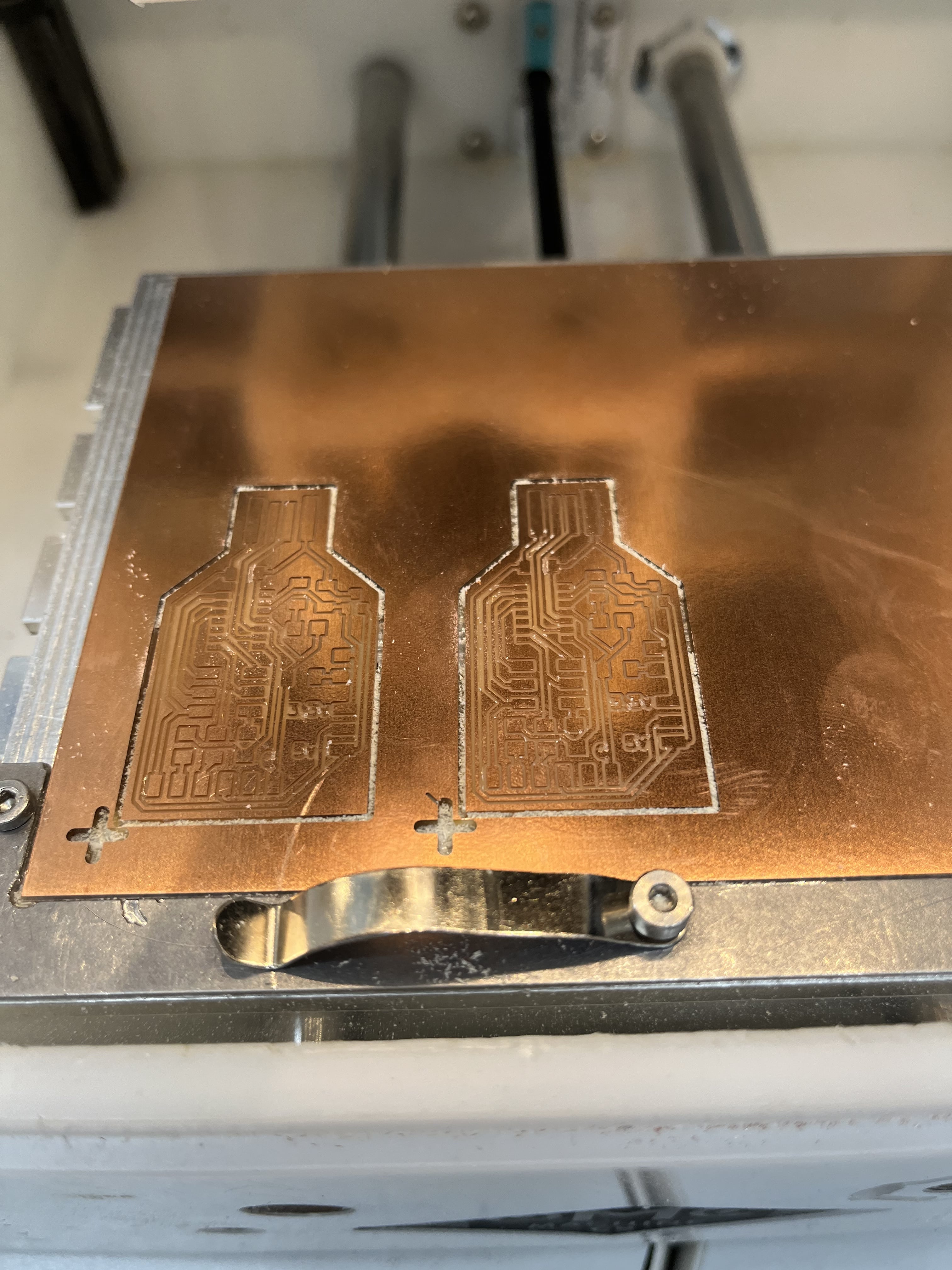
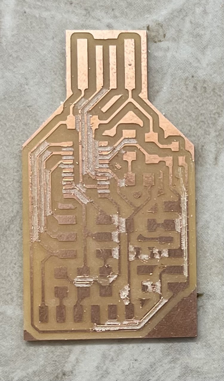
Final PCB Board (Until it got messed up)
After making all the changes with the three different bits, I adjusted the trace depth and clearance to 1mm. The reason I chose three different bits, was because each of them had different jobs to do.
After organizing what order the bits are going to be used in the machine software, Bantam Tools, I made sure that I followed the Workflow and began milling the PCB board.
I followed the post process on how to remove the board carefully and examined all the traces, finding any which may be broken. Thankfully there were none. The PCB board also looked MUCH cleaner, and it was 10x easier to solder.
Result:
Settings:
| Final Result | Bit 1 | Bit 2 | Bit 3 | Result |
|---|---|---|---|---|
| Final PCB | 1/64 in Flat End Mill | 1/32 inch Flat End Mill | 0.005 PCB Engraving Bit | Soderable PCB and happy Fab Student |
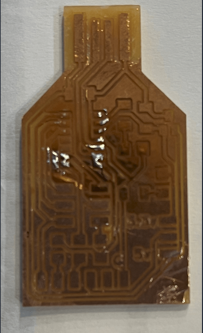
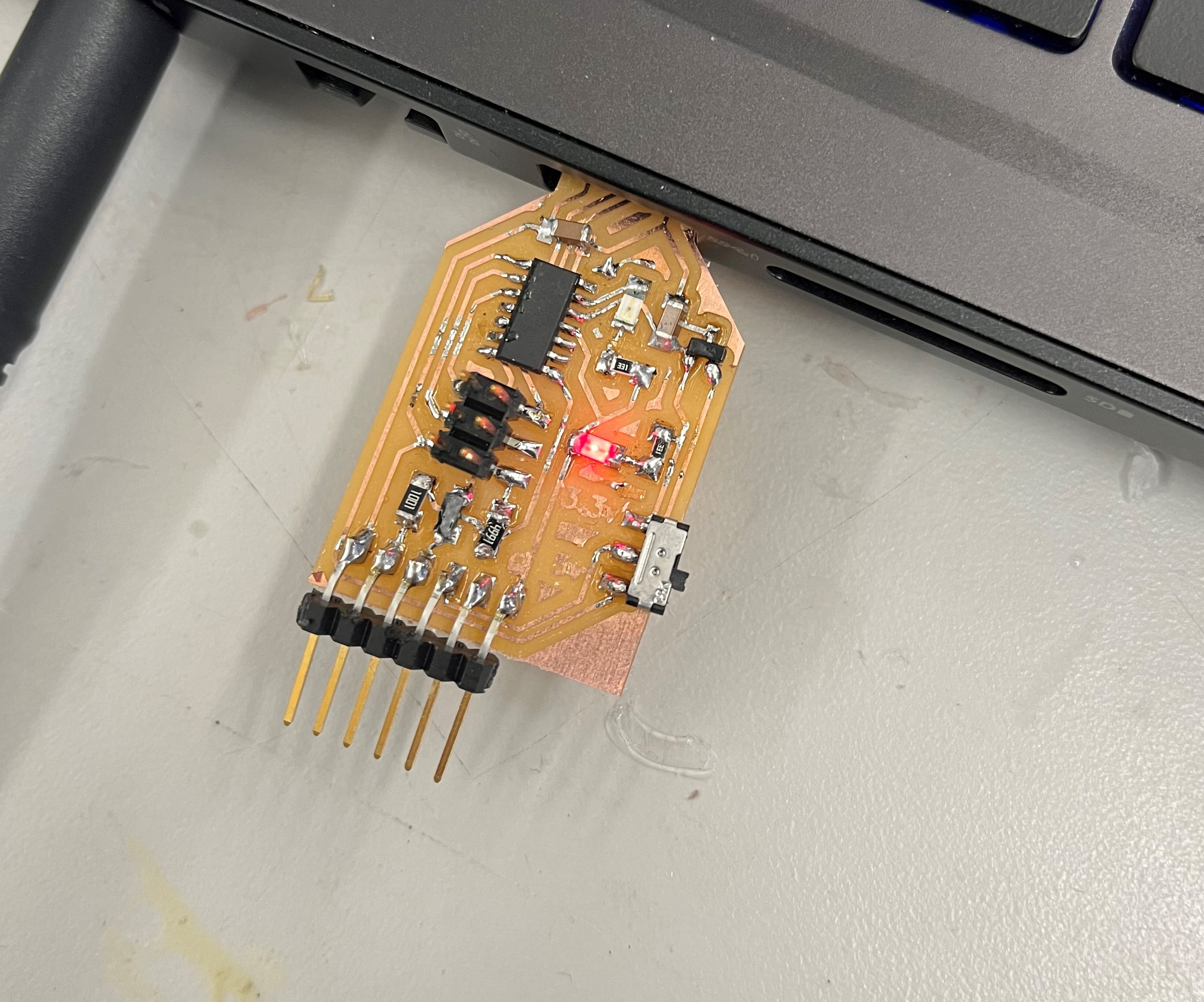
Soldering Board
Sodering the board was very straight forward although it is not one of my strengths. I had a very hard time sodering the SAMD11 chip because the pins and pans of the chip and board were so close. My hands kept on shaking and kept moving the board. Observing my other colleges, I got the idea to tape down my board and to solder it that way. This was MUCH easier to do because the board wasn’t moving around. To steady my hand shaking from so much I would place a dot of solder on one pad, and then use tweezers to hold the component in pace and use the soldering iron in my dominant hand (right hand) and get the component to stick on the board. Then with ease, I would place solder on the other pins/ sides of the components and hold my other hand stead while making the final adjustments to the component. While sodering the components on, I had to be VERY careful not to rip any traces. I did not realize that traces were so delicate, although the soldering board taught me to be gentle with my materials.
After sodering the board I had to use an exact-o knife and trim some copper of the part of the board. This is so it does not break the USB port and stop it from working on my computer. I carefully trimmed the copper on the edges of the board, and make sure not to rip any traces while doing this process. I should have trimmed the copper before stuffing the board with the components because this made it hard to trim the copper, as also posed a major threat to me ripping a component or a trace. Thankfully that did not happen and it was successful.

To make sure all my sodering was done right, I plugged the PCB board into my computer and make sure it had power. The red LED turned on, which indicated that I had power and my board was working. I was so excited because I had spent so much time soldering all the components to this board.
Software
Following Dr. Harris’s Website I started to get my board ready to program and to
upload the code and make my board into a USB. This was probably the hardest step, as I had to use the Atmel- ICE. An ATMEL-ICE is a debugger that would help load the software onto the PCB Board.
In order to upload the software, you will first need to download some files! First, make a folder where these files will reside. I named mine “SAMD11 Board Files”.
Then download the following files:
This file is a debugger tool that we will use to helo us download the firmware onto our device.
SAMD11C Arduino Bootloader Core Firmware
This is so we can access the chips and libraries with the Arduino IDE.
Free-DAP firmware This will come in handy later when we use this board to program other SAMD chips.
Once you have downloaded all these files and located them in the same folder. Open your Command Prompt as an ADMINISTRATOR and then run the following code:
remember to change the “24” with the number of the version you downloaded.
Once running this command you should get this message:
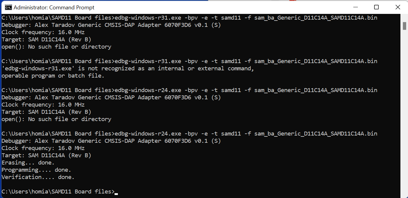
After all, this is done your program should be uploaded to your board. Although this was NOT the case for me.
After HOURS AND HOURS of trying to figure out what the problem was, I finally realized that the ATEML- ICE was broken!! Before I realized that the ATMEL- ICE was broken, I tried to pinpoints the components that could have been bad or not sodered on properly on my board. One of the resistors had a bridge with one of the traces, which I had noticed. I tried to unsolder the bridge, but I ended up ripping the trace. I was VERY frustrated and angry, although Mr. Dubick told me that I could use solder and bridge the trace back together. I searched for a tutorial on how to do that and saw some ways to do it. I try to mimic how it was done, and it surprisingly worked. I used a multimeter to check the current and I got a little beep sound which indicated that there was power.
After doing this, I went back and used the ATMEL-ICE again, although it still did not work. This was very frustrating so I went back and checked the sodering job on it again. All of it was right, so what could have been the problem. I wish I had known that the ATMEL - ICE did not work because I wasted a lot of my time on that.
That night I decided to use one of the spare boards I had and restart the process and solder all the components on again. The chip again was the hardest to solder, but it still worked. I finished soldering all the components making sure all of them were in the right place and the right direction, and then I tested it out with Dr. Harris’s Board.
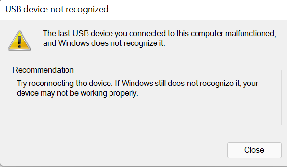
When I plugged in the board, the power LED lit up, signifying that the board had power and there were no traces ripped. That was a MAJOR relief. After plugging in the SAMD11 PCB board the computer gave me an error saying: “USB Device Not Recognized”. That was strange, what could that mean? Mr. Dubick told me that it could mean that something id shorting my board and that I should either check my sodering working to find any bridges or see if any pieces of copper and loose and touching other traces.
In the microscope, I checked to see whether or not my sodering work was right. Thankfully it was. Then, I checked to find loose pieces of copper. I used an Exacto knife and tweezers to find pieces. I found a couple of loose pieces of copper. I scarped them out carefully making sure not to rip any traces, and then when to test the board again. When I plugged the4 SAMD11 chip into the computer, the computer gave me the same error. I could not pinpoint what it was. This was EXTREMELY stressful and frustrating. I was running out of time and I still did not have a functioning board. To fix this Dr. Harris recommended that I check the USB/DP pin (pin #10) and the USB/DM pin (pin #9) to see if I could add more solder onto them. I added a little solder and went back to check, still no success.
I took all my old boards and showed them to Dr. Harris and he recommended that I upload the software to one of my old boards and then switch the chips on them by unsoldering them. I did exactly that. First I uploaded the code to one of the old chips by running the commands described above and then took the heat gun and unsoldered that chip. I also unsoldered the current chip which was on my board and then came to realize that there was NO solder on the USB/DP pin (pin #10). I was in utter shock that I did all this work just to find that out. To justify this stupidity on my part, it was very late in the night around 10:30 pm when I was in the lab figuring this out.
With all this in mind, I quickly went to get another chip from the materials box, and started sodering that chip triple checking that I have solder on EVERY SINGLE pin. I even double checked by using a multimeter to see if the pins had current. I also used the mulitmeter and mesured the current on Dr. Harris’s board to make sure that the currents in his board match mine. THEY FINALLY DID!!!
After double checking all this, I was ready for success. I plugged in the SAMD11 chip into my computer and SUCESS!!!! I was so happy and exicted!! After not reciving a message from the computer, I was sure that the SAMD11 chip was registering as a USB.
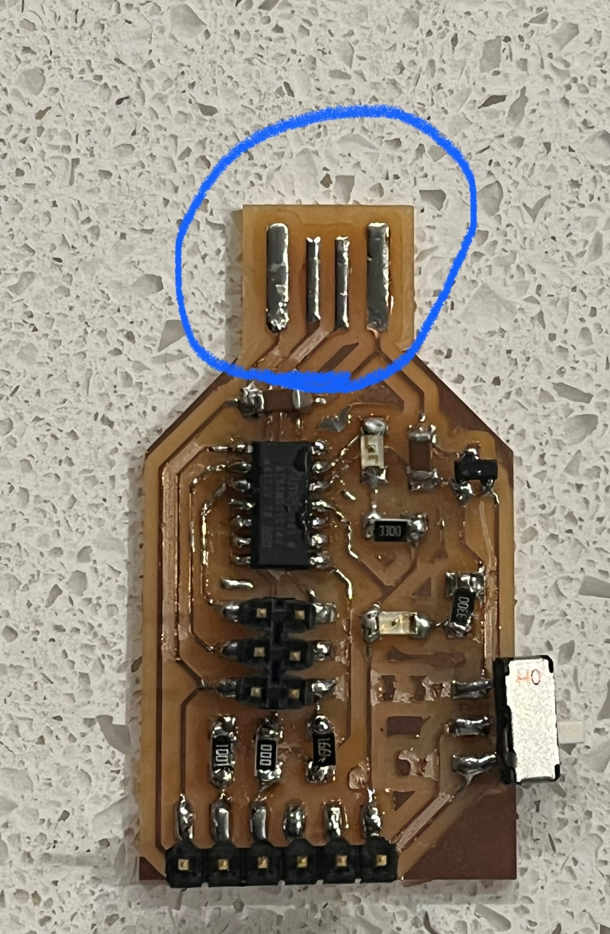
My chip kept wiggling in the USB Port and I would have to hold it up with my finger, so to get rid of the inconvience, I decided to solder the part of the PCB which goes into the port. I sodered the 4 strips and solved the problem. The PCB stayed in place and I did not have to support it with my finger anymore.
Software For Final Board
I plugged the SAMD11 Chip into the computer and ran the code:
rember to change the “24” with the number of the version you downloaded.
Once running this command you should get this message:
Now all the programs are uploaded to your SAMD11 chip!
This lets Arduino program the chip via USB.
Blinky Test
- Open the Arudio IDE
-
In the software, go to File → Preferences→ Additional Boards. Paste the following:
https://www.mattairtech.com/software/arduino/package_MattairTech_index.json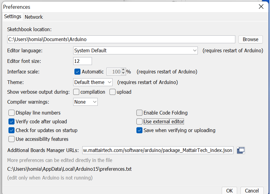
-
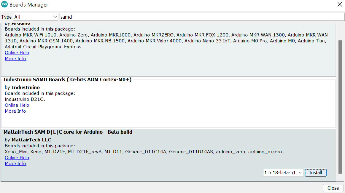
Next, you need to install the SAMD boards. Go to the top navigation bar and go to Tools → Boards → Board manager. In board manager, search for “SAMD” and install the “MattairTech”.
-
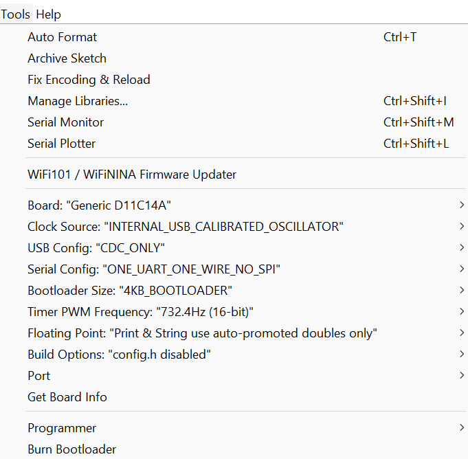
Make sure you are using the correct board, port, clocksource etc:
Make sure to have “INTERNAL_USB_CALIBRATED_OSCILLATOR” when you plan to keep this plugged into the USB port for power.
-
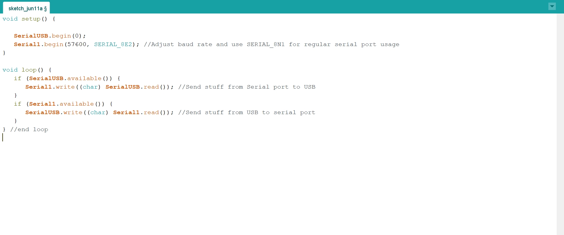
Write the code for the chip You can copy/paste this one: I chose to write a code wich printed the word “hello” infinelety, I used the serial monitor to see the results. I did not choose to blink my LED because it was sodered on the wrong way, and I was recommended not to desoder it because I may mess up my board.
void setup() {

   SerialUSB.begin(0);
   Serial1.begin(57600, SERIAL_8E2); //Adjust baud rate and use SERIAL_8N1 for regular serial port usage
}

void loop() {
   if (SerialUSB.available()) {
      Serial1.write((char) SerialUSB.read()); //Send stuff from Serial port to USB
   }
   if (Serial1.available()) {
      SerialUSB.write((char) Serial1.read()); //Send stuff from USB to serial port
   }
} //end loop
6 . Run the code and voila!! Your SAMD11 Chip is programmed and ready to use and now is a Programmer!
Program the Board as a UPDI
Previously I had made a Attiny Board and so I used that to get it programed over a UPDI.
Here are the steps I used to program the board over a UPDI.
-
First, you want to get a Attiny board. (This was already milled by Mr. Dubick) These are the steps Dr. Harris used.
-
Use the Blinky Test Code above. This will make your Attiny’s LED blink.
-
Change your chip to an attiny412 in the Arduino IDE.
This is SUPER important becausd if you dont, then your SAMD11 chip will be reprogramed.
-
Next, change the “programmer” to “SerialUPDI – SLOQ: 57600 baud, any platform…”
-
Wire up the Board as shown below.
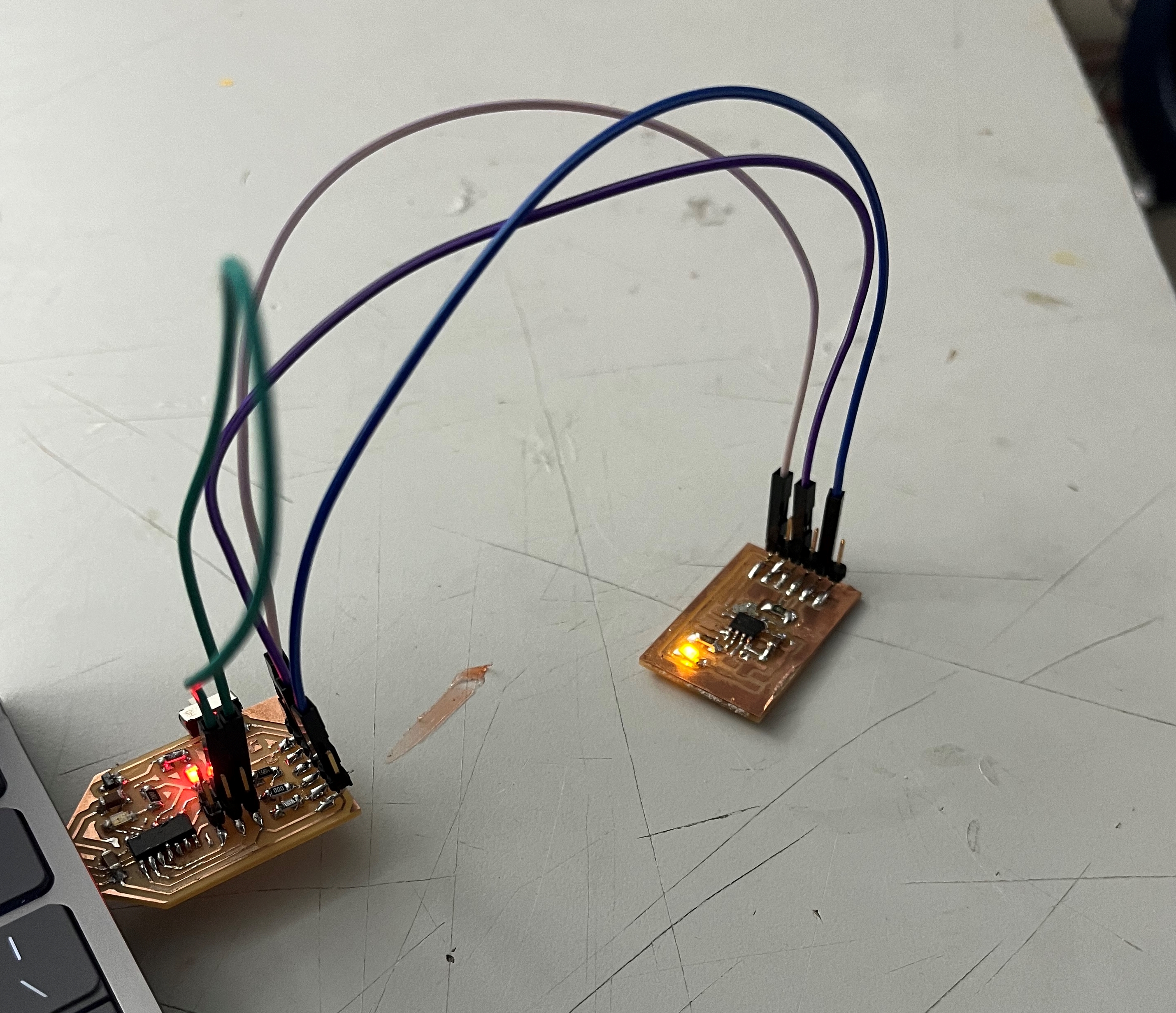
6 . Success!!
Summary
This week I learned how to mill a PCB Board and learned how to use the Bantam Tools Milling Machine. This week was by far the hardest week, as I have never done this skill before. Although, as I watched Youtube videos and learned by watching people, I became better. I noticed that with every board I milled I became more efficient and faster. By the last board, I finished milling and sodering in less than an hour. Whereas my first board took me more than an hour. Software and programming are not my forte, although I learned that with patience and a good base foundation to concepts it becomes straightforward. Throughout this process, I noticed that the more mistakes I made in the begging, the more I would have to fix them in the end. So the moral of the story is to do a good job at first by not rushing, and then everything else will fall into place.
Group Work
This week, we had to characterize the design rules for our in-house PCB production process. This was a very simple week. The entire student group did this process, so it went quickly and smoothly. Here is our group site