6. Electronics design
During this week, I worked on redrawing an echo hello-world board and adding a button and an LED. While doing so, I was also tasked with checking the design rules of the board, making the board itself, and making sure it can communicate
Prior Ki-Cad Work
Before the official start of Fab Academy, our instructors provided us with resources to learn all about KiCad, the software suite for electronic design automation that we were going to use, in order to prepare ourselves for this week. We were given the Tech Explorations course in order to learn KiCad. Through this course, I learned all about the basics of KiCad and was a great head start into the week.
Starting Design Work
Schematic Design
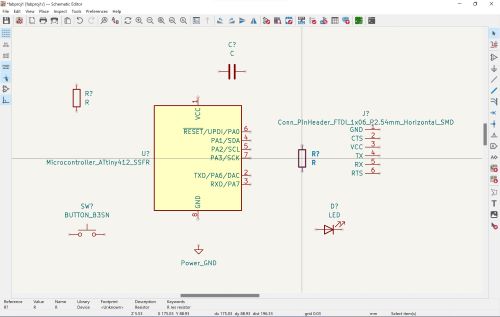
This week was similar to past weeks in that we were to mill and program a board through a programmer, but it was far more difficult since we were tasked with developing our own boards. I started by downloading the Fab Library onto KiCad and making sure it worked. I then opened a new KiCad project and began designing my board. I started by placing the ATTiny 412 board and a three pin header onto the schematic.
Then, looking at the designs of Mr. Dubick and Dr. Harris, I started designing the rest of my board.
Some of the other components I used were: - Unpolarized Capacitor - Resistor - LED - 4 Pin Button
I added tracks and organized my layout
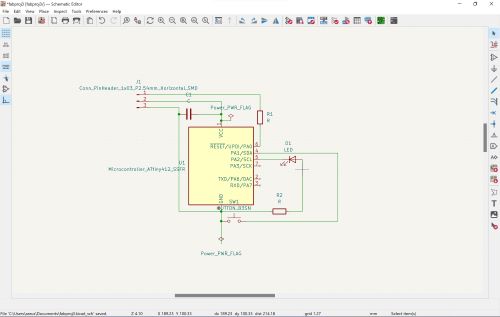
On my design, you can also see that I have placed some things called power flags, which act as power or grounds to have the schematic run properly.
Mr. Dubick also told us to use the symbol editor to label unused pins as disconnected in order to reduce the number of errors that would pop-up when I ran the electrical rules checker(ERC) that checked my schematic.
Doing this would also specify each individual component, as you can see with the labels in the picture above. For example, teh two resistors are differentiated with R1 and R2.
After I did this, I ran the ERC on my design to see if I was ready to move on to the next step, but I was given list of 16 errors
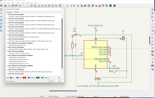
I went throught the errors and saw that they were all mostly the same, saying the pins of my components were not connected or the wires were not connected. I zoomed in on my design and saw that they indeed were not connected. I realized this was an error due to the grid size and snapping of the document I was working with, so I restarted my design on a page with thicker grids and that the components could snap to better.
After I did this, I ran the ERC again, and this time it was successful.
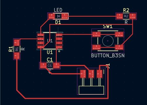
I saved this schematic and uploaded it into the PCB editor part of Kicad.
PCB Editor
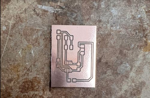
The PCB editor part of Kicad was sort of like a puzzle, and completly a pain. I had to connect the correct wires/traces to the different components that could be connected, but I had to do this without the the wires/traces overlapping or be too close together. Having traces too close to each other would result in an increased opportunity for solder bridges. I was also told to make the trace thickness atleast 0.4, so I made it 0.5.
When I finially finished, my board looked like a mess. I was scared it wouldn’t work becasue it has traces going thorugh other components, but Dr. Harris said it is okay.
The design rules checker of the PCB Editor had warnings about silkboards but the machines in our lab did not use silkboards so I was ready to export my file.

Exporting Files
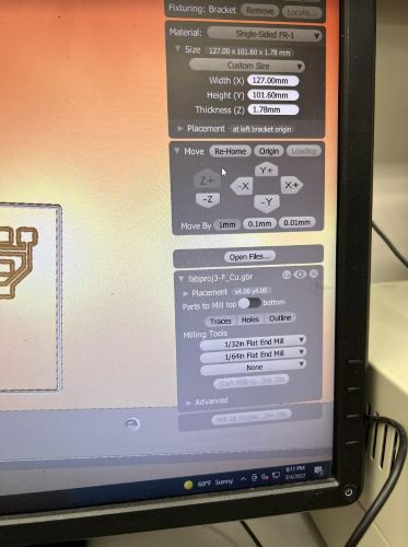
In order to print, I had to export the gerber files. To get these, I went to file > plot. Next, I unchecked everything except the F.Cu and Edge.Cuts since that that is all I needed.

I was finally ready to start milling.
Milling and Populating Button Board
I uploaded the files onto the Bantam CNC software in our lab, followed the previous documentation I had made for milling, and started the job.

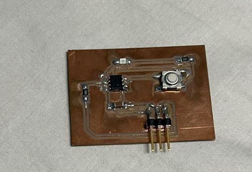
After I milled my board, I populated it with all the components I used in my schematic
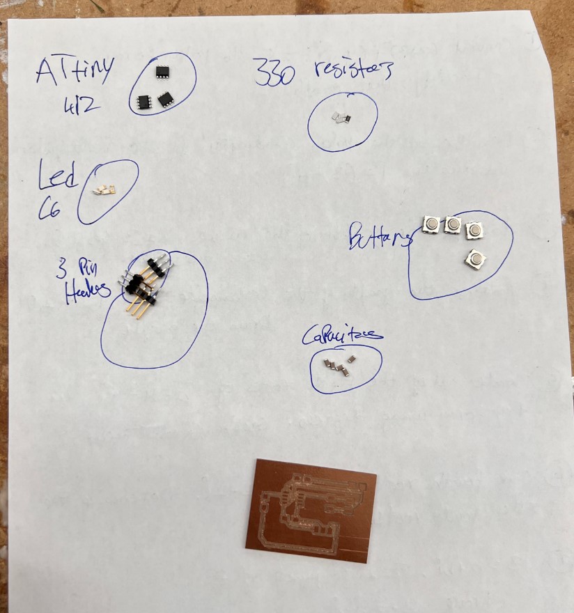
By now, I have had a lot of experience soldering so this task didn’t take much time at all.
Programming Button Board
After I had my finished board, my next step was to program it to work as a blink board. Given this task, I was not allowed to use the button as a kill switch which made it a bit harder.
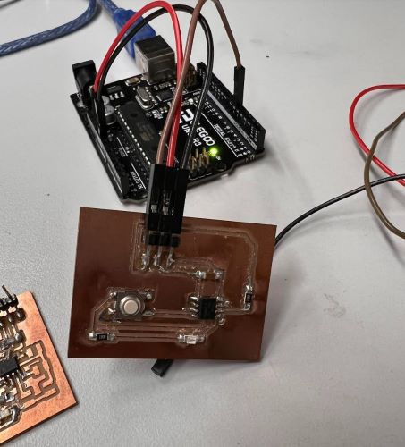
I initially tried to program my button board using my SAMD11C programmer I made in week 4. I configured the settings in the arduino IDE to use the SAMD board as a programmer, and compiled the code. However, I was not able to send the code through. I asked Dr. Harris, the designer of that specific SAMD programmer board why the code wasn’t being sent through, and he explained that the SAMD chip is faulty and sometmes doesn’t work. Due to this, I decided to use my Arduino Uno.
Following my prior documentation, I configured an Arduino with jtag as a programmer. I wired up my board, changed the board and the programmer to the correct settings, and sent this code through.
int ledPin = 1;

void setup()
{
    pinMode(ledPin, OUTPUT);  // Defines the LED pin
    pinMode(4, INPUT_PULLUP); // Makes the button pin read as HIGH if button isn't pushed
}

void loop()
{
    if (digitalRead(4) == HIGH) // Button Isn't Pushed
    {
        digitalWrite(ledPin, LOW); // LED will stay on
    }
    else
    {
        digitalWrite(ledPin, HIGH); // LED turns off
    }
}
My board worked first try!
I was surprised I was able to get it to work so quickly, but was quick to get a video as well just incase something happened.
What I learned
Through this week, I learned about the entire PCB design process. I had previously milled many PCB’s, but never had designed a single one, so my assignment this week marked the first board I designed and milled. It was a thrill when the board I designed from a concept came into frutation and worked. The design process was arduous but with more practice, I can become proficient with it.
Group Assignment
In addition to our individual projects, we were assigned a group task this week. The assignment was to make use of the labs resources and learn how to work with oscilloscope and a multimeter. I had used multimeters many times before, but never used an osciloscope. I also learned about the similarities, differences, and advantage of both tools. This week, we tested voltage and diodes on an ATtiny 412 board we made. You can find our work here
You can find my files for this week here