Week 13. Input Devices (Apr 12)
Week 13 Assignment
- measure something: add a sensor to a microcontroller board that you have designed and read it
Joystick Reader
For this week, our assignment was to add a sensor to a microcontroller board and read its output. At the beginning of the week, I had many ideas of sensors I could do, and I had no idea which one would be best. I wanted something that would both contribute greatly to my final project, but also could be built upon in the networking and interfacing weeks, so my effort wouldn’t be wasted and I wouldn’t have to restart for those weeks seperately.
I began looking at sites and thinking about how this week could fit into my final project. Here are a few that I looked at: Site 1, Site 2, Site 3
After talking with Dr. Harris, I narrowed my input week ideas down to two options, each with some contributing value for my final project. I could either make
-
a joystick board capable of wirelessly transmitting information through radio
-
a prototype flight controller board based off of neil’s accelerometer, gyroscope, magnetometer sensor board.
I decided to go for the first option based on the fact that I had already figured out which radio I was going to use: the nRF24l01 tranceiver module, which I talk about more in networking week. My goal for this week only, was to mill a board capable of reading joystick values and printing them onto the serial monitor.
Note: Originally, I wanted to get a head start on networking by sending over the joystick values through the radio board to another Arduino, but time constraints ended up preventing me from this further goal
Iteration 1: Modified Satshakit V1
During the talk with Dr. Harris, he mentioned that if I wanted this to be a prototype for my final board, I should use an Atmega328p chip instead of the normal Attiny chips I had used before. He explained this was because in order to control 4 motors at the same time, I would need to send a PPM signal instead of a simple PWM signal. The ATmega328p chip was one of the only Atmel chips in our lab that could generate a PPM signal, so that’s what I thought I needed at first.
After coming up with the idea and doing research, I then moved to PCB design. Within my research, I noticed the frequency of Arduino Nanos being used with the nRF24l01 when doing research, so I thought that I could make my own Nano at first. I found this site to help with that, and took the Eagle Schematic and PCB design and imported it into KiCAD
Initial schematic of the nano
Initial PCB design of the nano
As you can see, the blue traces are the ones on the back side, and the red traces are on the front side. Because this involves double sided milling, I decided not to do this option. I am not familiar with double sided milling and I didn’t want to create unnecessary trouble.
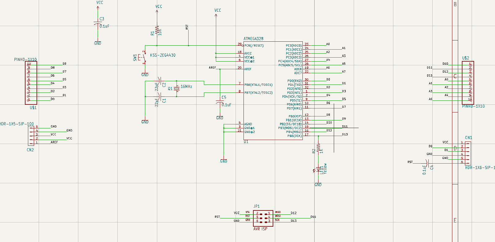
Then I began looking for other options to the Fabduino, when I stumbled upon the satshakit. The satshakit is a completely fabbable board that resembles an arduino uno, and it uses an ATMega328p chip, so I thought it would be perfect for me to make one. After getting it confirmed by Dr. Harris that this was indeed a good option, I once again took the Eagle Schematic and PCB design files linked on the satshakit page and imported them into KiCAD
Here is the schematic which is unmodified
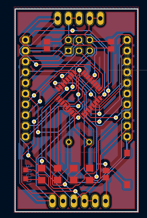
This is the unmodified PCB design for the Satchakit. I didn’t really enjoy the look of the through hole headers, and I soon realized that I didn’t need all the pins. Plus, I needed two extra ground and VCC headers for the joystick and nRF tranceiver I would be adding. I made these changes and ended up with this design, and then went to go mill.
Again I followed the same process of milling that I normally do. For more information about milling check out Week 05 Electronics Production or Week 07 Electronics Design. Here I include three videos for the location of the three tools, the PCB 0.005, 1/64, and 1/32 flat end mills
PCB 0.005 Engraving
1/64 end mill
1/32 end mill
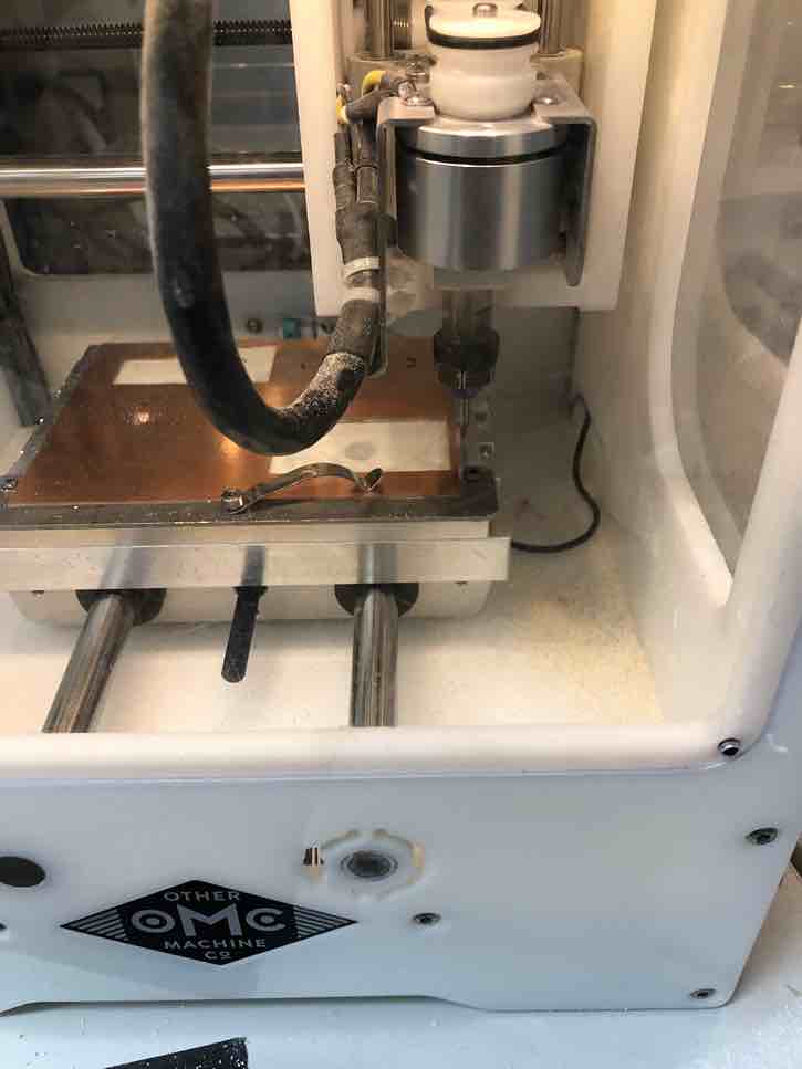
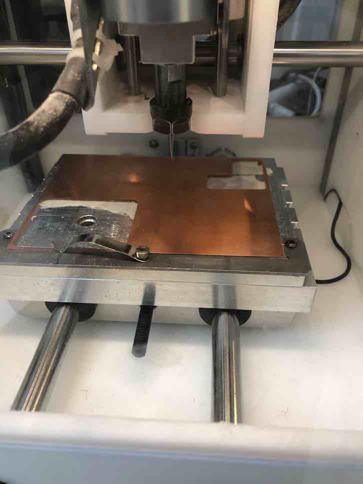
The milling went pretty well, and after it was done I just used the vacuum to suck up all the excess copper. Then I rinsed the boards under water to clean the surface of the board from tiny sprigs of copper stuck to the traces. After milling out the board I populated it with these components
-
1x Atmega328p-AU
-
2x 22pF capacitors
-
1x 16 MHz crystal oscillator
-
Vertical SMD headers
-
2x green LEDs (our lab didn’t have yellow ones so I swapped them with green)
-
2x 499 ohm resistors
-
2x 100nF capacitors
-
1x 1uF capacitor
-
1x 10uF capacitor
-
1x pushbutton
-
1x 10k ohm resistor
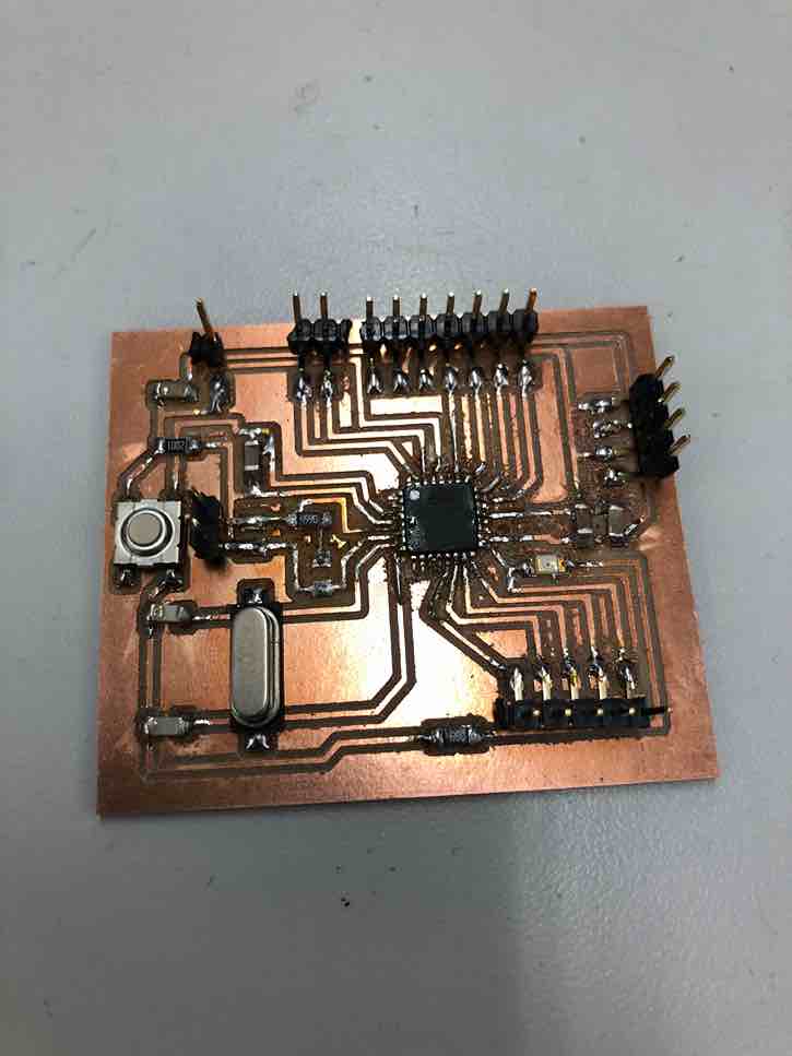
The soldered board turned out pretty nicely, and it looked like this. I would say that my soldering skill has definitely improved from the previous weeks, but there are still a few rough spots around the chip since its legs are so close together and I had to wick off a few solder bridges.
Once I had it soldered the next step was to test and see if it got power. I used an Arduino, and simply just plugged in the VCC and GND pins of the board to 5V and GND of the Arduino. To my surprise the green LED lit up, indicating that the board did receive power.
Next I checked back on the satshakit github page, and figured out that I had to burn the bootloader. I intended to do this through ISP, by first turning the Arduino into an ISP programmer and then programming the board through the Arduino. Something I’ve noticed is that this concept of first turning something into a programmer and then using it to progam and target board seems to be a fundamental pattern in embedded systems, not only in ISP but UPDI as well. The reason I had to burn the bootloader and couldn’t just program the satsha through ISP is because this step would essentially make the satshakit programmable through only a serial to usb connection, just like an arduino. This would eliminate the need for the Arduino ISP programmer and I would only need a serial to FTDI converter
Here are the steps I intended to take to upload the Arduino bootloader
-
open Arduino IDE
-
select proper programmer (Arduino as ISP)
-
select Arduino UNO as board
-
click on tools->Burn Bootloader
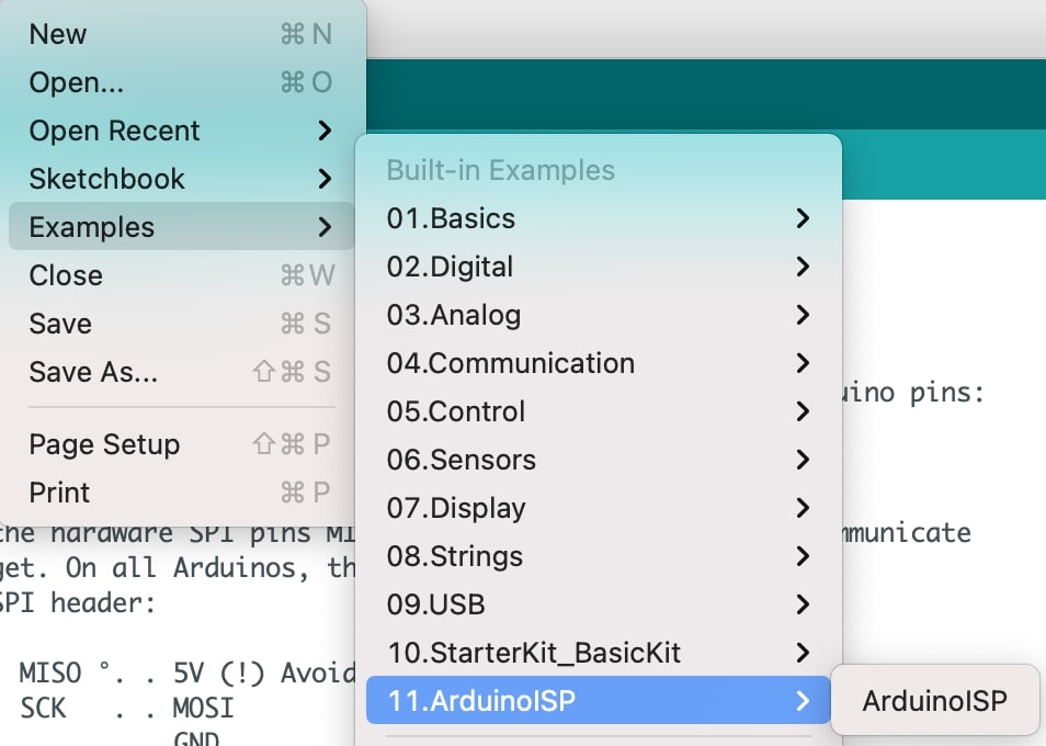
First I successfully uploaded the ArduinoISP sketch to the uno I had. I found this sketch under File->Examples->ArduinoISP.
After uploading the sketch I wired up the pins of the satshakit to the Arduino based on the diagram on the github page. This is how I had wired it up.
Arduino Satshakit Programmer Target 5V VCC GND GND 13 SCK 12 MISO 11 MOSI 10 RESET
However, whenever I tried to burn the Arduino bootloader onto the satshakit, I kept getting this error. I checked my wiring, my soldering, and even tried reuploading the ArduinoISP sketch onto the Arduino, but the same error persisted.
When trying to debug the issue, I then accidentally ripped the trace on the board that went to the VCC and GND header pins. Although this is mostly just a careless error, it didn’t help that I forgot to consider the width of the SMD headers when modifying the PCB design. Thus, I had to solder the VCC and GND headers as seperate since there wasn’t enough space to orient them sideways. Since each header was just a single pin, it made it very fragile and easy for the trace to rip, which unfortunately is exactly what happened.
With the trace being ripped, there was nothing else I could do but try and mill another board out and try reburning the bootloader.
Iteration 2: Modified Satshakit V2
This time, I didn’t want to make the same mistake as the previous time, and so I changed the PCB design and moved the button over to make space for the SMD headers. This would allow me to solder a two pin header on instead of two seperate 1 pin headers which are easy to break and aren’t stable. After making this change I went to remill using the exact same process as the previous time. Here are some images and videos of me milling the second time.
Here is an image of the 1/64 bit
Here is an image of the PCB 0.005 Engraving bit
Here is me locating the 1/64 bit.
Here is me probing the thickness with a 1/64th bit.
After milling out the board, I once again populated the board with the same components. It looked like this.
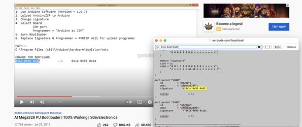
Having remilled and resoldered the components, next, I tried looking on the web for solutions to the error that I kept having with the first satshakit. At first, I found this forum post with someone who had gotten a similar error, but no resolution. On that forum, someone had suggested that I try and modify one of the avrdude.conf files, but there were no specifics as to how to do that. Eventually after some digging, I came across this video which seemed to explain the avrdude.conf file modifications. With no other ideas as to why I couldn’t burn the bootloader, I followed this video step by step.
This is the main instruction of the video, which is modifying this chip signature in the avrdude.conf file.
After trying this solution I still could not get the satshakit to work, interestingly with facing the exact same error as before. The error read
Yikes!  Invalid device signature.
Double check connections and try again, or use -F to override this check.
Finding no other solution whatsoever online to this problem, I turned again to Dr. Harris, who didn’t have a solution to the problem that I had not tried before. I was told that there could be many different causes to the problem which couldn’t be identified through my simple debugging. I was also told that people who have made satshakits at our lab in the past have experienced similar issues, but there have also been those who have gotten theirs working. There could be a problem with the Atmega chip model I was using, since there are many different kinds of Atmega328p chips, but it could also be a problem with the boards I had milled out. After a final check of the github page and online resources to make sure that there was anything that I hadn’t tried yet, I decided, for the sake of the week, to come back to the satshakit debugging at a later date.
Thus I began to work on a board that used an ATTiny1614 instead, going back to some more familiar ground. At some point in the future I definitely hope to return to the satshakit and get it working.
Iteration 3: ATTiny1614 Board
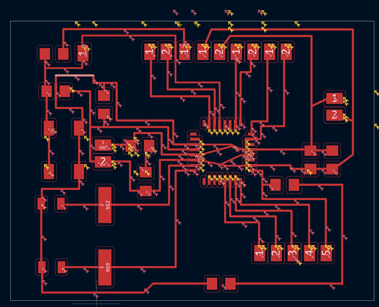
For this working iteration I designed a custom board from scratch using the same procedures I had used previously in KiCAD. If you want to see a full process of me designing a PCB in KiCAD, check out Week 07 Electronics Design. Here I simply put the schematic and PCB layout of the board.
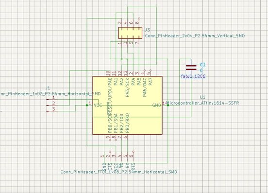
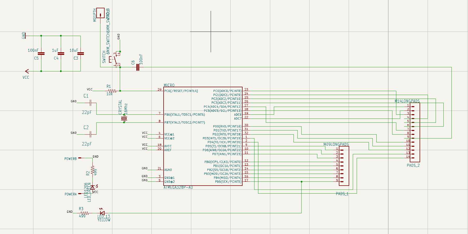
Here is the full schematic of the input boards, of which I made two of. Each board includes.
-
1x ATTiny1614
-
1x 6 pin FTDI header for serial communication
-
1x 3 pin UPDI header for UPDI programming
-
1x 2x4 header for the radio module (includes VCC, GND, CE, CSN, MISO, MOSI, SCK, and IRQ)
-
1x 1uF capacitor
-
1x 4 pin header for the joystick
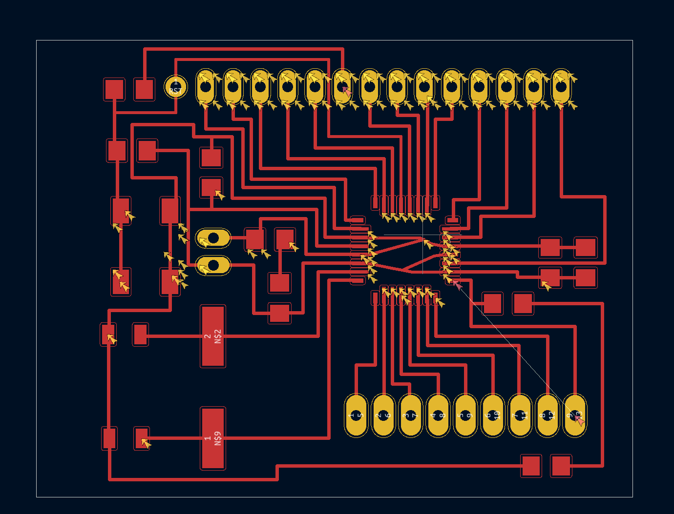
You can also notice that each board is capable of having the radio attached to it, so it serves multifunctions for networking and inputs. After finishing the schematic I brought it into PCB editor. Here is the PCB layout
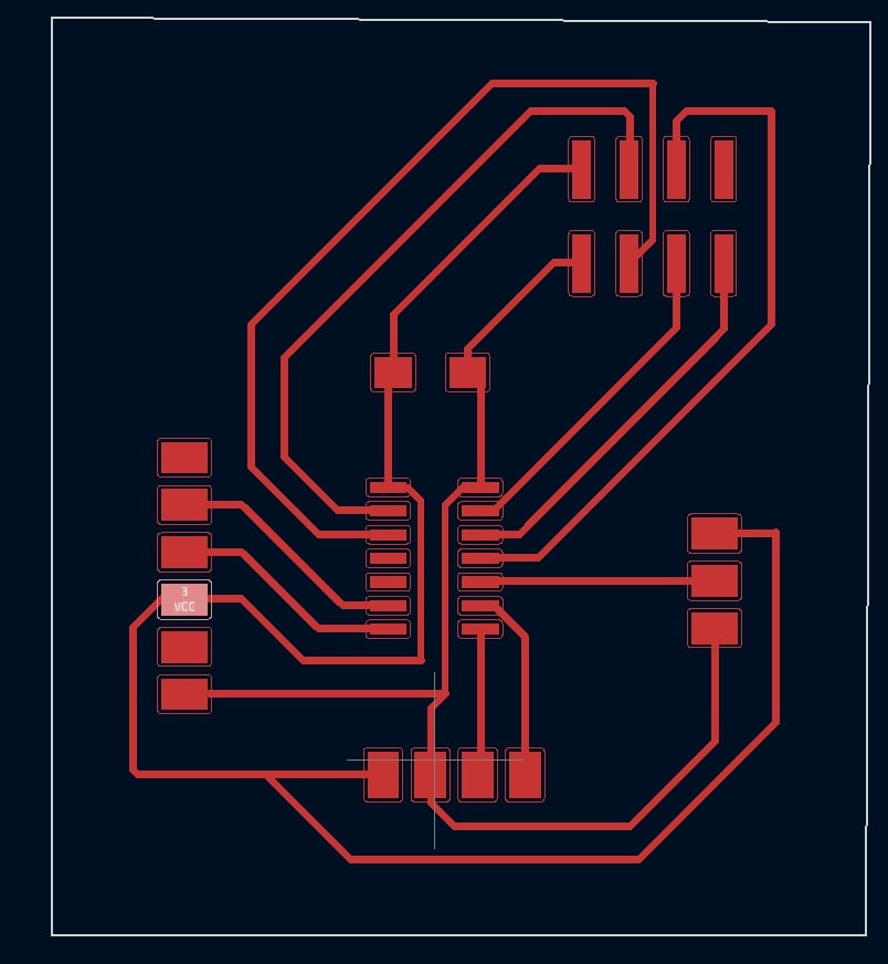
As you can see, some of the traces that go under a component are smaller to make shorts less likely to happen.
Next it was time for milling out the boards, which follows the same process as before.
Above is me probing the material
Above is the 1/64 milling
Above is the location of the 1/32 end mill
Above is the actual milling using 1/32 bit
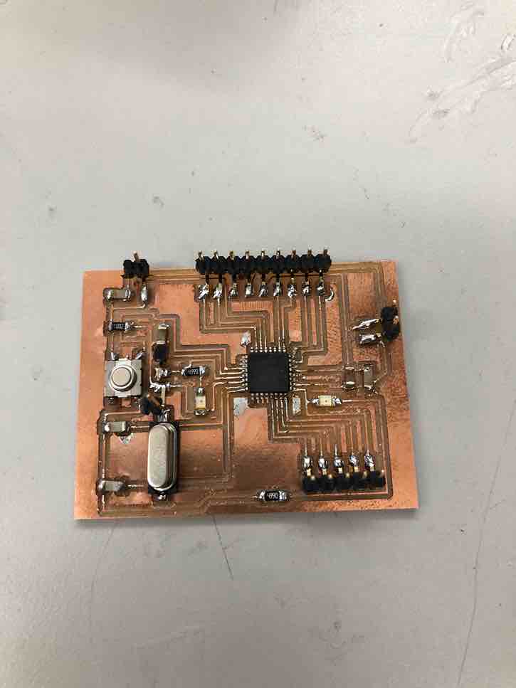
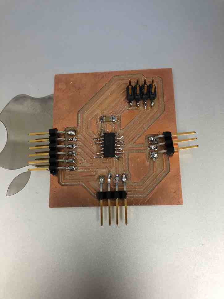
After all the milling, I populated the board with the same components I mentioned earlier. Here is how the finished hardware board looks.
Soldering and milling done, now it was time for the actual programming, which I took in very slow steps. First I made sure that the Arduino I was using actually functioned by uploading a simple blink sketch to it. This was successful.
Next I converted the Arduino into a jtag2updi programmer. I did this by uploading SpenceKonde’s jtag2updi.ino sketch found on the github repo to the Arduino.
Then I wanted to test basic serial capabilities of the new board I had just milled. I wrote some super basic serial code, then wired up GND, 5V, pin 6 of the Arduino to GND, VCC, UPDI of the Attiny. Here is the code
void setup() {
  Serial.begin(9600);
}

void loop() {
  Serial.println("hello");
  delay(100);
}
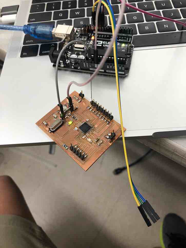
Here is me first uploading the sketch to the board.
Now I wired up the FTDI to USB connector to the Rx, Tx, VCC, and GND headers of the chip to read its serial output in the monitor.
Next it was time to wire up the joystick to the board, which I did. I followed my PCB layout diagram to assist me in wiring up the VCC, GND, Vrx, and Vry pins of the joystick, which were pins 7 and 6 of the attiny1614. Here is the code I used.
int VRx = 7;
int VRy = 6;

int xPosition = 0;
int yPosition = 0;
int mapX = 0;
int mapY = 0;

void setup() {
  Serial.begin(9600);

  pinMode(VRx, INPUT);
  pinMode(VRy, INPUT);

}

void loop() {
  xPosition = analogRead(VRx);
  yPosition = analogRead(VRy);
  mapX = map(xPosition, 0, 1023, -512, 512);
  mapY = map(yPosition, 0, 1023, -512, 512);

  Serial.print("X: ");
  Serial.print(mapX);
  Serial.print(" | Y: ");
  Serial.println(mapY);

  delay(100);

}
As you can see its practically the same as arduino joystick code except I replace pins A0 and A1 with 7 and 6. I am able to do this because both pins 7 and 6 can function as analog and digital pins depending on how you define them.
Here is the working final product.
Above is me uploading the code. This is me actually reading it out through the serial to FTDI cable I used prior.
Overall this was a big week for me, mainly because I started off with an idea that could have been used in my final project, and ultimately decided to put it off to a later date. I am still proud of what turned out, but now I am motivated as ever to get that satshakit working eventually. Joysticks are the main input for my quadcopter, so I’m still happy I was able to get some value recognized in the 1614 board. Plus, my 1614 boards have the dual purpose of networking and input capabilities, so most likely I will be using these boards for networking week too.
Week 13 Group Work
Jada, Pari, and I used Pari’s Doppler Radar Sensor because we are also testing analog inputs. Jada helped wire the radar and connected the Doppler Radar using the the ground power and analog pins. I helped set up the oscilloscope using this site they found while researching the sensor. Then Pari read the value off from the oscilloscope. They all took pictures, videos, and notes on how the oscilloscope functioned and how it connected to the sensor. The three figured out how to use the oscilloscope to help read whether the sensor was detecting movement or not. This is the result Pari recorded:
Click here to access the group site.
Week 13 Files
Click here to access my files for the week