13. Networking and Communications
This week we are working on communicating two devices through a networking protocol. The group assignment and individual assignment is as follows:
Group Assignment:
- Send a message between two projects
The link to the Group Assignment is available HERE
Individual Assignment:
- Design, build, and connect wired or wireless node(s) with network or bus addresses
Work Plan
| Days | Sessions | Time/Hour |
|---|---|---|
| Wednesday | Global Recitation | 7:00PM - 10:00PM BST |
| Thursday | Local Lecture and Research | 2 hours, 4 hours |
| Friday | Research / Board Design | 8hours/All Day |
| Saturday | Board Design and Soldering | All Day |
| Sunday | Testing with Two Boards | All Day |
| Monday | Working with BT Module / Documenting | All Day |
| Tuesday | Documenting | All Day |
Communication Protocols
Communication Protocols stands for a unified rules followed by two or more devices to exchange information or data between them. There are a number of communication protocols we learnt in our global and local lectures. The list of communication protocols and their examples are highlighted below:
Asynchronous Vs Synchronous Protocol
Two devices can communicate with each other in synchronous or asynchronous manner. The synchronous method of communication make use of a common clock signal for the two devices to comminicate with each other. When a clock signal is enabled then only is the data transmission initialted for a synchronous communication. An asynchronous communication happens between two devices without a common clock signal. Therefore a start and end bit needs to be sent for the data transmission to be successful.
The example of synchronous communication in real work can be a telephone or a video call where both parties are communicating at the same time for communication to be successful. An asynchronous communication on the other hand can be leaving messages and emails. The two parties donot have to be online for the communication to happen and can work in their own time.
Wired vs Wireless
Wired communication requires a hardware medium to connect two communicating devices. The two devices will make use of this medium to send and receive informations. The distance of the two communicating devices will determine the requirement of other intermediate devices such as amplifier, repeaters and routers. Wired comminication are more reliable due to the fact that they have less environment disturbances than wireless communication.
Wireless communication can occur between two devices through air as medium of communication path. These communication method has dependence on environmental factor and weather condition. Further, the range of communication depends on the type of communication protocol and standards in use. The communication protocols like WiFi and Bluetooth are short range and can work within a small area. GSM or mobile commnication has larger range while radio (FM and SW) have more distance coverage.
Different communication protocols are discussed below:
1. SPI(Serial Peripheral Interface) Protocol:
The SPI is a full duplex protocol which uses master slave configuration to establish communication. Motorola invented this protocol in 1980. SPI is used in microcontrollers with interfaces like EEPROM, LCD displays, etc.
SPI protocol comprises of four pins:
SCLK: Serial Clock ( Clock source for data transmission )
MOSI: Master Output Slave Input (Output data from Master)
MISO: Master Input Slave Output (Output data from Slave)
SS: Slave Select ( Slave selection from multiple slaves by Master)
Additional SS pins are necessary when master device needs to control more than one slaves. One master can control multiple slaves. SPI protocol supports high speed data transfer with bus speed typically stand around 50Mhz therefore the data transmission speed can go up to 50Mbps.
In our assignments, we have made use of the SPI protocol for a number of cases. The programming of the Attiny board using Fab ISP uses the same protocol. Through the same protocol, we also program our board using Arduino as ISP.
The master device has to select the slave to which the data needs to be sent using the Slave Select pin by activating a low input signal. Then the clock pulse from SCLK pin will be sent to slave to synchronize the transmission. The data from Master pin goes through MOSI pin and from slave to master comes through MISO pin.
2. I2C(Inter-Integrated Circuit) Protocol:
I2C is a two wire serial bus communication protocol invented in 1982 by Philips Semiconductors. It is a two-wire communication interface and commonly used to connect low-speed devices like microcontrollers, A/D and D/A converters, I/O devices and other peripherals in embedded systems.
I2C uses two pins to establish communication:
SDA: Serial Data Line
SCL: Serial Clock Line
I2C protocol supports different data speed based on their mode of operation. Data transfer speed 100kbit/s when operating in standard mode and 400 kbit/s when operating in full speed mode. The LCD makes use of I2C protocol to receive data from a microcontroller and display them. In I2C protocol each device is given a specific address. When a master wishes to transfer data to a slave, it sends the address of slave device through SDA pin for which the message is intended to. It is followed by Data frame and only the slave with the specified address will accept this incoming data.
3. USART(Universal Synchronous/Asynchronous Receiver/Transmitter) Protocol:
USART is a serial communication protocol developed by Digital Equipment Corporation in 1960’s. It supports Full duplex, Half duplex and simplex communication. This is one of the most popular protocol and will be in almost all microcontrollers
The communication in UART takes place through two pins.
RX: Receive the incoming data
TX: Transmits the outgoing data
Data transmission in USART takes place by means of data packets which usually consists of 8 data bits, start bits and parity bit to perform error correction. Data in USART will be sent in the form of data packets or data frame. The data frame starts with a start bit, followed by data bits and then by parity and stop bit. Most microcontrollers provide ways to configure the number of data bits and composition of the data frame. The serial communication between arduino and PC through USB make use of this protocol for communication through serial port.
4. CAN(Control Area Network) Protocol:
Controller Area Network or CAN protocol is designed to share data among multiple interfaces to reduce the complexity of connectivity and wiring. This was first developed and used in automobiles to establish communication between different parts of the automobile like engine, bakes, air conditioner etc while reducing the wiring in it. The unique feature about CAN protocol is that a data transmitted from one CAN device or node will be available to all the devices connected in the CAN bus.
This protocol uses two wires for communication with other CAN devices
- CAN HIGH
- CAN LOW
There are two types of CAN protocols: Standard CAN and Extended CAN.
In standard CAN any node can transmit data through the bus to any node. CAN data frame starts with a start bit followed by a 11 bit identifier which sets the priority of the message. Message with higher priority gains access to the CAN bus when two devices attempt to send message at the same time. RTR bit indicates if the data is being requested from a particular node. IDE bit marks whether it is a standard or extended CAN frame. Data length code bits follows IDE which indicates the length of data. Then comes the message itself. Cyclic redundancy check and ACK bits follows then and are used to error check to ensure proper transmission of data. A 7 bit end of frame which marks the end of the message.
5. USB(Universal Serial Bus) Protocol:
USB is one of the well developed and most used communication protocol. Despite having different standards and hardware types, it is considered to be versatile and effective in embedded systems. USB communication takes place by means of polling where the host device initiates the data transfer. When a device connects to the host it assigns address to the and uses it to perform data transfer.
USB protocol uses below pins to function
- VCC: For power supply
- GND: To close the circuit
- D+: Data transfer differential line
- D-: Data receive differential line
Every data transfer in a USB communication is done by means of data packets, Generally there are three components in a data packet : a token packet which carries information such as data type, device address. Next the datapacket which holds the actual data to be transferred and EOP to indicate the data packet is ended.
6. ETHERNET Protocol
Ethernet is most popular networking protocol used to establish connections right from LAN to WAN. With the growth in IOT, this protocol has become indispensable in Embedded systems. This communication protocol has undergone series of revisions over the years to enhance its connectivity and speed. Mostly Ethernet controller chips like WZ1500 will be used with regular microcontrollers to enable the Ethernet connectivity. However some high end Microcontrollers like STM32 will have some degree of inbuilt Ethernet protocol support within. Such microcontrollers use MII or RMII protocol to transmit and receive data within network
Transmission of data in Ethernet protocol takes the form of data frames. This data frame constitutes of senders address, receiver address, actual data and bits for error correction.
7. RS-485 Protocol:
RS-485 is yet another protocol popular for connecting microcontrollers with external peripherals. This protocol comes in very handy when the data need to be transmitted for over hundreds of meters. Similar to Ethernet protocol most microcontrollers uses external chips like MAX485 to use this protocol. Using this protocol several devices can use the same interface and perform data exchange. More about RS-485 protocol here. These are the pins involved in RS-485 protocol.
- TX+
- TX-
- RX+
- RX-
A typical data frame of RS-485 comprises of start bits, receiver address, data bits and stop bits to indicate the end of transmission.
Communicating between Two Boards
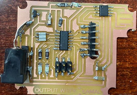
For the networking week, I am making use of two boards I made for the input and output week to communicate with each other. The input board contains a push button while the output board contains a motor driver. The details of the making of board is shown below:
Schematic Design
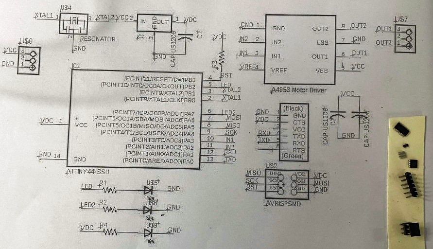
This week i will be working on communicating between the echo hello world board and the output board. In my final Project I will be making use of two motors as driving wheel for the Crawler Tank and this week will communicating between that board with a previously designed board.
Here I present the work done for the two weeks in designing the board for both the input and output week. I begin with the Schematic design in Eagle software which i have been using from the first session and have gotten used to. The basic starting and getting used to Eagle is in the Week6 - Electronics Design. I have documented details of working with Eagle where i made a hello world board and blinking of LED. The schematic of the two boards are shown in the figures below:
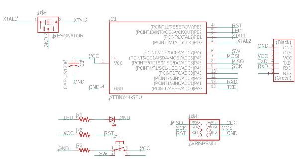
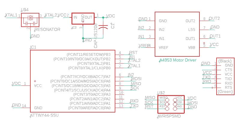
The motor driver i am using the the A4953. The 8 pin, H-Bridge driver is designed for pulse width modulated (PWM) control of DC motors, the A4952 and A4953 are capable of peak output currents to ±2 A and operating voltages to 40 V Datasheet of Driver. The peak current of the motor i am using is 1A and runs at 12V supply. It requires the voltage supply for the motor, a reference voltage of Vref. I am using Vref equal to Vcc after refering to Neil’s Driver circuit at Driver Circuit.
With the above connections made, I still have two pins free from the Attiny44 controller. Therefore I make use of them as signal pin to LEDs that signals the direction of the movement of the motor.

Since the motor runs at 12V while the controller runs at 5V, I am making use of a voltage regulator curcuit. The regulator provides a voltage of 5V at 100mA current. This should be enough to run the Attiny controller and few LEDs. While the external voltage supply of 12V will be supplied in parallel to the Motor Driver circuit.

Further, I make use of a power LED and capacitors closer to the motor diver side to protect from surges. The final schematic circuit is shown below.

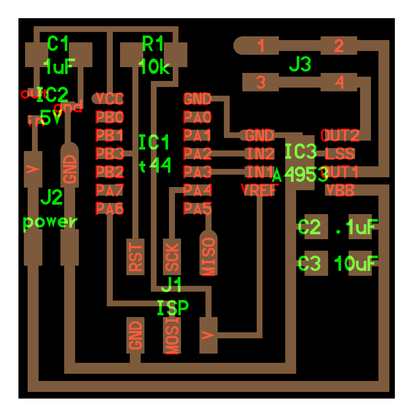
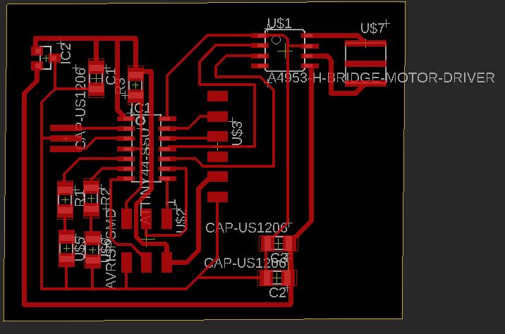
Board Design
With the schematic design completed, I move on to design of Board. I the board design, i drag all components to the board window and drag individual components to the desired location. The controller is centered, the power supply and regulator is kept on the left side while the driver is kept on the right. I referred to the Neil’s board for easy design.
In the routing, I am making use of larger trace width for Power and Vcc lines at 0.508mm while the signal traces are 0.3048mm. I do manual routing for the entire circuit with only two traces running through the controller while no traces run between the pins.
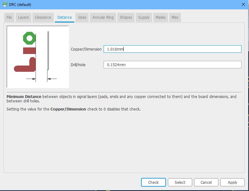
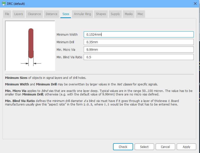
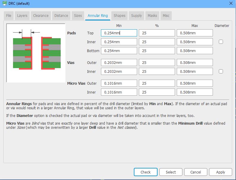
Then i perform DRC check for the design with the following settings.

![]()
The final board design of the two boards are shown below:

Milling the Board
The use of SRM20 milling machine is shown in Week 4- Electornic production week. With the board desing completed i take the png file for the trace and cut to mods and generate machine code (g-code) for SRM20 to mill. I make use of mods to generate the g-code. The details of that is also available in week4.

The milling and cut of the board is complete and i remove the the board for inspection. upon close inspection, i see that i have made a large trace width that passes between a component because of which the SRM20 left a small part without removing the traces. Since it was a small strectch, i remove the trace using knife and test for short using multimeter.

Soldering the components.
With the board milled, i move on to collecting the components and soldering them on the board.
I start the soldering with controller and driver first. The shorter and harder components are soldered first followed by resistors, LEDs and finally the connectors.


After soldering each components, I also use connectivity test to check if all solder connects the pins to the board. This way, it will eliminate the requiement of major debugging later. The soldered boards are shown below:

With the soldering of the components completed, I check to see if the power LED is working then I move on to programming and testing of the board.

Programming the boards
Initially, I begin with programming the two boards independently. After the two boards are programmed, they will be connected together and checked for connection between them. The logic of the communication is as follows:
- Since Attiny donot have serial, I have made use of software serial library and declared pin1 and Pin0 as Rx and Tx. For the two boards communicating, I swap and connect the Rx to Tx and Tx to Rx respectively.
- When a Button is pressed in Board I, It will send a signal to its Tx pin.
- Board II will read the signal at its Rx pin and based on the input of Rx pin , It will change the state of the LEDs.
- Then Board II also send a signal to Board I through its Tx pin which is read by Rx of Board I and changes the state of LEDs.
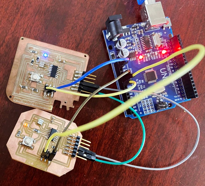
The two boards are connected individually to the Arduino board and programmed with arduino as ISP. The connection of the Arduino and board is shown below:

With the circuits connected to the arduino Board individually using SPI connection, I program the boards. The program code for the two boards is as follows:
#include <SoftwareSerial.h>
#define BUTTON 7
#define LEDPin 2
const int rx=1;
const int tx=0;
SoftwareSerial Serial(rx,tx);

void setup() {
  Serial.begin(9600);
  pinMode(BUTTON, INPUT);
}

void loop() {
    int ButtonMode = analogRead(BUTTON);
    Serial.print(ButtonMode);
    delay(100);
    if(Serial.available() > 0)
    {
    blinkLED();
    }
        }

void blinkLED()
{
digitalWrite(LEDPin, HIGH);
delay(200);
digitalWrite(LEDPin, LOW);
delay(200);
digitalWrite(LEDPin, HIGH);
delay(200);
digitalWrite(LEDPin, LOW);
delay(200);
digitalWrite(LEDPin, HIGH);
delay(200);
digitalWrite(LEDPin, LOW);
delay(200);
}
//ATtiny Pin5,6 - LED Arduino (8,7)
//Attiny Pin 10,11 - in1,in2 Arduino (3,2)
#include <SoftwareSerial.h>
#define BUTTON 7
#define LED 8
const int rx=0;
const int tx=1;
SoftwareSerial Serial(rx,tx);

void setup()
{
Serial.begin(9600);
pinMode(LED, OUTPUT);
}

void loop() {
int ButtonMode = digitalRead(BUTTON);
if(Serial.available() > 0)
{
blinkLED();
Serial.print(ButtonMode);
delay(200);
}
}

void blinkLED()
{
digitalWrite(LEDPin, HIGH);
delay(200);
digitalWrite(LEDPin, LOW);
delay(200);
digitalWrite(LEDPin, HIGH);
delay(200);
digitalWrite(LEDPin, LOW);
delay(200);
digitalWrite(LEDPin, HIGH);
delay(200);
digitalWrite(LEDPin, LOW);
delay(200);
}
With the program code uploaded to individual boards, i move on to make the connection of the two boards using the Rx and Tx pins. I power the two boards using Vcc and GND pins from the arduino board. The curcuit of the same is shown below:
The video below shows the working of the circuit when the button is pressed.
I2C Communication between two boards
I2C stands for the inter-integrated controller. This is a serial communication protocol that can connect low-speed devices. It is a master-slave communication in which we can connect and control multiple slaves from a single master. In this, each slave device has a specific address (source: tutorialpoint).
Unlike SPI comminucation, I2C communication donot have a slave select pin. The I2C communication consist of only two pins that are:
- SDA (Serial Data) – The channel used by the master and slave to send and receive data.
- SCL (Serial Clock) – Common clock signal.
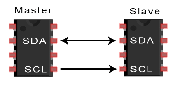
I2C is a serial communication protocol, so data is transferred bit by bit along a single wire (the SDA line). Like SPI, I2C is synchronous, so the output of bits is synchronized to the sampling of bits by a clock signal (SCL line) shared between the master and the slave. The clock signal is always controlled by the master (1). I2C bus need two pull-up resistor 4.7 kohm, one at the SDA line and one at the SCL line. If the resistor is missing, the SCL and SDA lines will always be low and the I2C bus will not work. Source:https://www.circuitbasics.com/
Working of I2C Communication With I2C, data is transferred in messages. Messages are broken up into frames of data. Each message has an address frame that contains the binary address of the slave, and one or more data frames that contain the data being transmitted. The message also includes start and stop conditions, read/write bits, and ACK/NACK bits between each data frame:
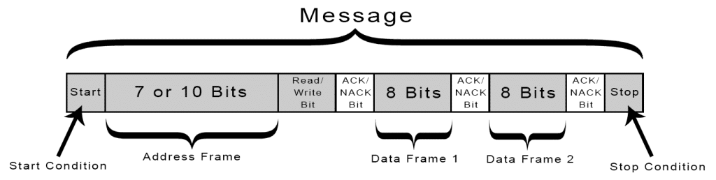
Start Condition: The SDA line switches from a high voltage level to a low voltage level before the SCL line switches from high to low.
Stop Condition: The SDA line switches from a low voltage level to a high voltage level after the SCL line switches from low to high.
Address Frame: A 7 or 10 bit sequence unique to each slave that identifies the slave when the master wants to talk to it.
Read/Write Bit: A single bit specifying whether the master is sending data to the slave (low voltage level) or requesting data from it (high voltage level)
ACK/NACK Bit: Each frame in a message is followed by an acknowledge/no-acknowledge bit. If an address frame or data frame was successfully received, an ACK bit is returned to the sender from the receiving device.
Addressing
I2C doesn’t have slave select lines like SPI, so it needs another way to let the slave know that data is being sent to it, and not another slave. It does this by addressing. The address frame is always the first frame after the start bit in a new message.
The master sends the address of the slave it wants to communicate with to every slave connected to it. Each slave then compares the address sent from the master to its own address. If the address matches, it sends a low voltage ACK bit back to the master. If the address doesn’t match, the slave does nothing and the SDA line remains high.
I2C between Arduino and Two Attiny Boards
In this assignment, i want to connect two Attiny boards in I2C communication protocol with an Arduino Board as Master.
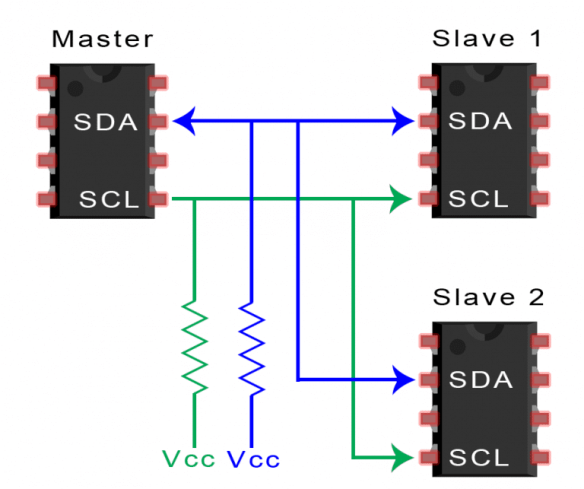
Circuit Connection
The circuit for the I2C communication between Arduino as Master and Two Attiny boards as slave is shown below:
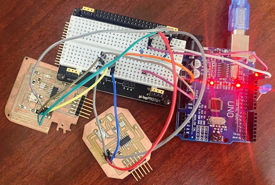
For the individual Attiny boards, I first upload the codes using Arduino as ISP through the ISP programming Pins. The Attiny has common pins for programming and communication. The SDA pin in Attiny is also the MOSI pin and the SCK pin is the SCL pin. After programmin the Attiny slave devices individually, I move on to program the Arduino board with the program for Master. As we can see in the codes below, the address for the boards are defined and declared in both the Attiny boards individually and in the master device.
I make use of the code below to program the boards.
Codes
//Arduino as Master, Takes input from Serial port and performs task as per the case
//Case 0 - blinks Arduino LED, Case 1 - Send for Hello Board Blink, Case 2 - Send for Output board Blink and motor

#include <Wire.h>
#define slave1 (1)
#define slave2 (2)

const int ledPin =10;
int times = 3;

void setup(){
  Wire.begin();
  Serial.begin(9600);
  Serial.println("Serial Communication Ready,Enter '0' for Master, '1' for Slave 1, '2' for Slave '2'");
  pinMode(ledPin, OUTPUT);
}

void processCmdChar(char cmd) {
  switch (cmd)
  {
    case '0':
      blink_LED(times);
      break;
    case '1':
      Wire.beginTransmission(slave1);
      Wire.write(times);
      Wire.endTransmission();
      break;
    case '2':
      Wire.beginTransmission(slave2);
      Wire.write(times);
      Wire.endTransmission();
      break;
  }
}

void blink_LED(int times){
  while (times--)
  {
    digitalWrite(ledPin, HIGH);
    delay(200);
    digitalWrite(ledPin, LOW);
    delay(200);
  }
}

void loop(){
  if(Serial.available())
  {
    char cmd = Serial.read();
    Serial.print("Command from cmd was: ");
    Serial.println(cmd);
    processCmdChar(cmd);
  }
  delay(500);
}
//Slave 1 : Attiny 44 Hello World Board
//Reads value using TinyWire and performs Blinkfunction if it is selected.
// Since Attiny donot have Wire.h, similar function called TinyWireS is used instead

#include <TinyWireS.h>
#define I2C_SLAVE_ADDRESS (1)
const int ledPin = 3;
byte received = 0;

void setup()
{
  TinyWireS.begin(I2C_SLAVE_ADDRESS);
}

void blink_LED(int times){
  while(times--){
    digitalWrite(ledPin, HIGH);
    delay(200);
    digitalWrite(ledPin, LOW);
    delay(100);
  }
}

void loop(){
  if (TinyWireS.available()){
    received = TinyWireS.read();
    blink_LED(received);
  }
  received = 0;
  TinyWireS_stop_check();
}
//Slave 2 : Attiny Hello World Board
//Reads value using TinyWire and performs Blinkfunction if it is selected.
// Since Attiny donot have Wire.h, similar function called TinyWireS is used instead

#include <TinyWireS.h>
#define I2C_SLAVE_ADDRESS (2)
#define LED1 8
byte received = 0;

void setup()
{
  TinyWireS.begin(I2C_SLAVE_ADDRESS);
}

void blink_LED(int times){
  while(times--){
    digitalWrite(ledPin, HIGH);
    delay(200);
    digitalWrite(ledPin, LOW);
    delay(100);
  }
}

void loop(){
  if (TinyWireS.available()){
    received = TinyWireS.read();
    blink_LED(received);
  }
  received = 0;
  TinyWireS_stop_check();
}
The Arduino as master device choose the board to communicate with from the Serial monitor as user input. And based on the input, it performs the required communication.
When a ‘0’ is read from the serial monitor, the LED connected to the Arduino blinks
Initial State
When 0 is read from Serial Monitor
When a ‘1’ is read from the serial monitor, the Arduino sends communication signal to Attiny through the I2C channel. The Attiny compares the address and the first slave device is selected. That enables the Attiny1 to blink the LED.
When 1 is read from Serial Monitor
When a ‘2’ is read from the serial monitor, the Arduino sends communication signal to Attiny through the I2C channel. The Attiny compares the address and the Second slave device is selected. That enables the Attiny2 to blink the LED three times.
Learning and Outcomes
- Through the task this week, I have learnt to create communication between two attiny using software serail communication since serial communication donot work directly in Attiny.
- I have also learnt to communicate between one master and two slave device through I2C communication protocol. The I2C is simplier as it uses only two pins and the slave select is defined in the communication payload.
Reference
Communication Protocol Reference Circuit Basics for I2C Protocol
Program Code
Program Codes Week 13 Program Codes Serial Program Codes I2C