6. Electronics Design

This week I worked on design of electronic circuits and its board design. We also used software to simulate the operation of the circuit.
Assignment
Group Assignment:
- Use the test equipment in your lab to observe the operation of a microcontroller circuit board.
Link to the Group Assignment is available HERE
Individual Assignment:
- Redraw an echo hello-world board,
- Add (at least) a button and LED (with current-limiting resistor)
- Check the design rules, make it, and test that it can communicate
- Extra credit: simulate its operation
Starting Point
I begin the week with testing of a couple of softwares. I am familiar with PSpice too for similation of circuits and I also made use of Eagle software to draw the circuit and its board. Further I did test of the design rules and programmed the board so that we can see that it works with both the inputs and outputs.
Starting with Eagle Software.
We first start the eagle program. Since the license we are using is student version, we also login to the system before we start using it.
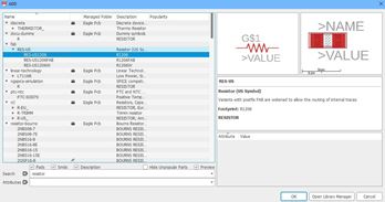
Once in the program, we create a new project and in the project we create a new schematic to make the schematic circuit. Once in the schematic window we add parts from the library.
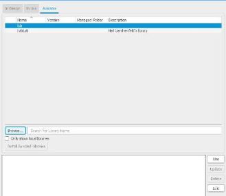
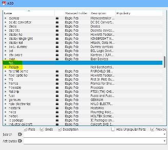
There are various library that we can use to make the circuit. In the fabacademy we are making use of SMD components and the libraries are available online. We download the library from the online protal https://github.com/Academany/FabAcademany-Resources and then add it to the Eagle libraries.
Adding Library and Drawing Circuit
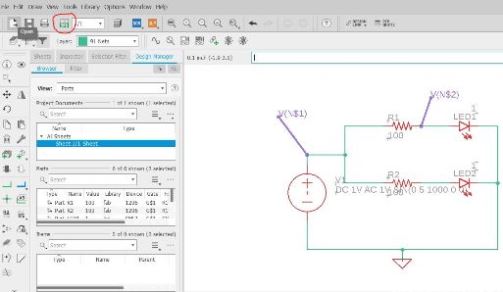
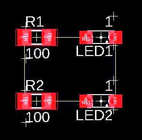
Once the libraries are added to the software, we can make use of it to create a circuit. For the first trial, I made a simple circuit with two resistors and two LEDs. This circuit donot have any specific use but was used as tutorial for learning purpose. The circuit is build by dragging the components from the library and then creating wires using NET

There are a couple of shortcut keys that can be used to get to different places in Eagle, but i am not famalier with most to use them consistently. However, we can type the part name on the search bar to navigate faster. After drawing the first circuit, I tried a basic software simulation to see if the circuit works. Here i have used a sine wave to test the input and the output side of the circuit. A ground is also connected to get a return path for the circuit. Further i make use of two voltage probes to measure and visuallize the voltage.
Circuit Simulation Setup

The Eagle software prompts for us to MAP the components to an equivalent Spice model. Once the mapping is successful we can simulate it. Prior to simulation, we have to provide values to source and components. Further, we change the simulation setting and provide values appropriately. First I did a transient response to plot the input and output waveform. There are other simulations that we can perform in Eagle namely:
- Operating Point
- DC Sweep
- AC Sweep
- Transient
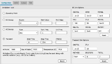
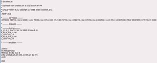
With the transient simulation setup, I run the simulation to look at the input and output. The software also generates the netlist that we can check to look at the circuit equivalent.
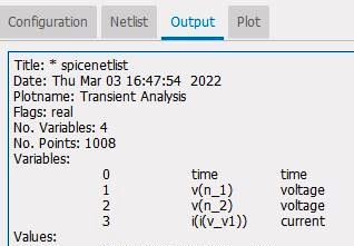
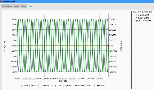
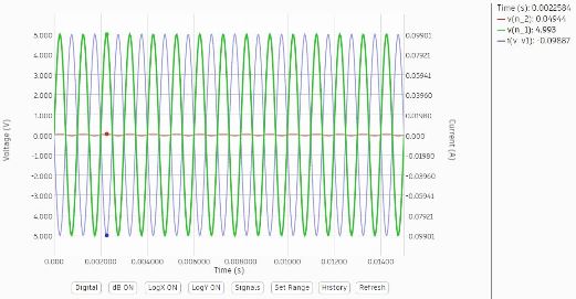
Circuit Simulation Result
The simulation result is shown in the figure below. Since we are looking at the output after a resistor, we will see that the voltage is zero as we have a 0Ohm LED. In ideal case that would be true, However if we have a small impedance of the LED, then we will see that the voltage at Node-2 is voltage across the LED. The value compared to the input will have no change in other parameters namely the frequency and phase.
Circuit to Board
After the circuit simulation i convert the cicuit to PCB equivalent. This can be achieved from: File > Switch to Board. This transforms the schematic to board equivalent using components. The components/models are open in a board page.
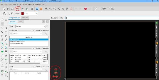
Now the components are dragged and dropped into the window and we make manual arrangement so that they are placed appropriately. One of the best method I used is to compare the board with the schematic and make the component placements resemble schematic. However, best component placement will ensure least trouble in connecting them. The connections are also imported along with the components from schematic and needs to be aligned.
Once the components are placed in the board, we can manually align and placed such that the traces donot intersect. Care should be taken such that the design rules are not missed and the board design donot throw any errors.
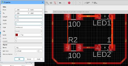
Routing on Board
Once the components are placed, we can make use of either auto routing or route manually.
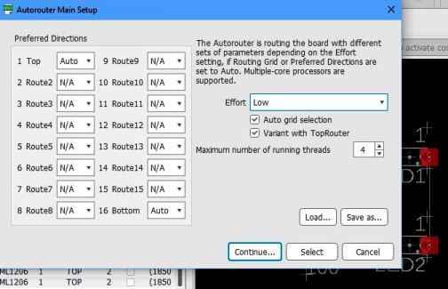
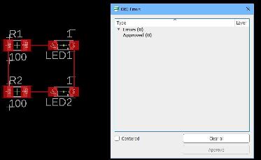
For simplier circuits, autorouting donot create many errors from design rule however, complex circuits would throw design errors when using autoroute. Further, the number of traces passing under a component should also be limited to two while no trace would pass between pins of a controller to ensure that we donot have problem in soldering or shortcircuit. Once the routing is completed we can look at the errors if any using DRC (Design Rule Check). If any design rules have been broken, it will throw an error.
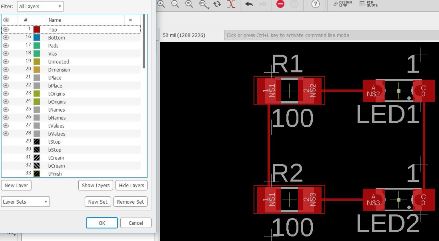
With no errors in design rule, we proceed to layers and keep only the layers of interest so that the milling donot create mess of the design. The top-layer is retained while all other layers are removed.
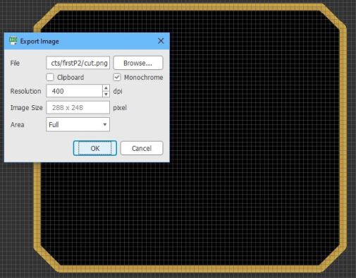
Exporting Board to PNG
The size of the traces are also properly set. We can do this at the time of routing so that we donot have to manually change later.
Now with the board design complete, we can export the trace and cut using export command. We can also use the dimension command to look at the size of the board.

Echo Hello-World Board
For the individual assignment we are supposed to draw a hello world board on schematic and create its board. I am making use of Eagle software to accomplish this. In the previous section I have done a detail of the method used to create the board from schematic and exporting to png. For the hello world board as well, I begin with the schematic. Since the number of components is more and connections complex i have used labels instead of making all connections to pins. This will help better visuallize the circuit and reduce errors.
Using a circuit as a reference, I made a schematic of the circuit on eagle software. From the circuit, we can see that there is:
- One controller (Attiny44)
- Two Resistors
- One LED
- One Push Button
-
One AVRISP Header Connector
-
One FTDI Connector (USB to Serial (TTL level) converter).
Using the fab eagle libraries, I constructed the circuit as shown below.
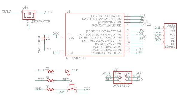
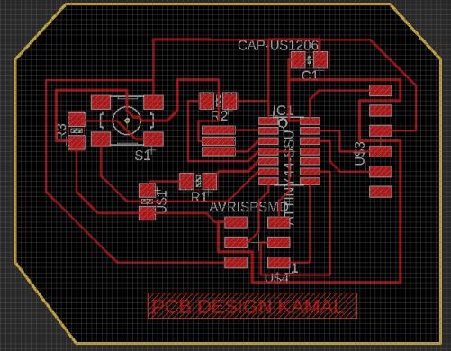
The schematic contains the basic requirement of controller, LED and Resistor and header for programming and communication. After the design of the schematic is complete, I move to design of the board. The process is similar to what i have used in the tutorial above. The components from schematics are exported to board design window. I drag and drop the components to the design window within a board trace.

With the components placed in the workspace, I begin by placing the components based on the schematic and best fit possible. Then I ran an auto route for the routing to look at the best routing the system can perform. It turns out that there are couple of errors that is generated. Further, a number of routes run between the pins of the controller which is not desirable given the spacing of the controller pin. Therefore, I moved on to manual routing.
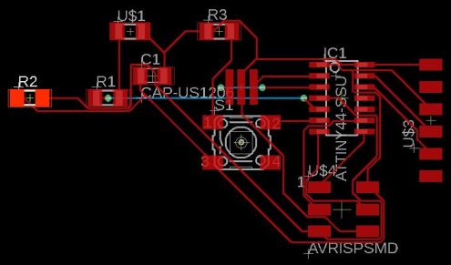
I make the primary routes of the Vcc and Gnd since these lines run the most and covers the maximum of the components. Then i looked at the common points and components and made remaining routes.

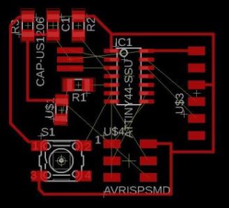
The final few routes are the more difficult to connect but with proper analysis and survey I was able to make all the routes successfully.

Few Design Rules
- No routes run between the controller pins
- The minimum trace width is 10mil or 0.254mm.
- Maximim of two traces run under the controller or any other component.
Design Rule Settings
The figure below shows the design rule for the design before making the traces and running the DRC. I have made use of a minimum of 0.254mm wire width and spacing.
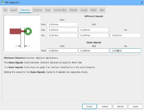
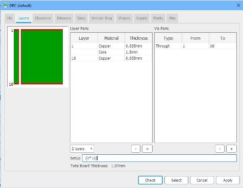
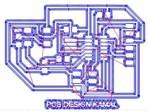
Using the above design rules, I complete the Design Rule Check (DRC) successfully before exporting the two files (trace and cut) as PNG.
Then we change the layers and create the cut and trace .PNG files by exporting as image. These files will be used to produce PCB.
Printing the Echo Hello-World Board
We follow the method from the week 4 Electronic Production to print the board on SRM20 PCB milling machine. Summary of steps used are.
-
Used MODs to create machine readable rml file
-
Load the RML file to V-Panel for SRM20

-
Print the PCB using SRM20
- Cut the PCB using SRM20
-Final PCB Cut

Soldering the Echo Hello-World Board
Once the PCB is milled, we move to Soldering. We follow the process as in week 4 Electronic Production to solder the components to the board.
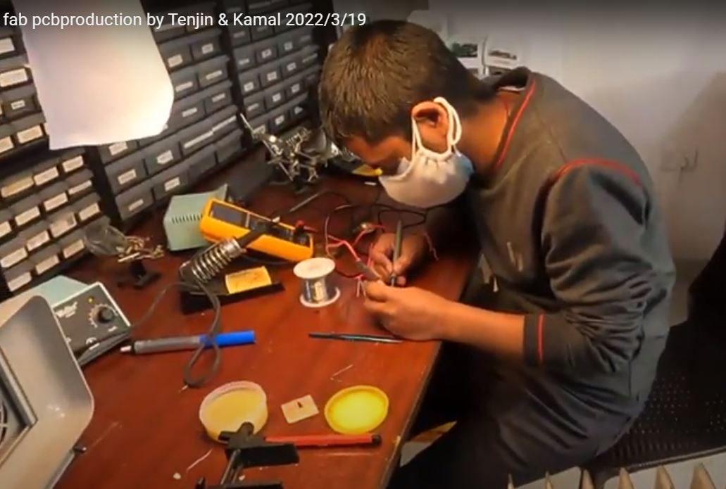
I begin by collecting the components first then soldering one component at a time. The time required for me to complete the soldering was more than an hour.

Programming the Echo Hello-World Board
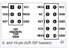
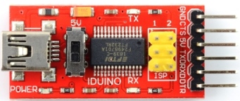
After completing the soldering of the components on board, We proceed to programming the board. Initially we started by programming the board using Arduino as programmer. To Program the board using arduino as programmer, we first look at the pins connection between Attiny44 and Arduino board.
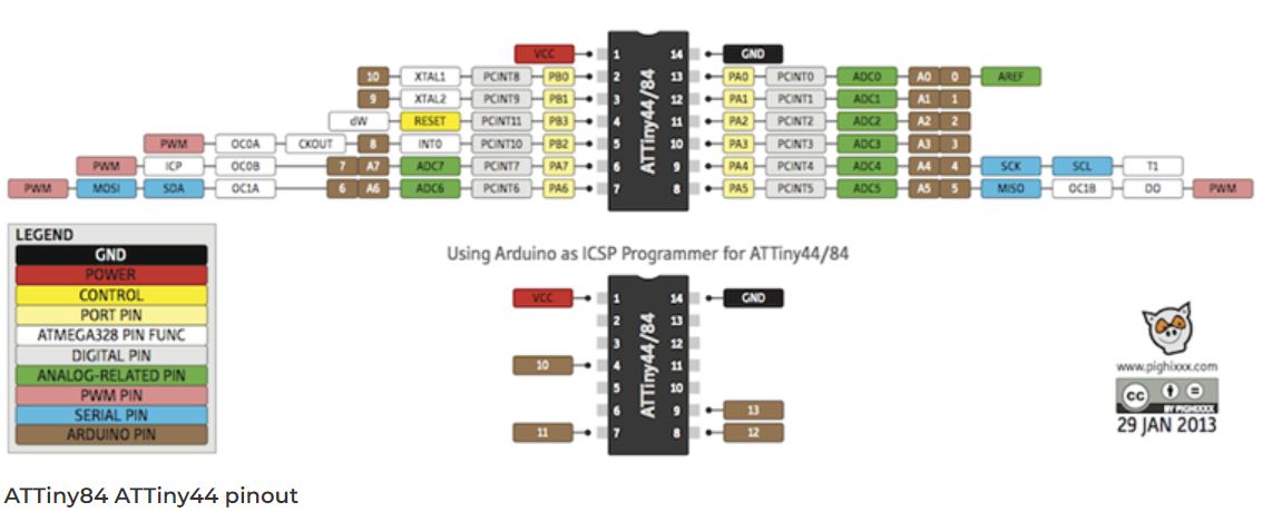
With the help of the pin diagram above, we make the connection to the arduino board and the hello world board. The arduino is initially used as a programmer to program the attiny hello world board.

We also choose the board to program. The board is initially not available on Arduino IDE. Therefore we have to download it from the internet and add it to the library of the IDE. In the Arduino IDE, we go to preference and add additional board manager URL. The file for the additional board manager is available on Github

With the json file added to the preference, the board will now be available on the board managers of arduino IDE.

With the board now available for programming and connections completed as required, we change the settings on the IDE as below:

Then we can use a simple blink LED program to check whether we can program the board or not. If the bootloader runs successfully without errors we can tell that the programming was successful, then we can check the functionality of the board. We can also add an input pin for the button such that, when the button is pressed, the LED will glow or any other function similar to that.
The blinking of the LED is shown in the video above.
Code Example of Blinking LED
// the setup function runs once when you press reset or power the board
void setup() {
  // initialize digital pin LED_BUILTIN as an output.
  pinMode(2, OUTPUT);
}

// the loop function runs over and over again forever
void loop() {
  digitalWrite(2, HIGH);   // turn the LED on (HIGH is the voltage level)
  delay(1000);                       // wait for a second
  digitalWrite(2, LOW);    // turn the LED off by making the voltage LOW
  delay(1000);                       // wait for a second
    digitalWrite(2, HIGH);   // turn the LED on (HIGH is the voltage level)
  delay(1000);                       // wait for a second
  digitalWrite(2, LOW);    // turn the LED off by making the voltage LOW
  delay(1000);
}
Circuit Function Simulation using Proteus
Proteus Design Suite electronic design automation
The Proteus is a proprietary software that works well in simulating the functionality of electronic systems that contain controller blocks. The GUI is also user friendly compared to other simulation tools where the visualization consists of waveforms. For design and simulation of system with proteus, the process remains exactly same as all other softwares including
- Creating Project.
- Libraries and Components.
- Drag/Drop or select components from list to schematic window.
- Make wire connections.
Further, we can generate .hex file of the program code we use for hello world board and use it to virtually program the controller in proteus. It just requires us to compile program on arduino IDE. Arduino IDE generates .hex file along with other output files. We load the hex file into the controller by browsing to the file location from the software. We can then simulate the operation of the system and visuallize the outcomes. The operation of the LED blinking process is shown in the video below.
Project Files
- Test PNG File Trace: Test PNG File Trace.png
- Test PNG File Cut: Test PNG File Cut.png
- Tutorial Eagle Project Files: Tutorial Project Files.rar
- Hello World Eagle Project Files: Hello World Project.rar
- RML file for Hello World Board: RML file for Hello World
- Proteus Design File: Proteus Simulation Design File