8. Embedded Programming
This week I worked on Embedded programming both individually and in group.
Individual Assignment
- Read the data sheet for your microcontroller
- Use your programmer to program your board to do something
- Extra credit: try other programming languages and development environments
Group Assignment
- Compare the performance and development workflows for other architectures
- The link to the Group Assignment for the Embedded Programming week is in Group Week 8
Reading Data Sheet of Microcontroller
Attiny 44 Datasheet
For the current assignment, I am making use of Attiny44 microcontroller for blinking of LED. From the Attiny microcontroller i make use of the datasheet from the following website: Attiny Controller Datasheet
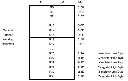
The attiny controller uses a RISC (Reduced Instruction) instruction set with 120 instructions where each instruction run with single clock cycle. This improves the speed of operation compared to CISC with 32 x 8 registers. I have taken the following basic specifications from the datasheet.

Figure: Attiny44 AVR Architecture Diagram taken from Datasheet.
Non-volatile program and data memories
- 2/4/8K byte of in-system programmable program memory flash (Atmel® ATtiny24/44/84)
- Endurance: 10,000 write/erase cycles
- 128/256/512 bytes in-system programmable EEPROM (Atmel ATtiny24/44/84)
- Endurance: 100,000 write/erase cycles
- 128/256/512 bytes internal SRAM (Atmel ATtiny24/44/84)
- Programming lock for self-programming flash program and EEPROM data security
Peripheral features
- Two Timer/Counters, 8- and 16-bit counters with two PWM channels on both
- 10-bit ADC
- Eight single-ended channels
- 12 differential ADC channel pairs with programmable gain (1x, 20x)
- Temperature measurement
- Programmable watchdog timer with separate on-chip oscillator
- On-chip analog comparator
- Universal serial interface

Figure: Attiny44 Block Diagram taken from Datasheet.
Special microcontroller features
- debugWIRE on-chip debug system
- In-system programmable via SPI port
- External and internal interrupt sources
- Pin change interrupt on 12 pins
- Low power idle, ADC noise reduction, standby and power-down modes
- Enhanced power-on reset circuit
- Programmable brown-out detection circuit
- Internal calibrated oscillator
- On-chip temperature sensor
- Automotive temperature range
- Low power consumption
I/O and packages
- 14-pin SOIC, 20-pin QFN/MLF: Twelve programmable I/O lines
Looking at the specification, the number of I/O lines are sufficient for a number of low end applications requiring less computations owing to its 32 x 8 registers to process. Further the Attiny controller also has very less programmable memory of
Attiny44 Pin Diagram

Operating voltages and Speed
Operating voltage:
- 2.7 - 5.5V for Atmel ATtiny24/44/84
The operating voltage is suitable to be used with any 5 volt supply with the range of milliAmperes currents. However, for output devices requiring higher current ratings will need the use of additional external voltage supply that can supply the required current. For my case of output device that I will use in my final project, I will have to make use of external power supply with higher current handling capacity.
Speed grade
- Atmel ATtiny24/44/84: 0 - 8MHz at 2.7 - 5.5V, 0 - 16MHz at 4.5 - 5.5V
- Active mode:
- 1MHz, 2.7V: 800µA
- Power-down mode:
- 2.7V: 2.0µA
ESP32 Datasheet
The ESP32 is a ESP32 is a single 2.4 GHz Wi-Fi-and-Bluetooth combo chip designed with the TSMC ultra-low-power 40 nm technology. It is designed to achieve the best power and RF performance, showing robustness, versatility and reliability in a wide variety of applications and power scenarios (source:Datasheet).

Figure: ESP32 Pin Diagram.
CPU and Memory
- Xtensa® single-/dual-core 32-bit LX6 microprocessor(s)
CoreMark® score:
– 1 core at 240 MHz: 504.85 CoreMark; 2.10 CoreMark/MHz
– 2 cores at 240 MHz: 994.26 CoreMark; 4.14 CoreMark/MHz - 448 KB ROM
- 520 KB SRAM
- 16 KB SRAM in RTC
- QSPI supports multiple flash/SRAM chips
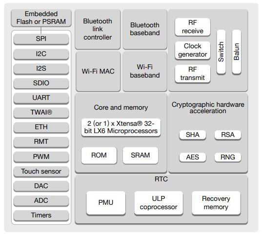
Figure: ESP32 Block Diagram.
Clocks and Timers
- Internal 8 MHz oscillator with calibration
- Internal RC oscillator with calibration
- External 2 MHz ~ 60 MHz crystal oscillator (40 MHz only for Wi-Fi/Bluetooth functionality)
- External 32 kHz crystal oscillator for RTC with calibration
- Two timer groups, including 2 × 64-bit timers and 1 × main watchdog in each group
- One RTC timer
- RTC watchdog
Advanced Peripheral Interfaces
- 34 × programmable GPIOs
- 12-bit SAR ADC up to 18 channels
- 2 × 8-bit DAC
- 10 × touch sensors
- 4 × SPI
- 2 × I2S
- 2 × I2C
- 3 × UART
- 1 host (SD/eMMC/SDIO)
- 1 slave (SDIO/SPI)
- Ethernet MAC interface with dedicated DMA and IEEE 1588 support
- TWAI®, compatible with ISO 11898-1 (CAN Specification 2.0)
- RMT (TX/RX)
- Motor PWM
- LED PWM up to 16 channels
- Hall sensor
ESP32 Power Scheme
ESP32’s digital pins are divided into three different power domains:
- VDD3P3_RTC
- VDD3P3_CPU
- VDD_SDIO
VDD3P3_RTC is also the input power supply for RTC and CPU.
VDD3P3_CPU is also the input power supply for CPU.
VDD_SDIO connects to the output of an internal LDO whose input is VDD3P3_RTC.
When VDD_SDIO is connected to the same PCB net together with VDD3P3_RTC, the internal LDO is disabled automatically. The power scheme diagram is shown below:

For the use of ESP32 Board, the power supply is of utmost importance because the ESP makes use of 3.3V while most of the other system work with 5V power supply. Since 5V power supply are mostly universal, we have to use a voltage regulator circuit additional for the system so that a proper power supply is available for the ESP. Further, when most of the peripherials makes use of 5V, two power supplies maybe required. Additionally, for I/O devices requiring higher current, external power supply is also required.
Radio Scheme
The radio module for ESP32 consists of the following blocks:
- 2.4 GHz receiver
- 2.4 GHz transmitter
- Bias and regulators
- Balun and transmit-receive switch
- Clock generator
The radio scheme for the ESP32 is use for wireless communication using WiFi or Bluetooth technology.
WiFi MAC
The ESP32 Wi-Fi MAC applies low-level protocol functions automatically. They are as follows:
- 4 × virtual Wi-Fi interfaces
- Simultaneous Infrastructure BSS Station mode/SoftAP mode/Promiscuous mode
- RTS protection, CTS protection, Immediate Block ACK
- Defragmentation
- TX/RX A-MPDU, RX A-MSDU
- TXOP
- WMM
- CCMP (CBC-MAC, counter mode), TKIP (MIC, RC4), WAPI (SMS4), WEP (RC4) and CRC
- Automatic beacon monitoring (hardware TSF)
Bluetooth Radio and Baseband
The Bluetooth Radio and Baseband support the following features:
- Class-1, class-2 and class-3 transmit output powers, and a dynamic control range of up to 21 dB
- π/4 DQPSK and 8 DPSK modulation
- High performance in NZIF receiver sensitivity with a minimum sensitivity of -94 dBm
- Class-1 operation without external PA
- Internal SRAM allows full-speed data-transfer, mixed voice and data, and full piconet operation
- Logic for forward error correction, header error control, access code correlation, CRC, demodulation, encryption bit stream generation, whitening and transmit pulse shaping
- ACL, SCO, eSCO, and AFH
- A-law, µ-law, and CVSD digital audio CODEC in PCM interface
- SBC audio CODEC
- Power management for low-power applications
- SMP with 128-bit AES
For the current assignment, I have studied two datasheet namely the ESP32 and Attiny44 datasheet. In the class assignments, I am making use of the Attiny44 controller to study input and output devices mainly due to its availability and ease of designing them and soldering them. However, for the Final project, I need to make use of the ESP32 camera module, and hence I will be using ESP32 controller board connected to a OVR camera and peripherials.
While a large chunk of GPIO pins will be used by the camera module, I can still make use of a couple of the unused pins to communicate with other input and output devices.
Programming of Board
In Week6:Electronics Design we completed the design of a Hello world board that has an input push button and an output LED.

Using the Hello world board and the programmer that we fabricated in Week4 Electronics Production we would program the hello world board to blink the LED.

The process of programming the board is as follows:
Programming the Board with Arduino as ISP
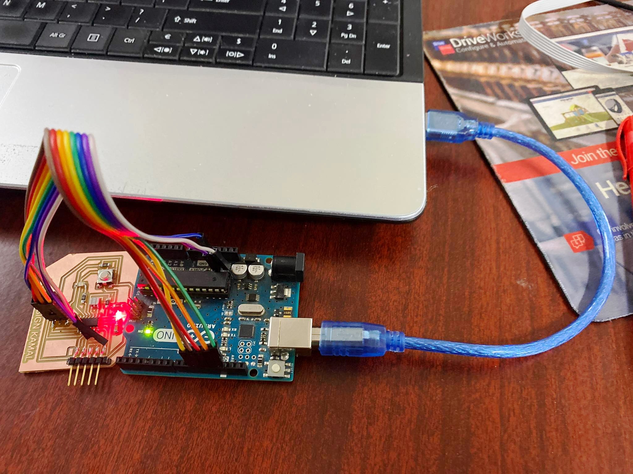
Initially I programmed the board with Arduino as ISP. This step is the more easier method to programing the attiny hello world board.
To Program the board using arduino as programmer, we first look at the pins connection between Attiny44 and Arduino board.
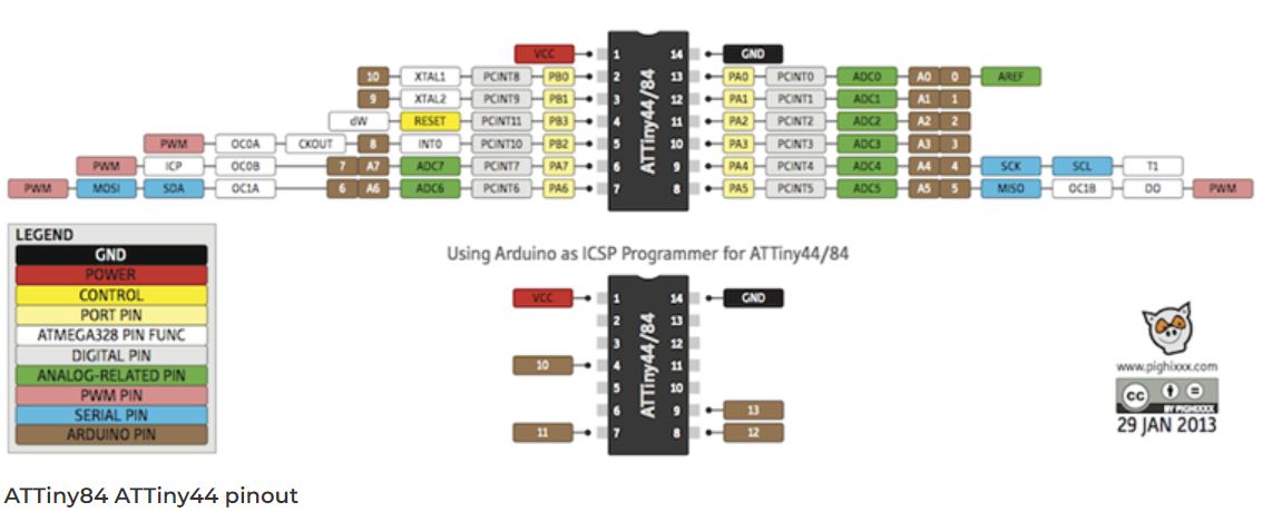
With the help of the pin diagram above, we make the connection to the arduino board and the hello world board. The arduino is initially used as a programmer to program the attiny hello world board.

We also choose the board to program. The board is initially not available on Arduino IDE. Therefore we have to download it from the internet and add it to the library of the IDE. In the Arduino IDE, we go to preference and add additional board manager URL. The file for the additional board manager is available on Github

With the json file added to the preference, the board will now be available on the board managers of arduino IDE.

With the board now available for programming and connections completed as required, we change the settings on the IDE as below:

Then we can use a simple blink LED program to check whether we can program the board or not. If the bootloader runs successfully without errors we can tell that the programming was successful, then we can check the functionality of the board. We can also add an input pin for the button such that, when the button is pressed, the LED will glow or any other function similar to that.
The blinking of the LED is shown in the video above.
Code Example of Blinking LED
// the setup function runs once when you press reset or power the board
void setup() {
  // initialize digital pin LED_BUILTIN as an output.
  pinMode(2, OUTPUT);
}

// the loop function runs over and over again forever
void loop() {
  digitalWrite(2, HIGH);   // turn the LED on (HIGH is the voltage level)
  delay(1000);                       // wait for a second
  digitalWrite(2, LOW);    // turn the LED off by making the voltage LOW
  delay(1000);                       // wait for a second
    digitalWrite(2, HIGH);   // turn the LED on (HIGH is the voltage level)
  delay(1000);                       // wait for a second
  digitalWrite(2, LOW);    // turn the LED off by making the voltage LOW
  delay(1000);
}
#define BUTTON 7
#define LED 8

int BUTTONstate = 0;

void setup() {
  pinMode(LED, OUTPUT);
  pinMode(BUTTON, INPUT);
}

void loop() {

BUTTONstate = digitalRead(BUTTON);

if (BUTTONstate == HIGH)
{
    digitalWrite(LED, HIGH);
    delay(20);
    digitalWrite(LED, LOW);
    delay(20);
    digitalWrite(LED, HIGH);
    delay(20);
    digitalWrite(LED, LOW);
    delay(20);
    digitalWrite(LED, HIGH);
    delay(20);
}
else
    digitalWrite(LED, LOW);
}
The demo of the above code is shown below:
Programming the Board with Fab ISP
Both the boards that we designed has six pin connectors that can communicate between the two in master-slave configuration. In this configuration, the ISP programmer we designed before will act as master programming the hello world board. The six pins are respectively using a SPI connector:
- MOSI
- MISO
- RST
- SCK
- VCC and
- GND.
We make use of SPI connectors we fabricated in lab to get the connections.
Addtionally, there is also need for us to provide a separate Vcc and ground to the HelloWorld board. The external supply has been provided from an Arduino board through the FTDI connection in the hello world board.

Care should be taken such that the connetions are properly made so that each pins on the FabISP are connected to the desired pin on the Helloworld board. I had made unique orientations of the SPI connectors in the Helloworld board so that the routing would go well. This complicated the connecting sequence a bit since the orientation of the two connectors was different. However, after properly checking the pins, I was able to properly make the connections of the two boards.
With the boards connected with each other, I proceed with providing the power supply to the board from an arduino board. The Power LED (RED) on the board signify that the board is powered. Initially the LED was not glowing therefore i went back to soldering board to check the soldering. The soldering was not properly connecting the FTDI connector with the the copper so i repaired that and had it working.
With the connections done i moved on to programming the board. Initially the programming was not working from windows so i downloaded a driver software for windows from https://learn.adafruit.com/usbtinyisp/drivers. After installing the driver, i connected the ISP to the PC using USB connection. Then was able to program the board. The code i programmed is shown below:
Program code of LED and Button controlled helloWorld Board
#define BUTTON 7
#define LED 8

int BUTTONstate = 0;

void setup() {
  pinMode(LED, OUTPUT);
  pinMode(BUTTON, INPUT);
}

void loop() {

BUTTONstate = digitalRead(BUTTON);

if (BUTTONstate == HIGH)
{
    digitalWrite(LED, HIGH);
    delay(60);
    digitalWrite(LED, LOW);
    delay(60);
    digitalWrite(LED, HIGH);
    delay(60);
    digitalWrite(LED, LOW);
    delay(60);
    digitalWrite(LED, HIGH);
    delay(60);
}
else
    digitalWrite(LED, HIGH);
    delay(20);
    digitalWrite(LED, LOW);
    delay(20);
}
Video: Working of LED blinking connected to push button.