7. Electronic design
Group assignment:
-
Use the test equipment in your lab to observe the operation of a microcontroller circuit board (in minimum, check operating voltage on the board with multimeter or voltmeter and use oscilloscope to check noise of operating voltage and interpret a data signal)
-
Document your work to the group work page and reflect on your individual page what you learned
Individual assignment:
- Redraw one of the echo hello-world boards or something equivalent, add (at least) a button and LED (with current-limiting resistor) or equivalent input and output, check the design rules, make it, test it. Optionally, simulate its operation.
1. GROUP ASSIGNMENT
This week we had a regional review at Fab Lab Esan and learned how to use instruments that help us measure voltage, amperage, ohms, connectivity, visualize noise and much more, you can see every detail below:
OSCILLOSCOPE
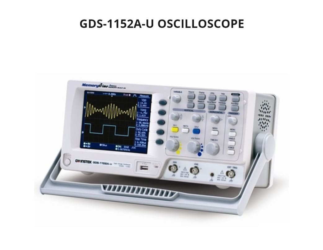
The oscilloscope model we have in the FAB LAB ESAN is: Instek GDS-1152A-U Oscilloscope
It is a general purpose 2-channel oscilloscope designed to meet diversfied educational demands and basic industrial requirements.
Features:
-
MANUFACTURER: GW Instek
-
TYPE : Digital
-
CLASS : DSO
-
BANDWIDTHS: 150/100/70MHz
-
INPUT CHANNELS: 2
-
SAMPLING RATE: 1Gsps (Real Time) , 25Gsps (Equivalent Time)
-
RECORD LENGTH: 2Mega Point
-
VERTICAL SCALE: 2mV -10V
-
HORIZONTAL RANGE: 1ns ~ 50s
-
Up to 27 Automatic Measurements
-
INPUT COUPLING: AC, DC, GND
-
TRIGGER COUPLING: CA, CC, high-pass, low-pass
-
INPUT IMPEDANCE: 1MΩ/15pF
-
USB Host and Device Interface Supported
-
Data Logger
How to use:
To make better use of the oscilloscope, these links will help you, a basic guide and the complete manual:
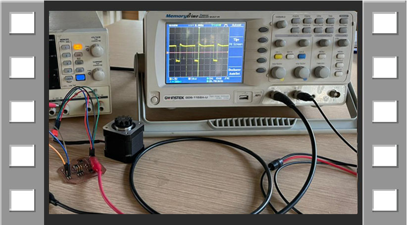
In order to test, the first thing I did was to connect a board that controlled a DC motor to a power source, because without it, it will not be able to send signals to measure the amperage or voltage behavior. Then I connected the board to the oscilloscope, I used CHANNEL 1, because CHANNEL 2 measured very small signals and multiplied everything x10.
Remember to connect the wires correctly, positive to positive and negative to negative, the power supply and the oscilloscope have clamps for a better grip and you can also use jumpers to make it easier to connect, that’s what I did.
Then, I clicked the OUTPUT button on the power supply and the oscilloscope screen began to show signals, these can be regulated in size, but that does not mean that the value of the signal is different, only its visualization.
On the display where it indicates Vmax 5.80V, we will take it into account to compare with the multimeter.
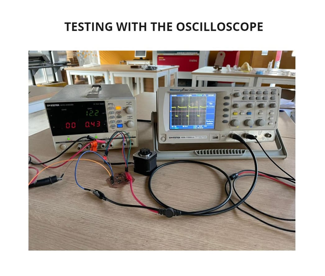
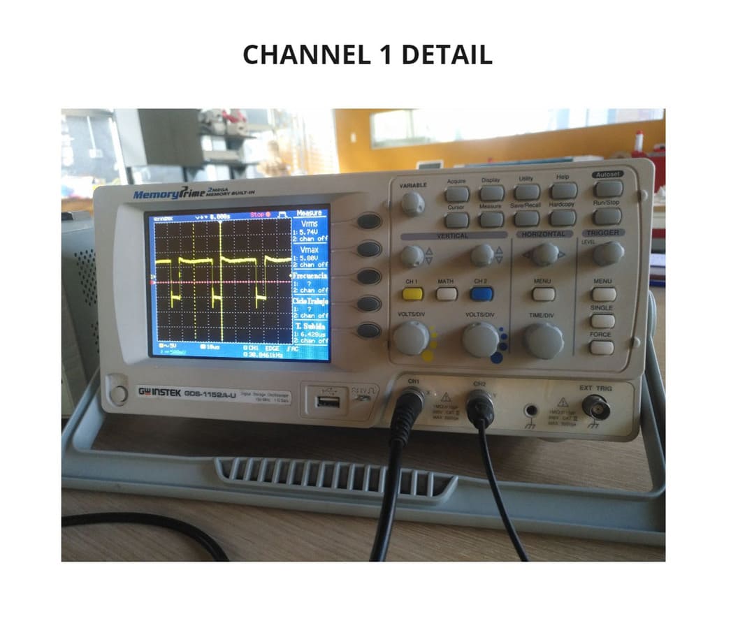
To visualize the signals well, remember to make the correct configuration, the gray buttons on the side of the screen are used to configure well what is being measured, whether it is a digital or analog signal.
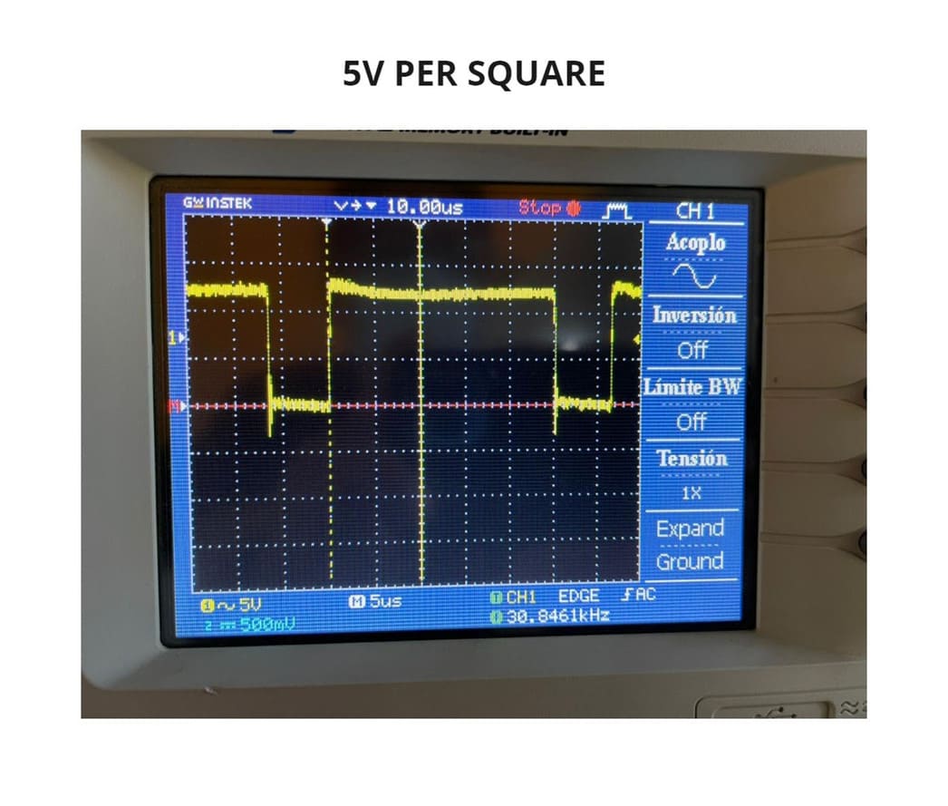
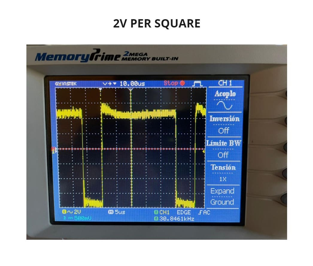
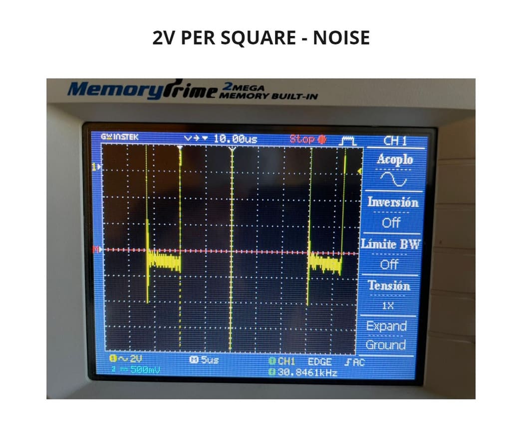
One thing I did to measure better was to move the signal to the red line. When ~5V appears at the bottom, it means that each vertical square has 5V. In the first image you can see that the signal occupies 2 and a half squares, it means that it has about 12 to 12.5V approx. and there are noise signals protruding at the ends.
To see better, we enlarge the screen and now each square has a value of 2V, there we see that there is a noise signal that occupies almost a full frame at the top, while at the bottom there is a peak that occupies 2 frames, which means it has almost 4V, it is also called eddy current and is something that usually happens with the DC motor we are using for testing.
Something that can also be observed is the measurement of 30.8461kHz, it indicates the frequency, cycles per second that this signal repeats. This can be measured horizontally, 6.2 squares approx. are used, the signal starts and the same thing is repeated over and over again.
VIDEO

DIGITAL MULTIMETER
Digital multimeters combine the testing capabilities of single-task meters—the voltmeter (for measuring volts), ammeter (amps) and ohmmeter (ohms). Often, they include several additional specialized features or advanced options.
At FAB LAB ESAN we have different multimeters, but the one we will mainly use is the PRASEK PR-301C model. It is capable of measuring voltage, amperage, ohmmeter, diodes and continuity.
Features:
-
DC VOLTAGE (V): 200mV / 2000mV / 20V / 200V / 500V
-
AC VOLTAGE (V): 200V / 500V
-
DC CURRENT (A): 2000mA / 20mA / 200mA / 10A
-
RESISTANCE (Ohm): 200 Ohm/2KOhm / 20KOhm / 200KOhm / 20MOhm
The test leads are flexible insulated wires (red for positive, black for negative) that are connected to it. They act as the conductor from the material under test to the multimeter. The test leads of each cable are used to test the circuits.

How to use:
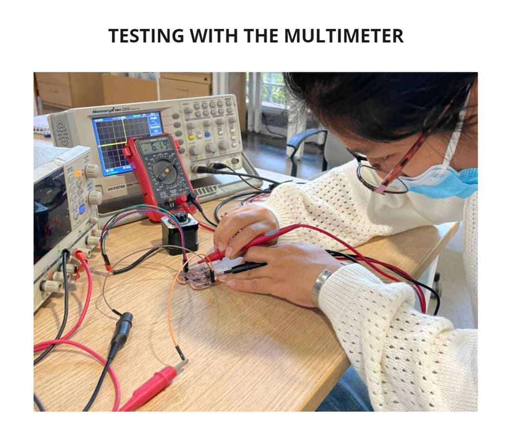
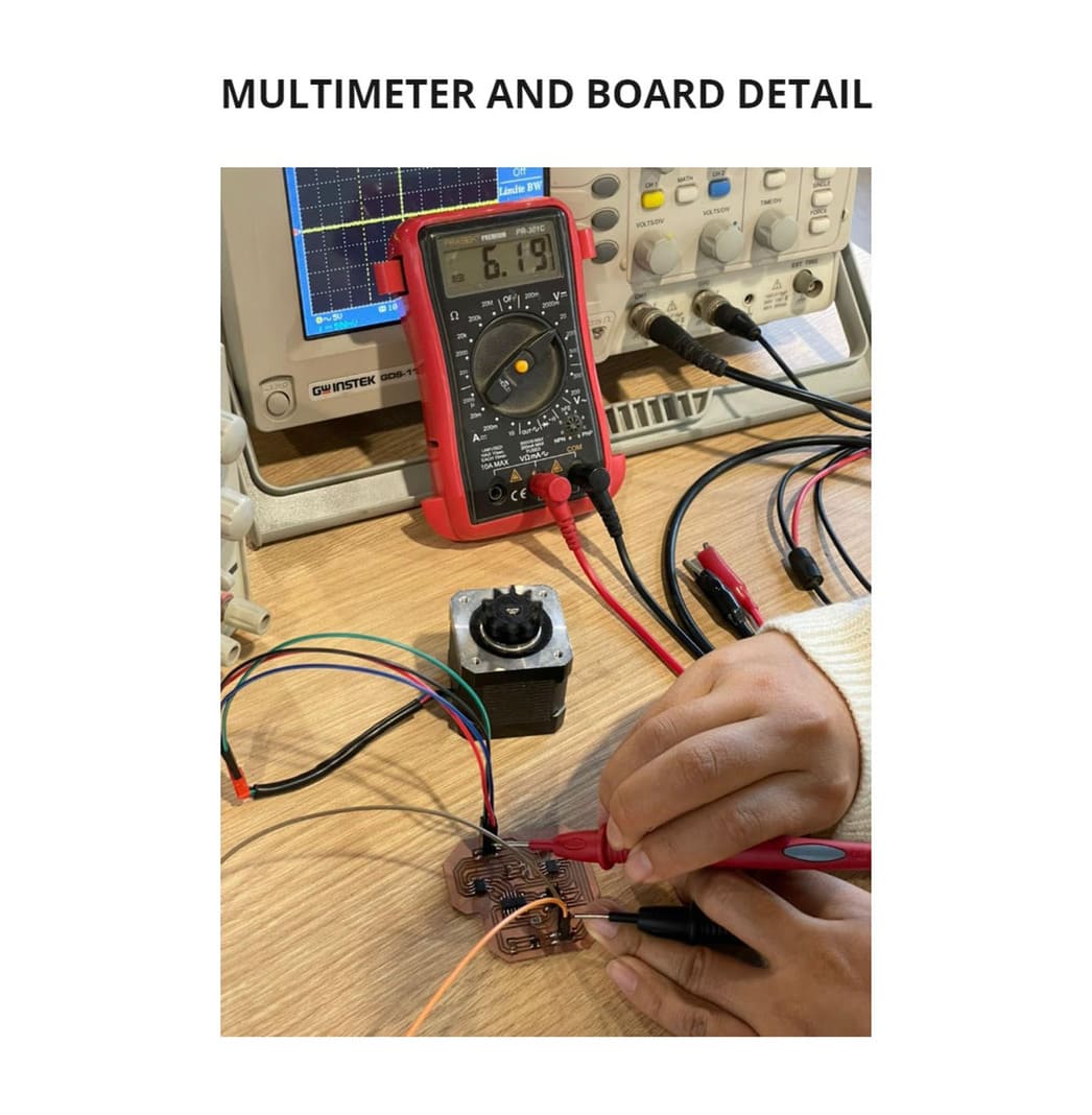
Using the same board I used with the oscilloscope, I decided to measure Voltage, so I turned the multimeter arrow to 20V (since the power supply indicated 12V and is in that range).
Place well the tips of the positive and negative wires, I obtained as a result 6.19V. Something similar that happened on the oscilloscope screen where Vmax indicated 5.80V, a value almost similar, but different from the 12 V that was seen on the power supply and the signal graph. This may be because it is the voltage rises and falls in a very short period of time and its stable value is 6.19V.
As a side note, you can also see the continuity of the components on a board by placing a tip of the clamp at each end, the components must share the same path that connects them. A sound will be emitted if there is a connection, but if there is no sound it means that there is no connection and you must verify that it is well soldered.
Finally, you can also measure the ohms of a component or know the positive or negative of a LED (if it lights, it means it is connected like this: black = negative ; red = positive, this way you can place the component well on the board), this you can see more in detail in my individual assignment, as I had to use this tool to identify mistakes I was making.
2. INDIVIDUAL ASSIGNMENT
This week our instructor trained us in the operation of basic electronics and the use of EAGLE, especially for those of us who have never seen these topics. This way we are not only redraw a board for individual assignment, but also understanding how it works.
DESIGN
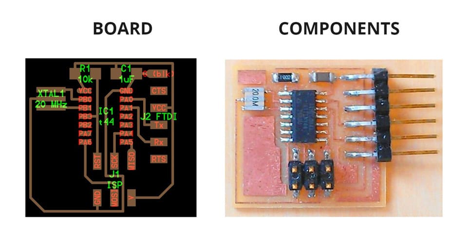
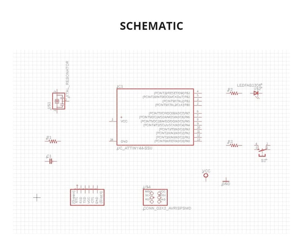
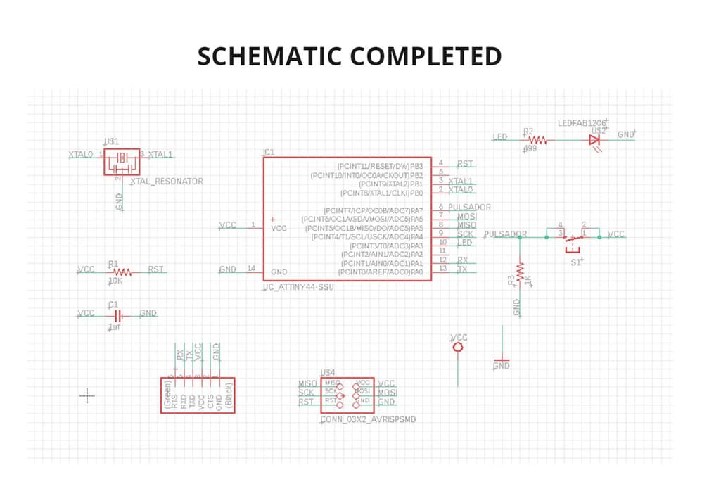
I redraw one of the echo hello-world boards, I chose the one with an Attiny 44 microcontroller and also added a button and led to the design.
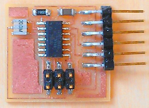
Before I start, I show you the example board I used as a guide:
Unlike the week we looked at electronic production, this time we got to design from scratch and I chose EAGLE (program).
WHAT IS EAGLE?
EAGLE is a scriptable electronic design automation (EDA) application with schematic capture, printed circuit board (PCB) layout, auto-router and computer-aided manufacturing (CAM) features.
In order to design my board, I performed the following steps:
-
Install EAGLE, create your user with your password and email. In my case I have an educational license.
-
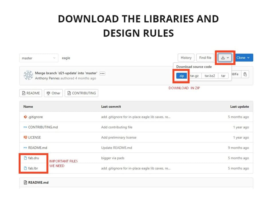
The program comes with a default library, but you will need the library provided by the Fab Academy to continue, as well as the design rules, both can be found in the following link: EAGLE DESIGN RULES AND LIBRARIES.
If you use other software, you can find the libraries here:ELECTRONIC LIBRARIES AND DESIGN RULES.
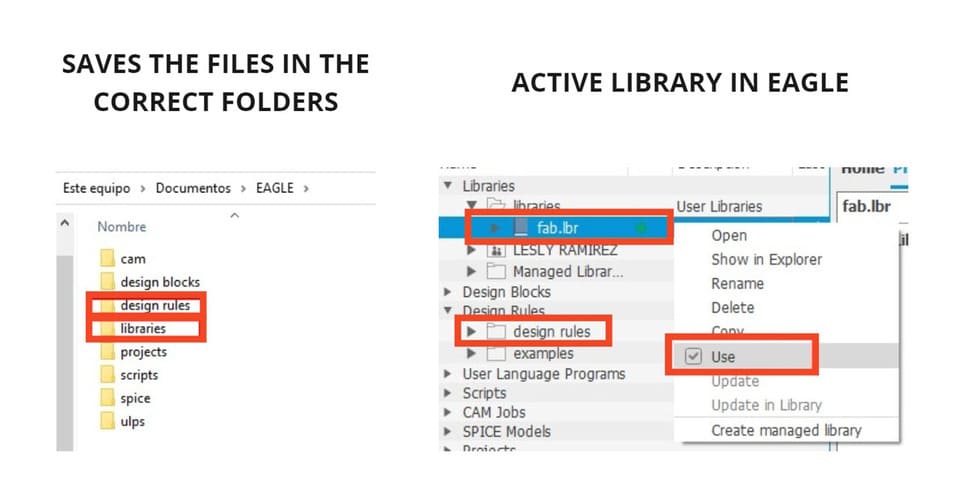
- When the program is already installed, a folder with the program name will appear and there you must copy each corresponding file:
FAB.DRU in the folder of Design rules y FAB.LBR in the folder of Libraries
I am detailing each step so I can remember when I make more boards for next assignments. I didn’t know anything about electronics before, during the Fab Academy I am learning a lot. 😅
-
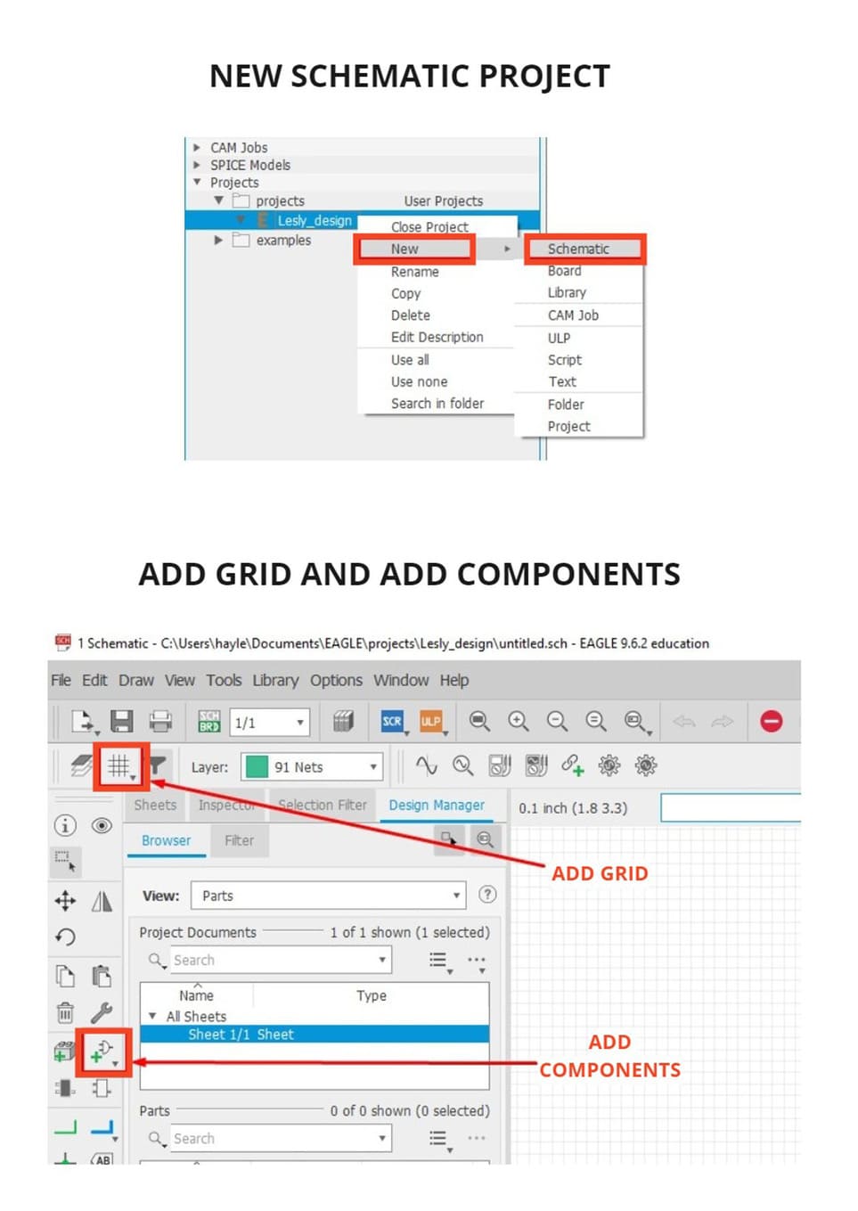
On the main page, click on
projects>NEW PROJECT, then you can rename it I called my projectLesly_designand secondly you must create the schematic, click onLesly_design>NEW>SCHEMATIC. -
A new window will open and I recommend you to activate the GRIDS and then start adding the components you will need.
-
To find the components, you go to the
FABlibrary and choose what you need. I chose my first component which is theATTINY 44, in the images below you will see how it is displayed schematically and the details.
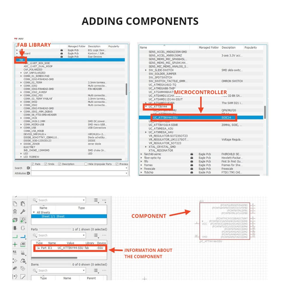
- Here is the list of components I used and the names under which you can find them in the library:
UC_ATTINY44-SSU
GND
VCC
CONN_03x2_AVRISPSMD
CONN_06_FTDI-SMD-HEADER
SW_SWITCH_TACTILE_6MM6MM_SWITCH
LEDFAB1206
CAP_UNPOLARIZEDFAB : C1 - 1 uF
R1206FAB : R1 - 10K
R1206FAB : R2 - 499
R1206FAB : R3 - 1K
XTAKL_RESONATOR
-
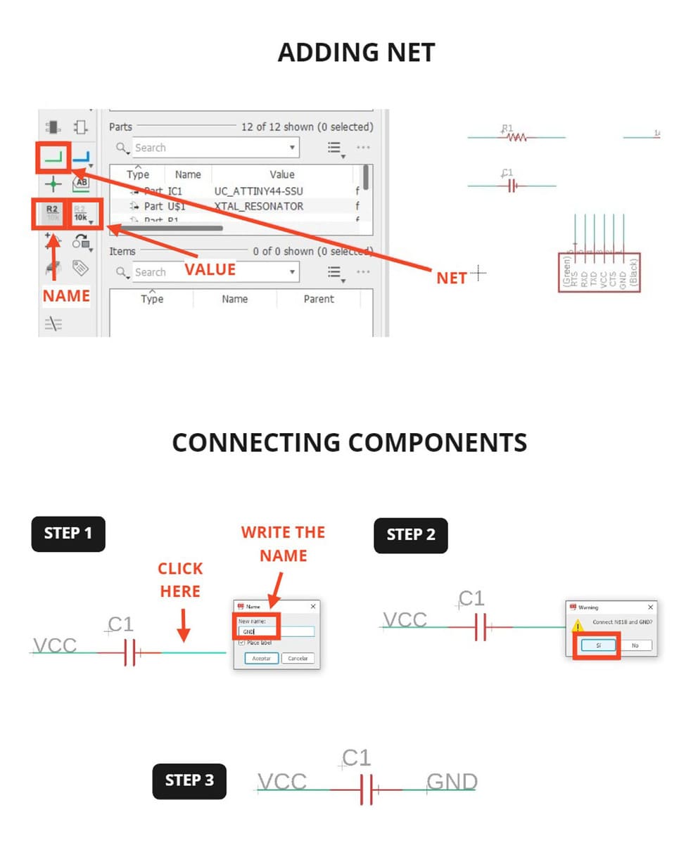
After you add all the components you will have the schematic almost ready, you must add a
NETthat helps to join the components and to create the board design, you can locate it in the shape of an invertedLand in green color in your toolbar in EAGLE. -
You should also name it with the
NAMEtool, this way those with the same name will be able to join, for example: ARESISTORhas connection forGNDandVCC, each side will be able to connect to another component that has the same names added.
Keep in mind that it does not come together randomly, in the FAB LAB ESAN node we had a class on how electronics components work and how they should work together.
- Finally, you must also add a value with the
VALUEtool if it is necessary, I added different sizes for theRESISTORS, since I had10K, 1K and 499, in the case of theCAPACITORI had1uF.
This way you will have your schematic design ready!
-
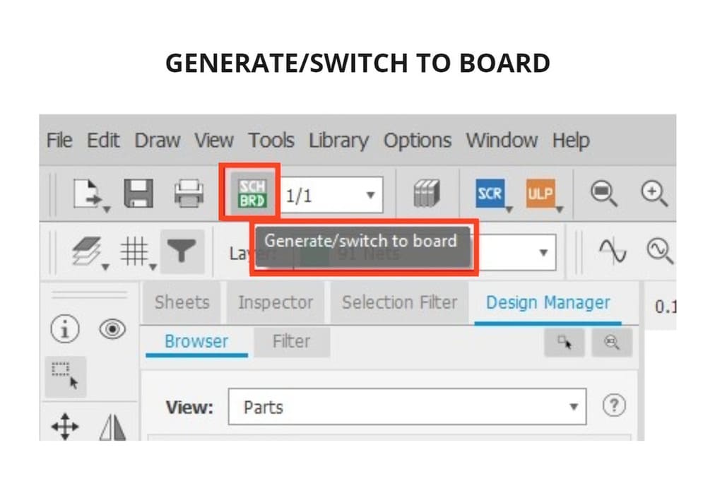
Now we have to generate the design of the board and how it will look like in reality, so go to the
GENERATE/SWITCH TO BOARDtool. -
A new window will open with the components and their
FOOTPRINT, which is the pattern you will have to follow for joining and soldering, but the first thing you will see will be a bit messy and you will have to work from there. -
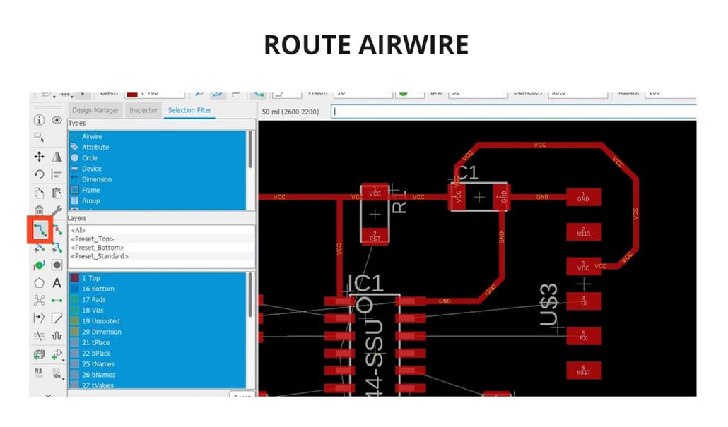
You have two ways to join everything together, the first option is to use the
ROUTE AIRWIREin which you have to manually join component one by one. To make the connections you must take into account the following:
LAYER: TOP
WIRE BEND : Inverted L (see the image below)
WIDTH: 16
By using the Wire Bend with the proper shape, it will help make the wires less likely to be bumped or ruined during milling or welding.
-
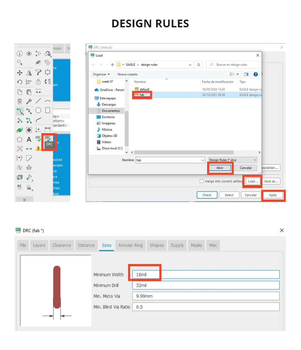
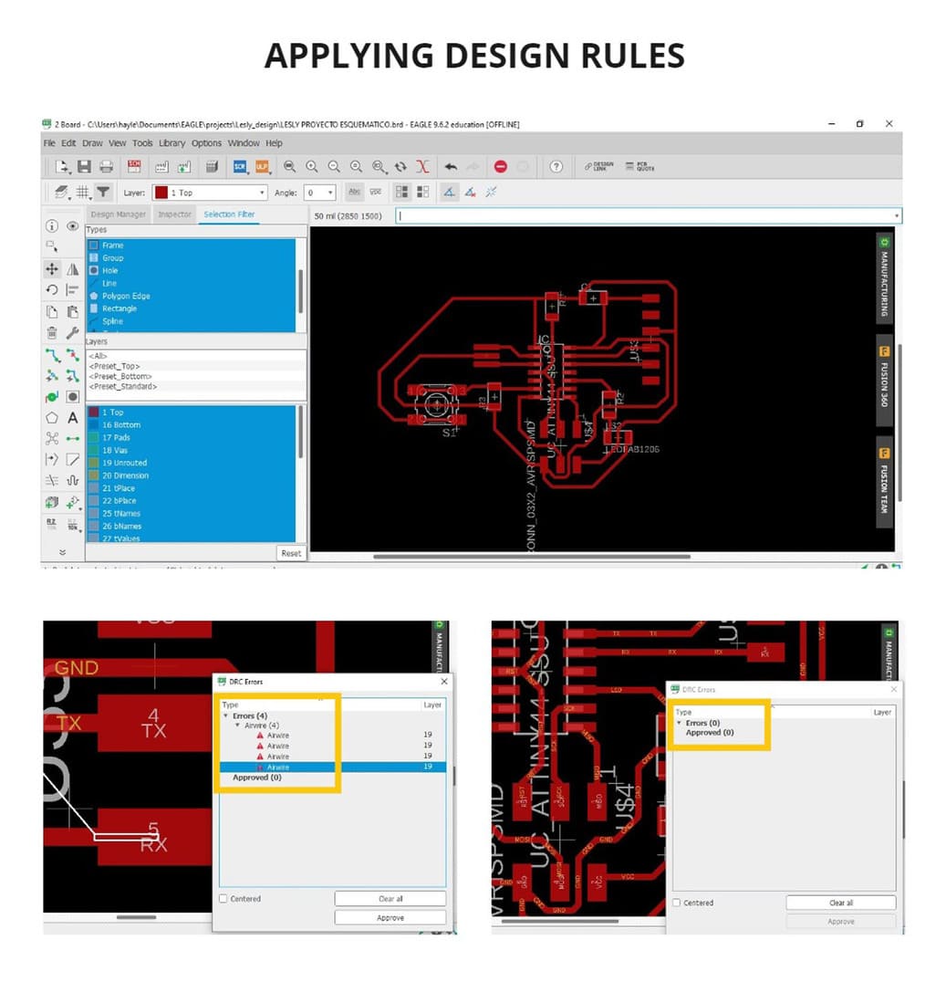
Something to keep in mind is to have the
DESIGN RULESloaded, in this case I am usingFAB.DRU, to apply them you must click on:DRC>LOAD>FAB>OPEN>APPLY. -
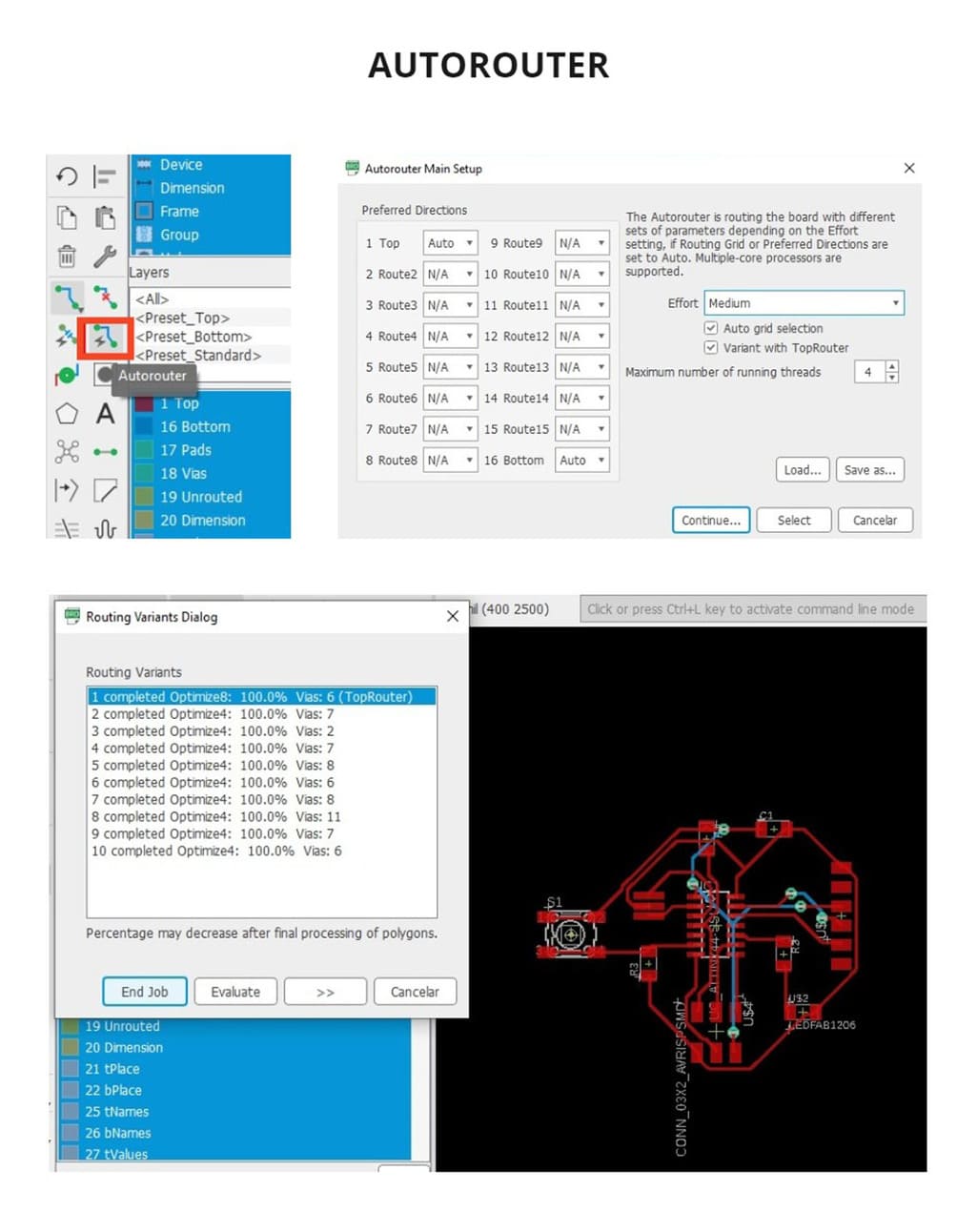
You also have the option of the
AUTOROUTER, which connects the wires by artificial intelligence, but if you do not know how to configure it correctly, the same thing can happen to you as it did to me, the program created joints with holes as if it was going to drill the board.
I followed so many times these steps that in the end I left it, I started to join everything with the ROUTE AIRWIRE.
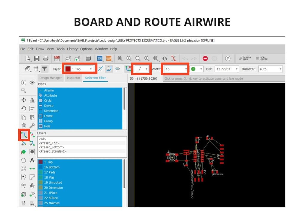
-
Using the
ROUTE AIRWIREtool helped me to better organize each wire. At some point it looked like nothing was going to work because the spaces were so tight, but I managed to connect all the wires. -
At this point I only had to confirm that everything was OK by applying
DESIGN RULESand I got 4 errors, missing lines that had not fully reached their destination, they were so tiny pieces that I had to see one by one and in the end I gotERRORS(0). -
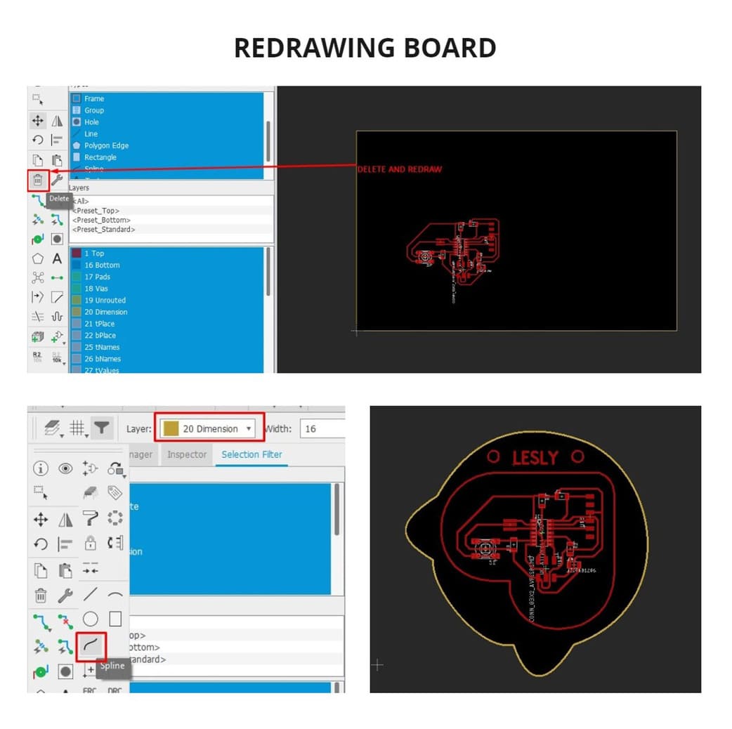
The only thing I needed to do was to draw again the border of the board, since the one shown was giant. I erased the edges, chose the
DIMENSIONlayer that has a yellow color, used the same thickness16, but this time I used theSPLINEtool to make curves and achieve the final shape. -
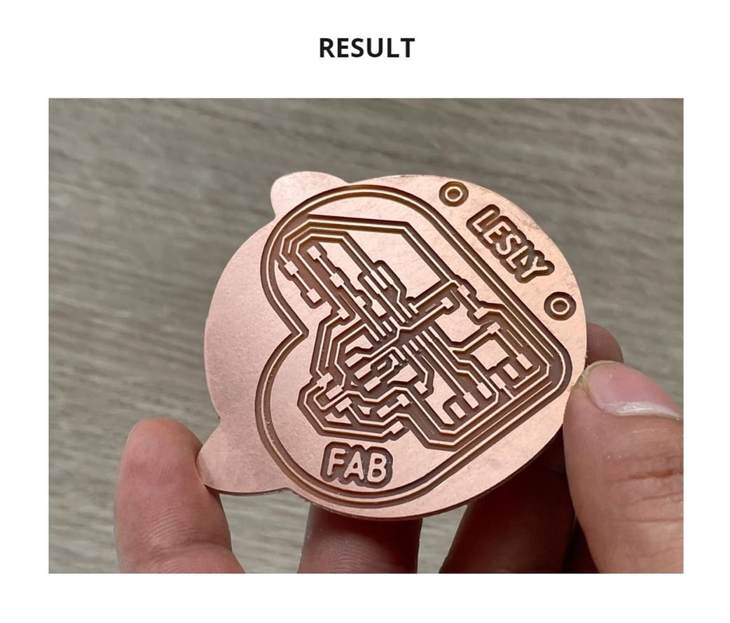
You can also add text, I added my name
LESLYand the wordFAB, on theTOPlayer so that it is engraved and not cut. -
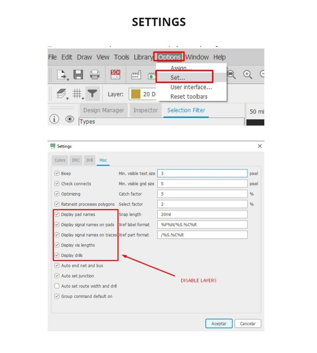
In order to continue, you must export the strokes and edges separately, so you must first disable the elements that should not be displayed. First go to
OPTIONS>SETTINGSand disable the layers:
Display pad names
Display signal names on pads
Display signal names on traces
Display signal names via lengths
Display drills
-
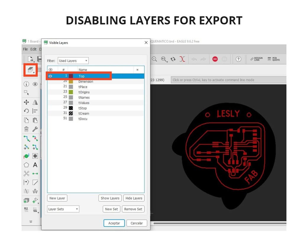
Finally, you must deactivate some layers in the
LAYERStool and only leave active the one that will be used. For example, to export the strokes, you should only have theTOPlayer active, while to export the border, you should only have theDIMENSIONSlayer active. -
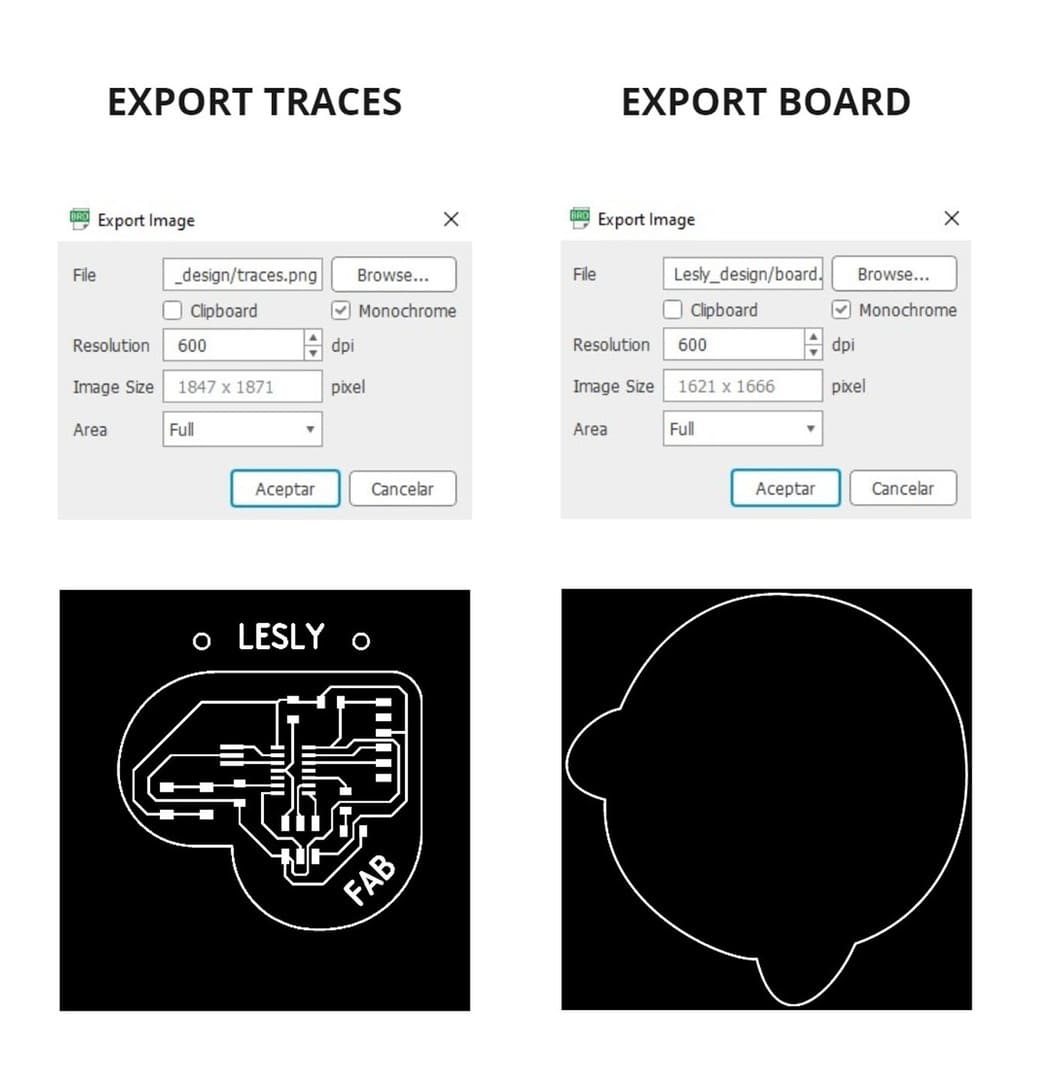
Remember, when exporting the image you must choose the path where it will be saved, the name it will have and its specifications, I recommend you to choose:
MONOCHROME
RESOLUTION: 600 DPI
And that’s it, your design is ready to be made!
FABRICATION
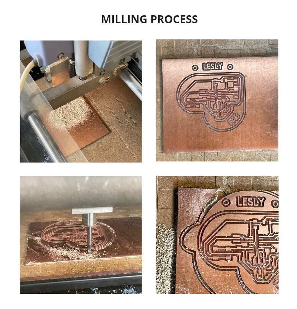
For fabrication I followed the same steps for using the Roland Modela MDX-20 milling machine on Electronic production’s week. The milling cutters used are the same, 1/64'' and 1/32'', as well as cutting and milling configurations.
You can see it in the following link: Milling Machine configuration
During the milling process, one of the most difficult parts was locating the design inside the cooper plate, as it was large and curved.
The design was so close to the edge that it was almost ruined when cutting, it lifted slightly during the cutting process, I was lucky because a milling cutter might have broken and there are not many spare parts available at the moment.
The final result was very good, the FOOTPRINT was connected correctly. If you see any lines that look broken, they are not part of the wiring, they are the debris that comes out when the engraving is done and surrounds the FOOTPRINT.
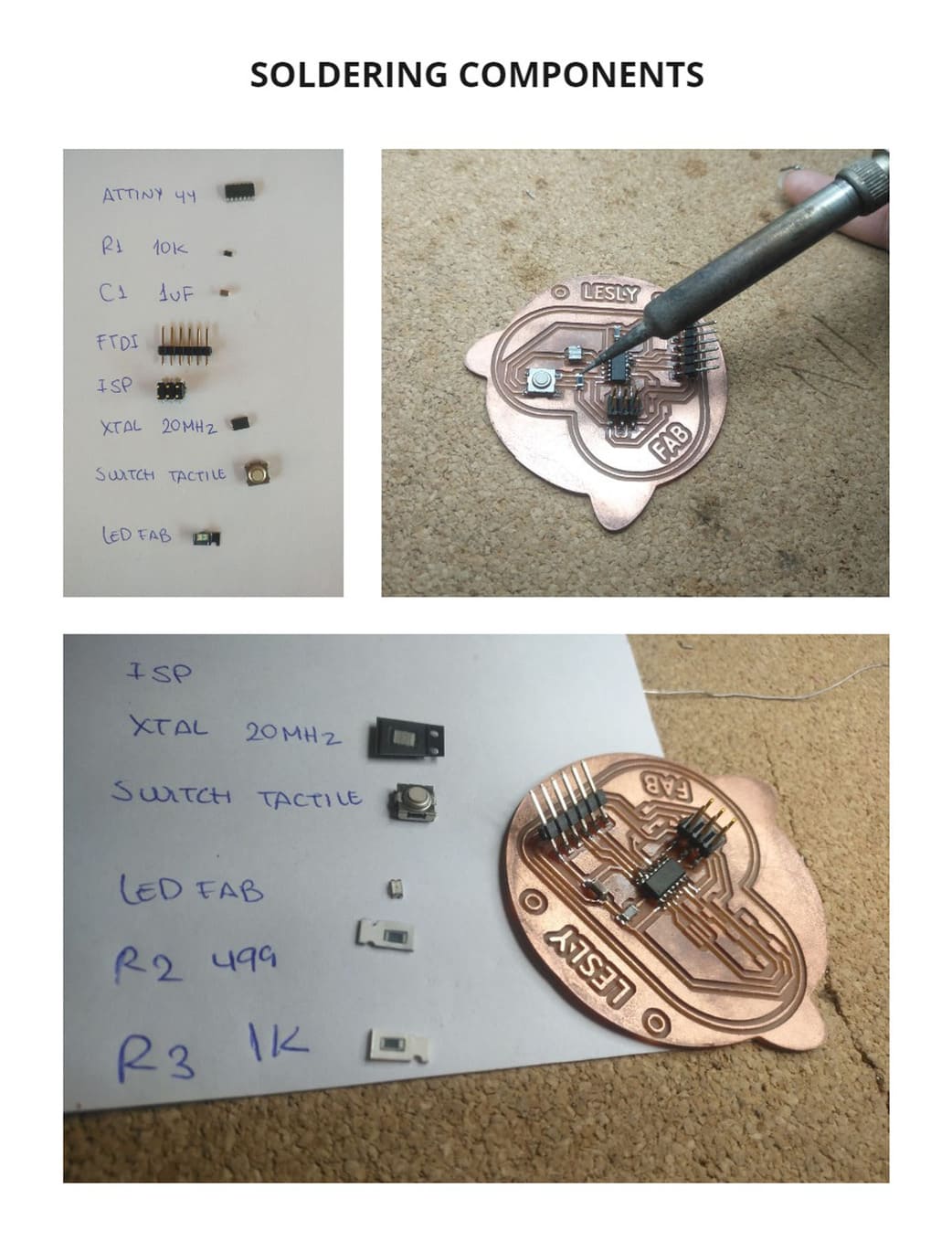
SOLDERING COMPONENTS
In order not to lose any piece, I placed the name of each one and the component next to it, there were pieces so tiny that I had to use a tweezers to be able to solder them.
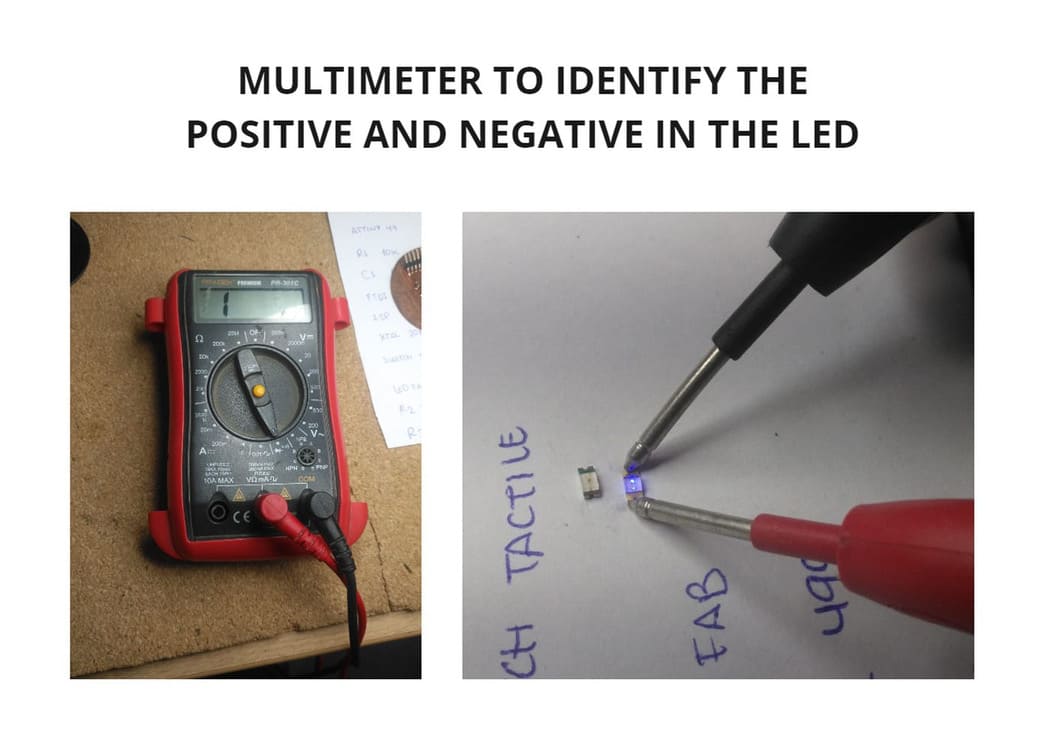
Something to keep in mind is the position of some parts, in this case for the LED I had to use a multimeter and locate the positive and negative. This is because the negative has to be attached to GND.
To confirm that each side is correct, the LED will light when the black clamp of the multimeter is with the negative and the red with the positive. This way I was able to locate and solder my LED correctly.
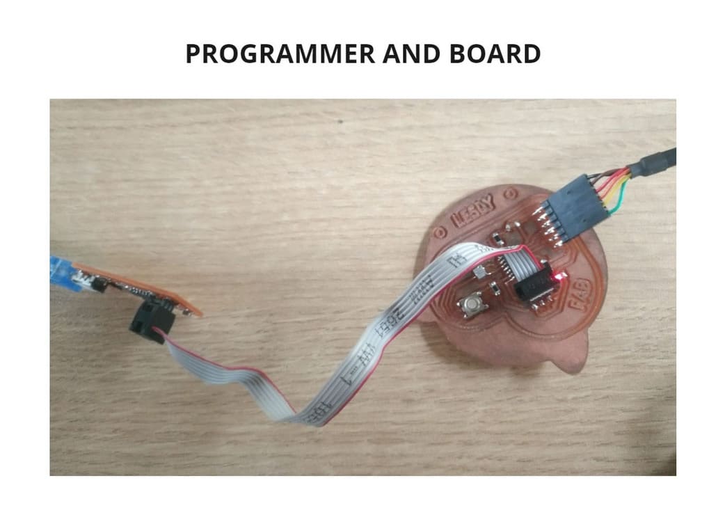
I finished soldering all the components and tried to record a code using ARDUINO IDE, connecting the programmer to the board and the computer, but as soon as I connected it, the LED turned on for no reason, it was not even programmed.
I checked again that everything was well soldered, there were components that I had not soldered well, so I solved it and I also checked with the multimeter that there was a connection between all the components that were related.
Again I reconnected the board to the programmer and the pc, this time the LED did not turn on at the contact, so I used ARDUINO IDE to program and it did not work, the LED did not turn on when I pressed the PUSH BUTTON.
WHAT HAD GONE WRONG? WAS SOMETHING SOLDERED WRONG? WAS SOME COMPONENT BURNED? DID I PLACE THE WIRES WRONG? All these doubts running through my head and I didn’t know what hadn’t worked, so when I tried to disconnect and connect too many times, the FTDI came off the board, including copper parts 😢.
It was very difficult to join it, but it was achieved, I put tin to rejoin the FTD I to the board and for the part of the copper connection that broke, I managed to join the ends of a wire to the board using tin, something similar occurred during the Electronic production’s week and as a reinforcement I placed silicone to prevent another accident.
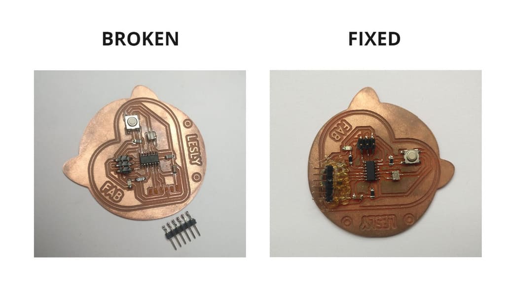
I repeated the same steps to program, but nothing worked, I checked the design in EAGLE several times, I even changed the operating system from Windows to Linux… I didn’t know what to do, so I made another board the same way, re-milling, re-soldering and trying to program again, but this message appeared again:ERROR.
My instructor suggested me to check if any component was incorrect or if it didn’t have the characteristics it should, that’s where I found the root of the problem. I used the multimeter to measure the value of the components, the resistors come in a long strip, so in order not to have to remove a component from the board, I measured a resistor from the same strip where I had taken it from and guess what was the surprise.....
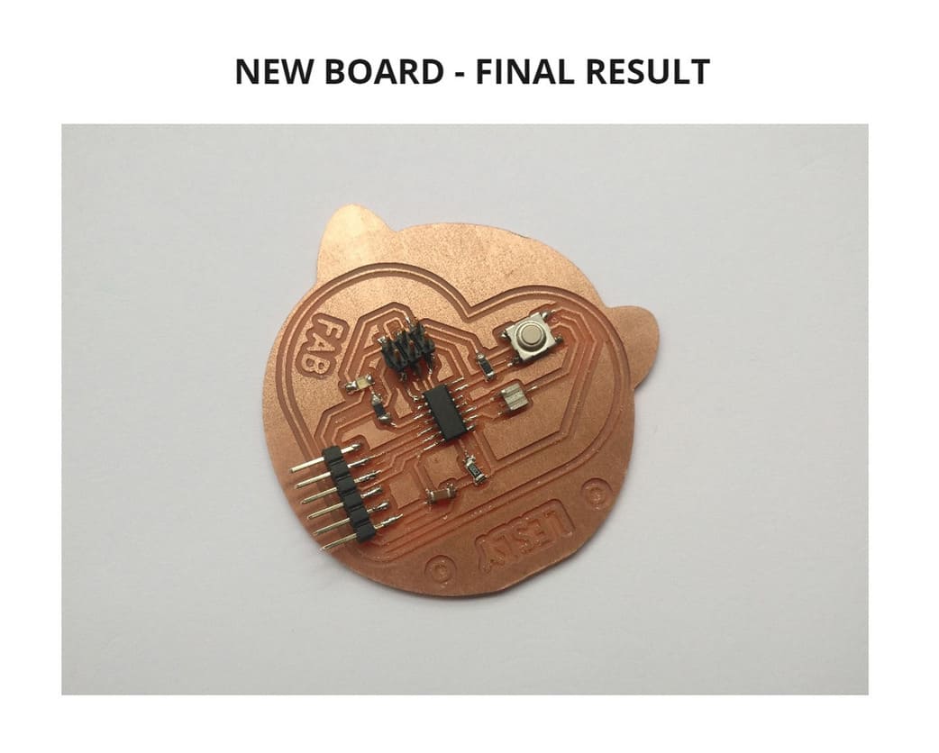
the resistor had 0.5 instead of 10K, that was the error and I hoped it was the only one. So, I removed the old resistor and put in the correct 10K resistor, set the code to EAGLE, tried programming one more time and IT WORKED!
This just means that the previous board was well designed and well soldered, the error was an incorrect value component, that’s why it is important to check components before soldering. One thing I noticed is that the 10K resistor had numbers on its outer design, while the 0.5 had nothing.
PROGRAMMING
To perform the test I used the following code in ARDUINO IDE:
#define led 3
#define pushbutton 7
void setup() {
 // put your setup code here, to run once:
  pinMode(led, OUTPUT);
  pinMode(pushbutton, INPUT);
}

void loop() {
  // put your main code here, to run repeatedly:
  if (digitalRead(pushbutton) == HIGH){
    digitalWrite(led, HIGH);
  }
  else{
    digitalWrite(led, LOW);
  }
}
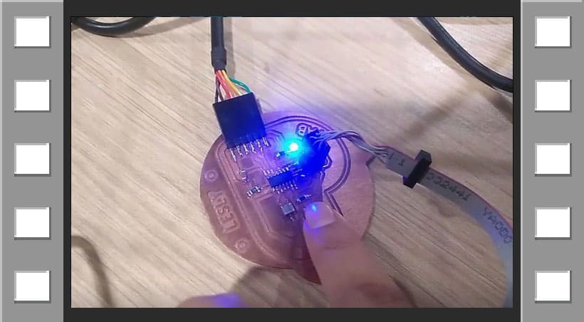
And this was the result:
VIDEO

3. CONCLUSIONS
-
Knowing the correct use of equipment such as a multimeter or oscilloscope will help you identify errors easily.
-
You have to check if the components have the corresponding value like ohms, amperes or voltage, you can check with the multimeter if there is connection between components that are in the same path or if they have the correct value.
-
If any path on the board is broken, you can use a copper wire to join it and solder it to the board.
-
Be careful when removing external connections, e.g. you can press on the component and remove the wiring slowly.
-
Linux is the operating system with the best adaptability for programming, sometimes Windows has problems with updates.
-
Keep in mind to apply
DESIGN RULESto verify that your board design does not have any faults in the program you are using. -
Advance your project and document in parallel at least with annotations, it will help you not to forget important details, especially of a subject that you do not know very well. If you have doubts, consult your instructor and always check additional information.