Final Project
Week 0: Digital Fabrication Principles and
Practices
Week 1:
Collaborative Technical Development, Documentation and Project
Management
Week 2:
Computer Aided Design
Week 3:
Computer Controlled Cutting
Week 4:
Electronics Production
Week 5:
3D Scanning and Printing
Week 6:
Electronics Design
Week 7:
Moulding and Casting
Week 8:
Embedded Programming
Week 9:
Computer Controlled Machining
Week 10:
Input Devices
Week 11:
Composites
Week 12:
Interface and Application Programming
Week 13:
Output Devices
Week 14:
Networking and Communications
Week 15:
Mechanical Design and Machine Design
Week 16:
Applications and Implications
Week 17:
Invention, Intellectual Property and Income
Week 18:
Project Development
Week 19:
Final Project Presentation
|
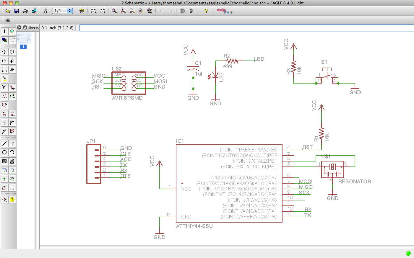
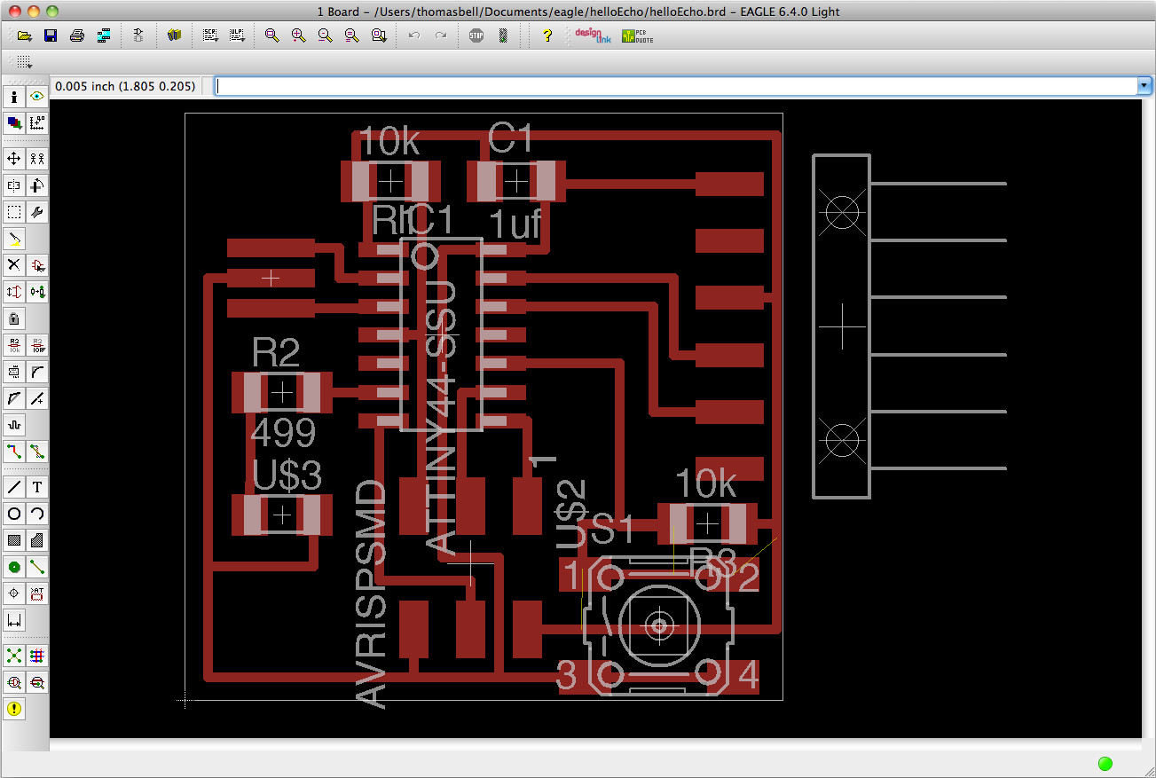
Electronics Design
For
this
week the assignment focussed on the design and the production of the
hello world circuit board. The most appropriate method of doing
this was by designing the schematic and then the board layout in Eagle and then creating a
.png file from the traces and then using the
necessary milling software to create the board as we have done in a previous week. Following Anna's tutorial
it was simple enough to import the required fab and component
libraries, and put together a schematic that included the basic
hello-world board plus the additional switch and LED necessary.
Using Eagle:
By making nets (links)
between components you connect elements on the schematic without a
physical connection as long as they are labelled the same within the
schematic, this can create a less cluttered schematic workspace, but
you should remember to keep track of which parts are connected,
otherwise the schematic can become slightly convoluted and choatic.
To create the board layout, I followed Anna's layout and manually
routed all the traces, using the tolerances in the program (i.e 16mm)
to ensure that the traces weren't too close together. Once I had
iteratively developed the traces to the most compact area I could, I
ran the design rule check within Eagle to ensure that the circuit ran
correctly. I received several warnings, as certain components
didn't have a value (i.e. the switch) but this was ok, because they
didn't impact on the functioning of the circuit.
|
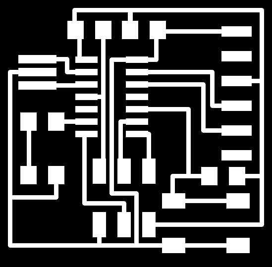
I
exported the traces as a .png image at 500dpi from Eagle and then
imported them into the milling software VCarve, which this lab has
already preinstalled as the router is not set up to use with the Fab
Modules. Once I Imported the .png image, I created vectors
from the image and then milled the board. Unfortunately, my first
attempt the board was not completely flat on the bed and was not milled
correctly.
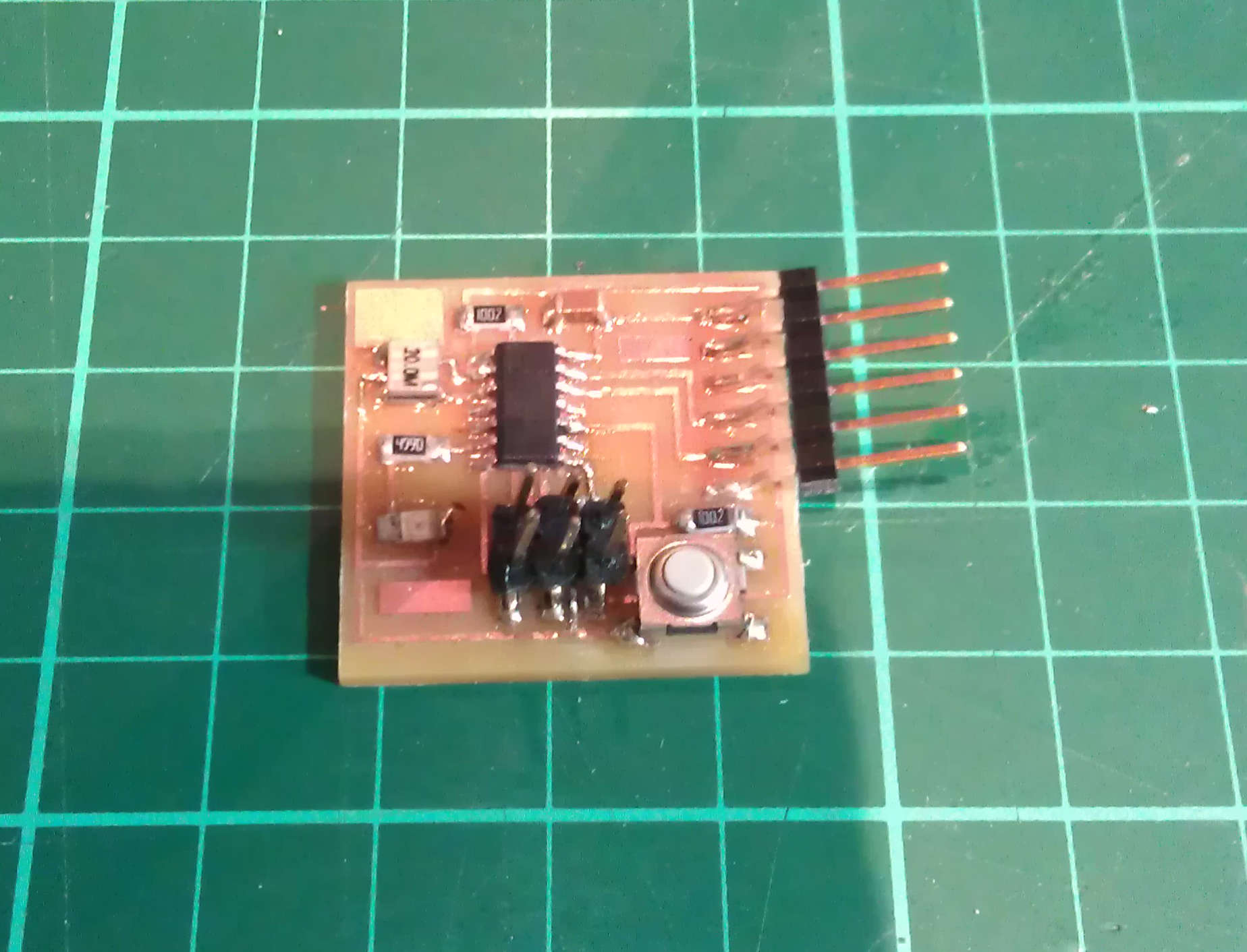
The
second attempt of milling worked out perfectly, and I began stuffing
the board. Be aware that the LED is still a diode and will only
accept current in one direction, I had to remove the LED after
forgetting this! Also, ensure that for the FTDI header solder the
single pad last, as it had a tendency to remove the pad completely if
you solder that pad first. For the AVRISPSMD, I had to create the
header pins from separate header pieces and solder them on
individually, this can be done but it is not recommended!
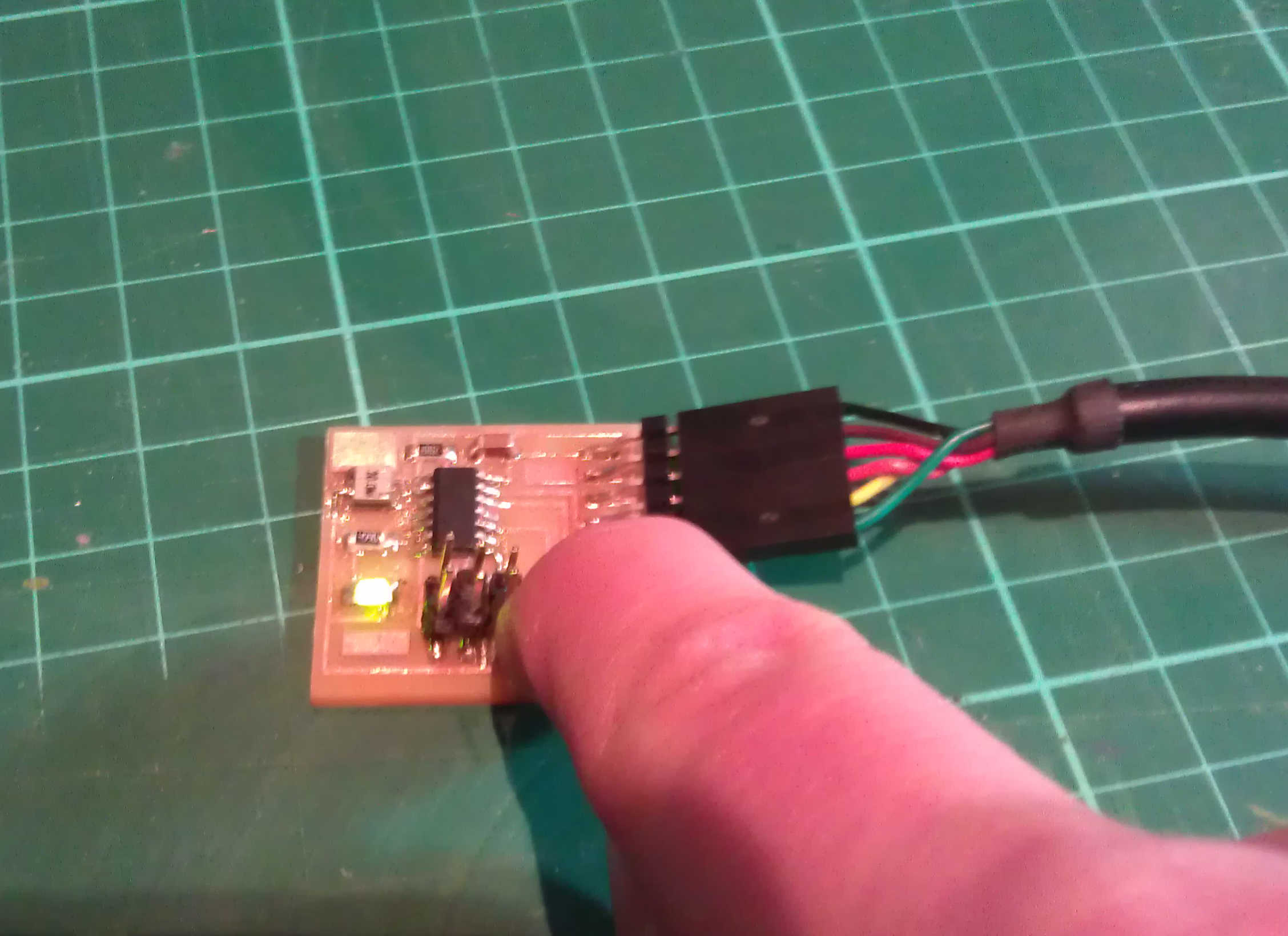
After, I had finished stuffing the board. I ran a program on the
board that was provided by our Guru, this was a simple program to
ensure that the board worked. I installed this using the AVR programmer
we used in the previous week to program our FabISP and made sure there
was power to the board using the USB into the FTDI header. The
simple program shone the LED when the button was pressed, the board
worked first time.
|