This assignment it cannot finish the manufacture my microcontroller for my drum because I had a problem in the milling of my board, also this week my country Peru, the government quarantined the whole country until further notice due to the problem
COV-19, so the manufacturing would still be pending.
But if I can manufacture and program the
Hellow world circuit for do my PCB designs I use online software
EasyEDA and
FlatCAM, For me this is a simple sofware and are simple to use and learn. I use these electronic components: One microcontroler ATTiny 44, two ISP conections, 01 resistance R1K and one red LED. Below are the steps of my process.
-Hello World board-
STEP 0. In the schedule they give us an image (Picture Base) where they show a design of a HelloWorld PCB so that we can guide ourselves and design a PCB with our own design.
Picture Base.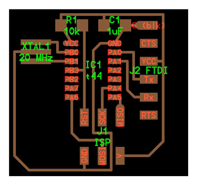 STEP 1.
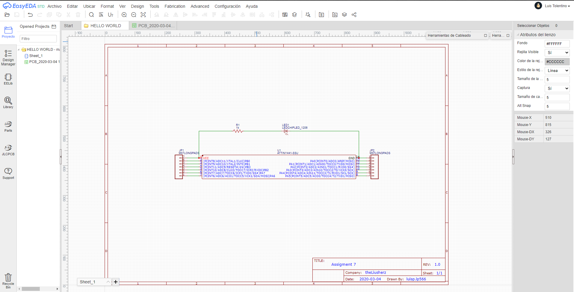
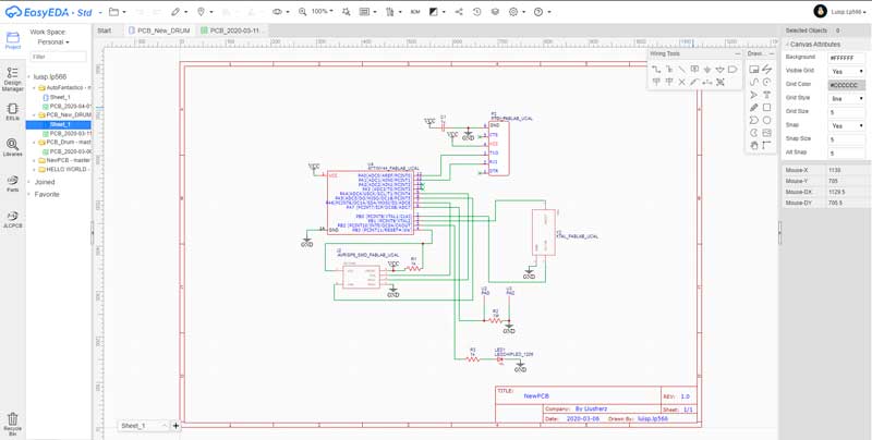
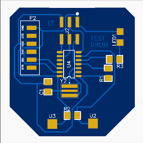
 I design and draw in
EasyEDA my own HelloWorld PCB following what my instructor taught me. This was an experience in PCB design that I really enjoyed and it was easy to do.
Picture 72.0. In this image I show my design of my schematic that I made in
EasyEDA .
 Picture 72.1.
 In the picture below, I show my design process of my PCB.
 Picture 72.2.
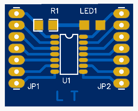
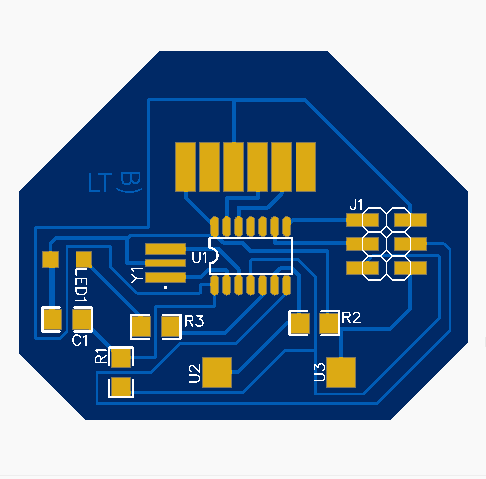
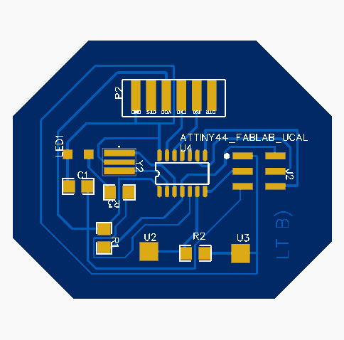
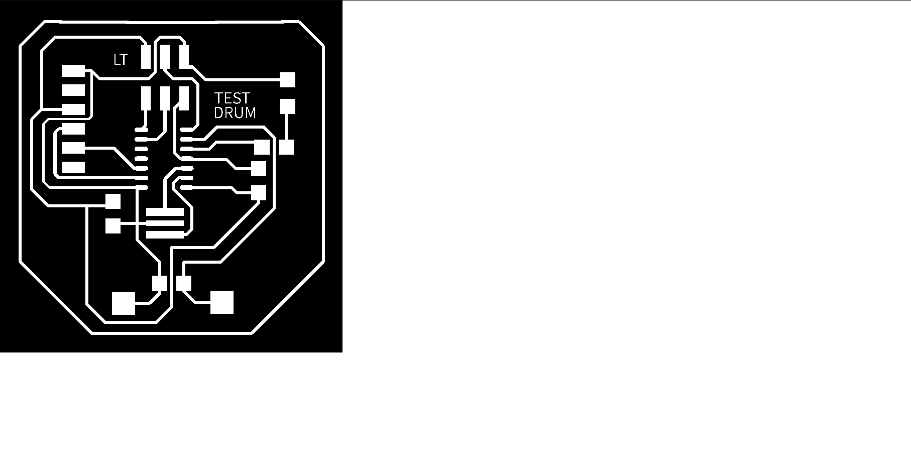
 In the image below I show my final design of my PCB.
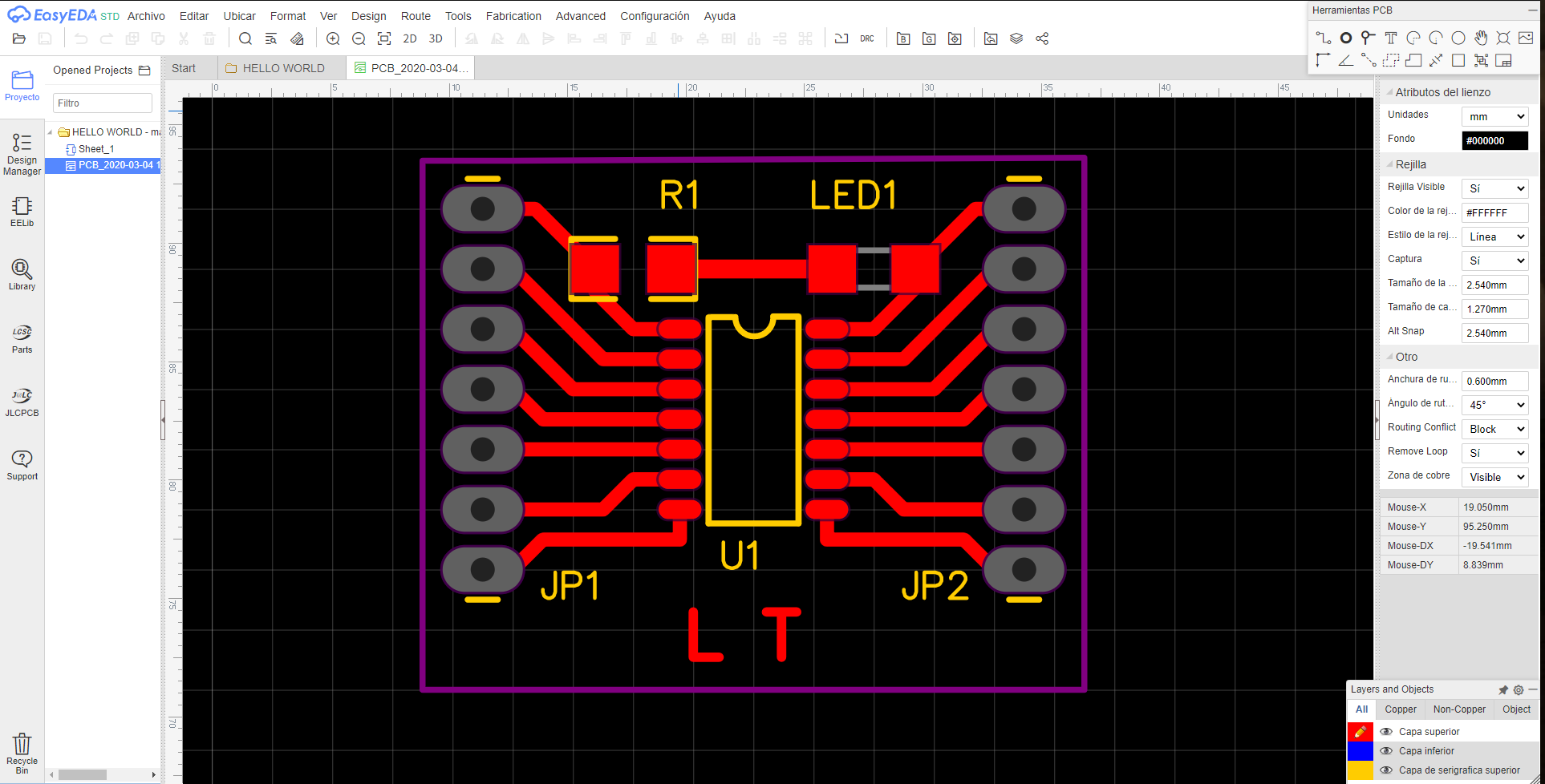 Picture 72.2.1.
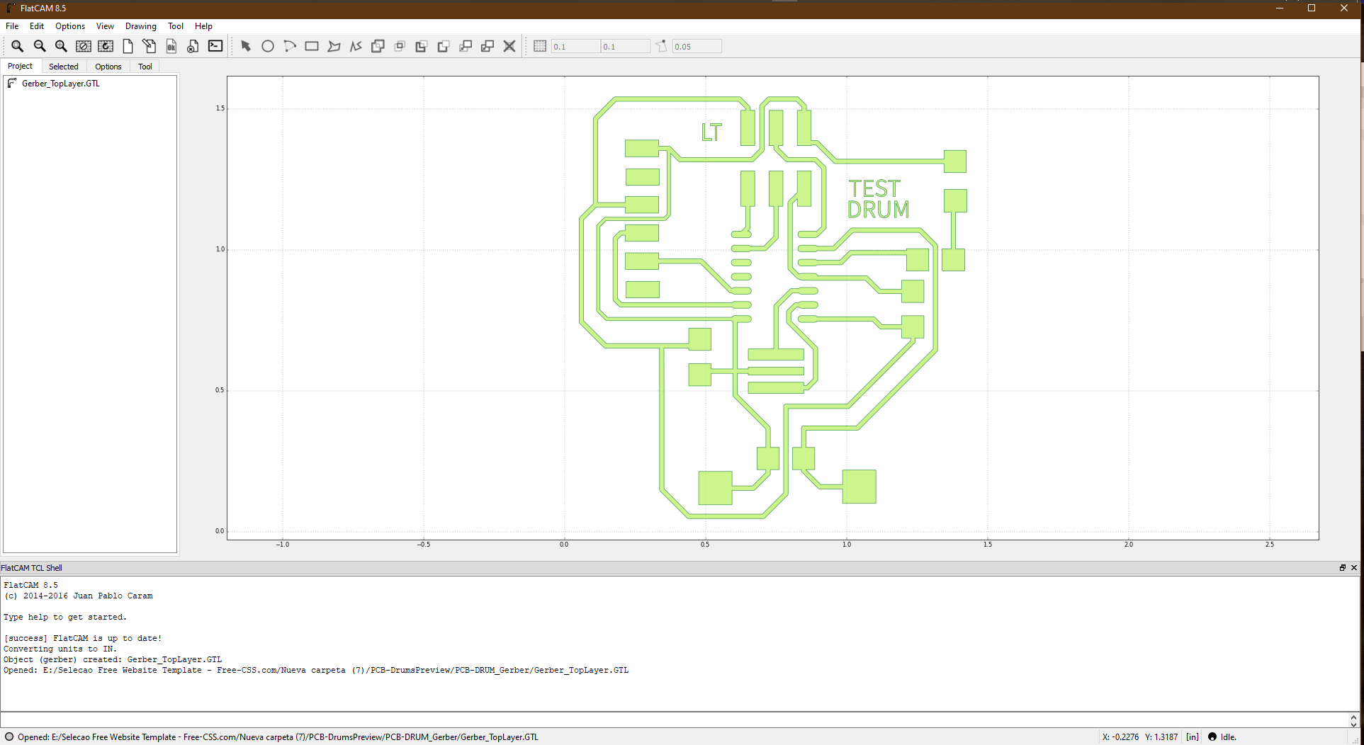
Here are the Gerber file and SVG file:
Gerber-Files
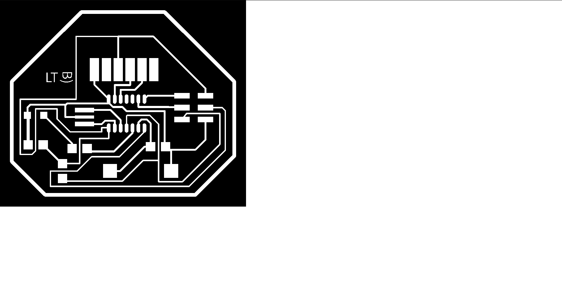
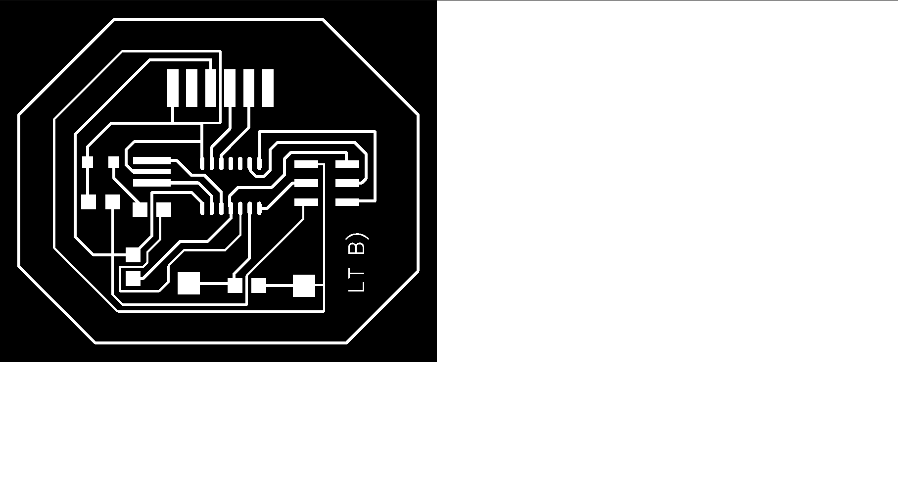
Export the EDA-document in
SVG extencion. In the picture below show a preview.
Picture 72.3. 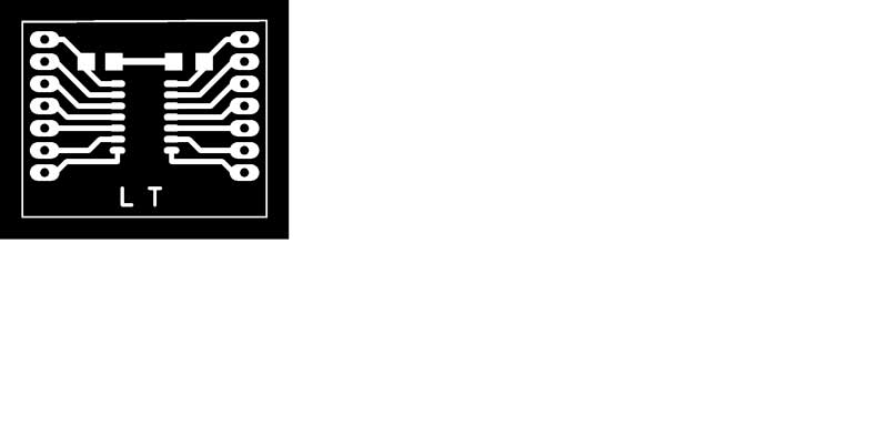 STEP 2.
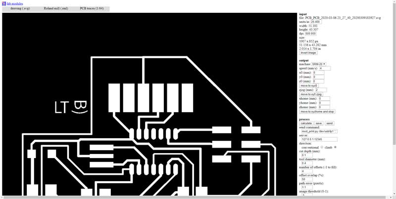
 Upload to Fabmodules. Then we use Fabmodules to prepare the schematic for the Milling machine. Here the parameters for the Milling machine, the Roland SRM-20.
Picture 72.4.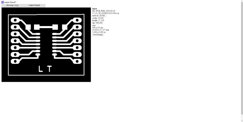 Picture 72.5.
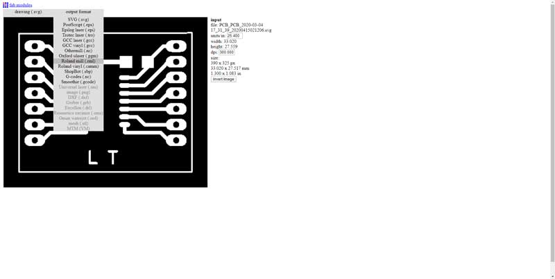 Picture 72.6.
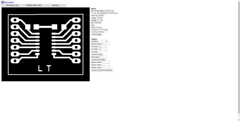 Picture 72.7.
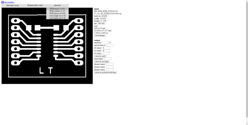 Picture 72.8.
 Picture 72.9.
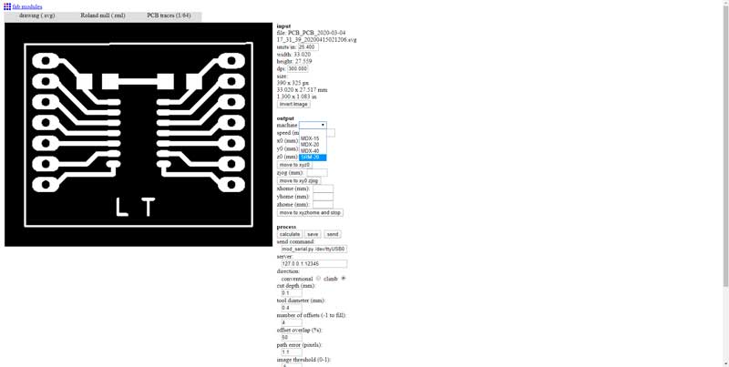 Picture 72.10.
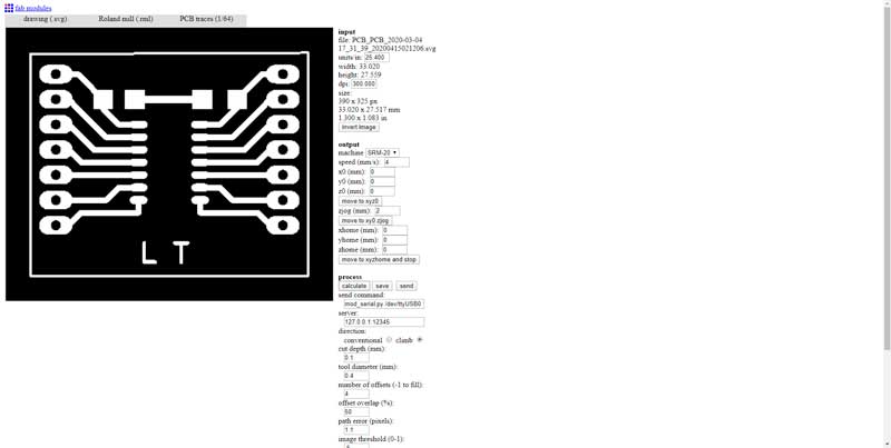 Picture 72.11.
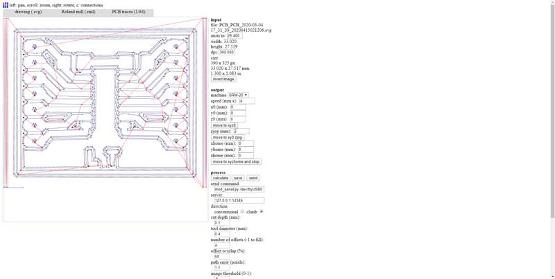 Picture 72.12.
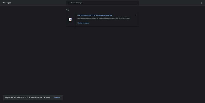
Here are the ready files to mill my PCB.
-Trace:
PCB-Trace
-Outline:
PCB-Outline
-Drill:
PCB-Drill
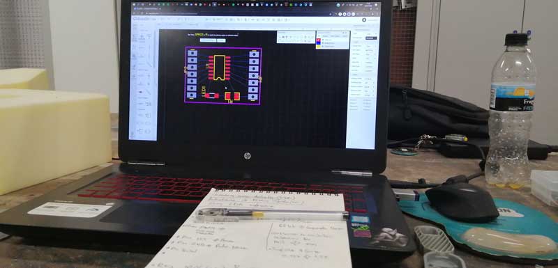
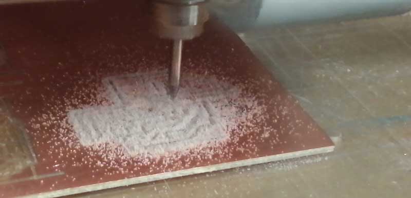
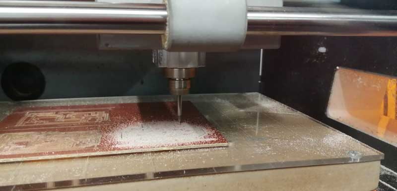
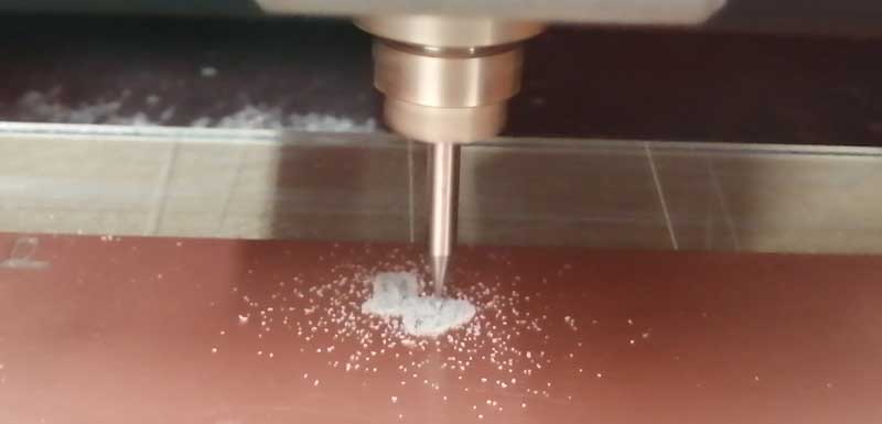
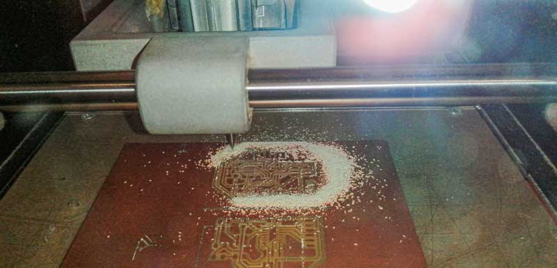
STEP 3. Milling my PCB board
Prepare de milling machine
Picture 73.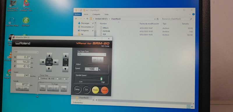 Picture 73.1.
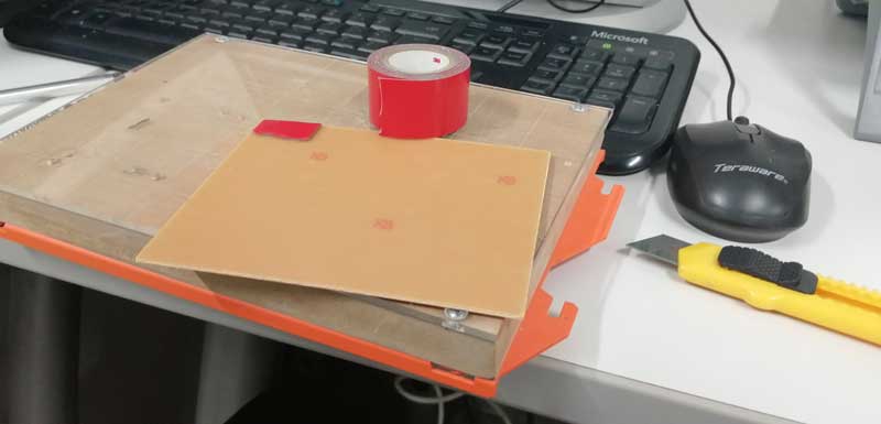 Milling the Traces
Picture 73.2.
Milling the Traces
Picture 73.2.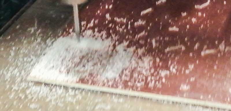 Picture 73.3.
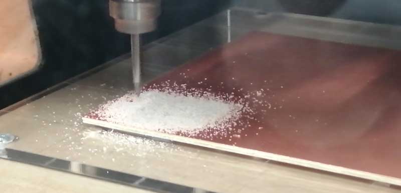 Picture 73.4.
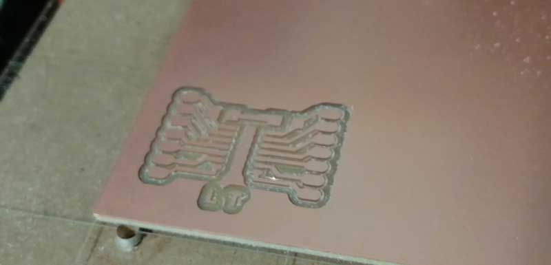 Milling the Outlines
Picture 73.5.
Milling the Outlines
Picture 73.5.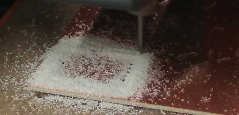 Picture 73.6.
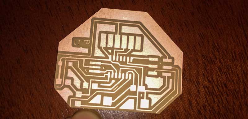
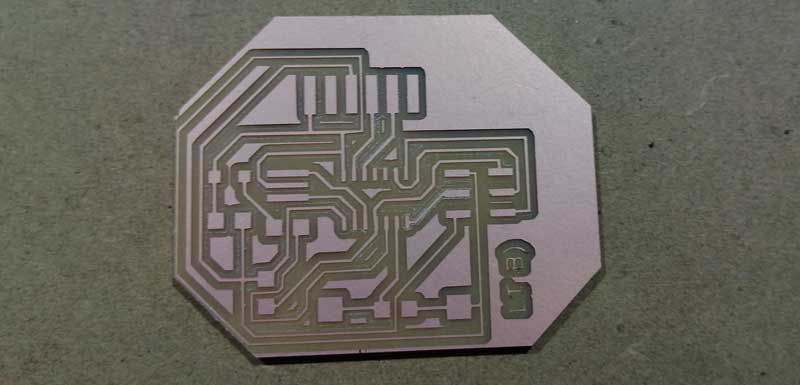
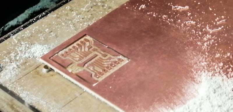 Retire the PCB
Picture 73.7.
Retire the PCB
Picture 73.7.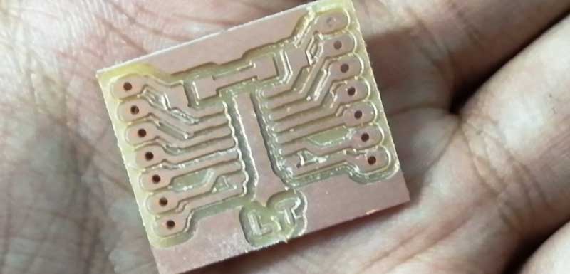 STEP 4.
 Solder the electronic components for my PCB circuit
Picture 74.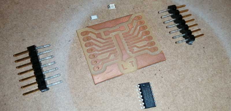 Picture 74.1.
STEP 5.
Picture 74.1.
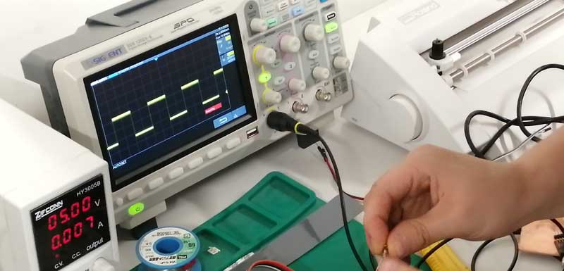
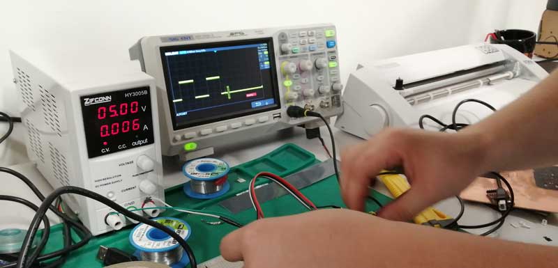
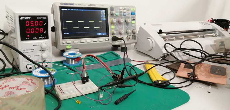
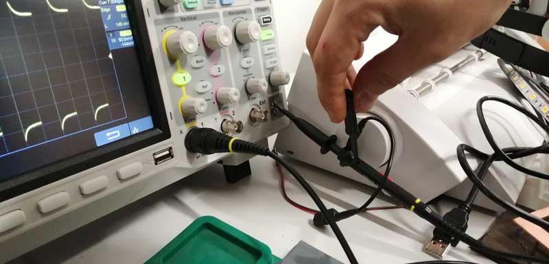
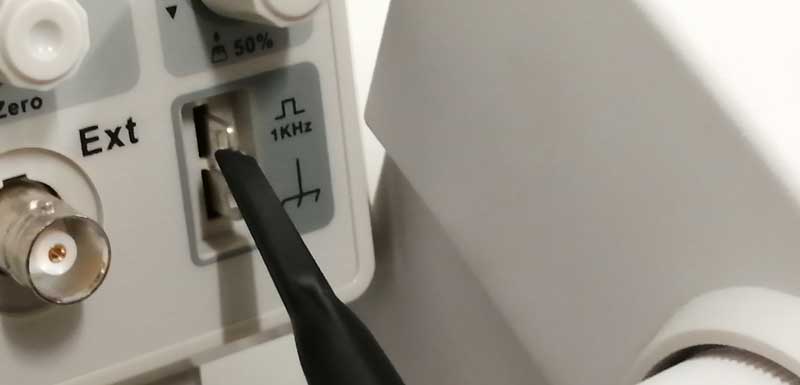
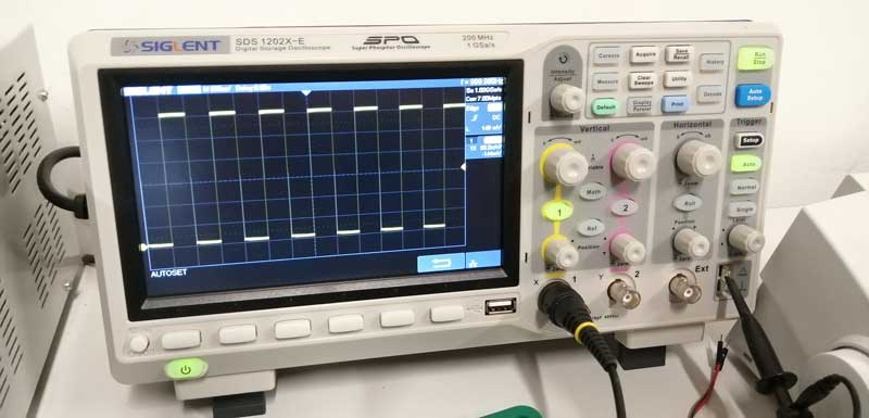
STEP 5. Programming my PCB-circuit
Picture 75.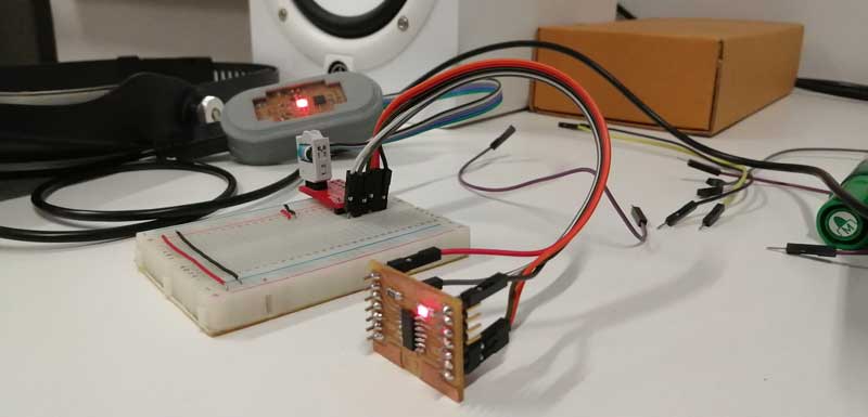


.png)
.png)
.png)
.jpg)
.jpg)
.jpg)
.jpg)
.jpg)
.jpg)
.jpg)
.jpg)
.jpg)
.jpg)