In this assignment, you design and manufacture a circuit to which you add a sensor to a microcontroller board.
== My own PCB echo hello-world ==
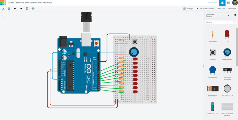
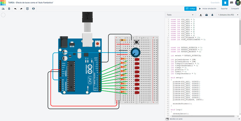
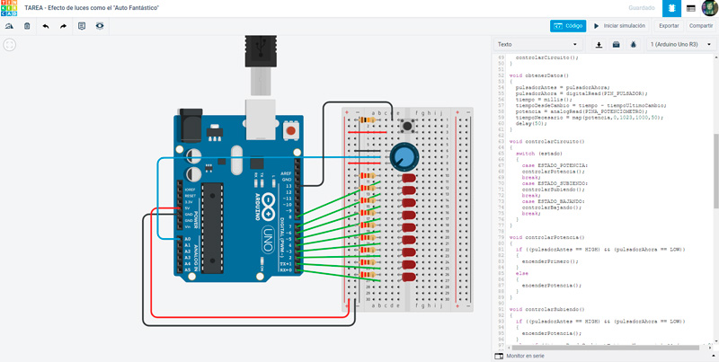
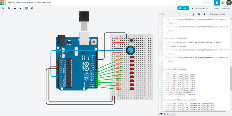
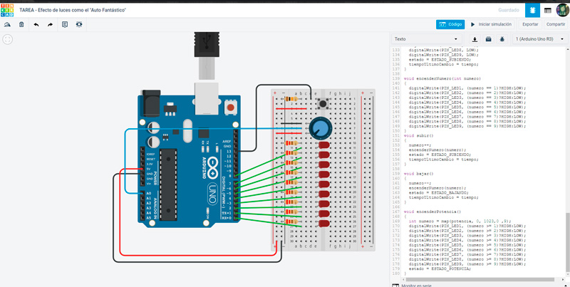
This week I worked on creating a circuit using tinkercad. I decide to use a replicate a light an LED sequence like the Khight Rider (KITT).
Below are the steps.
I share you my thinkercad file please clic on the link: Tinkercad-File
and this is the code file: Code2
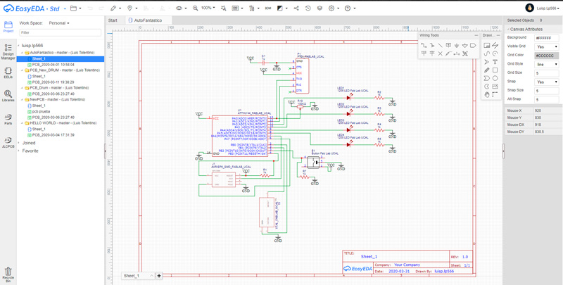
STEP 4. Use EasyEDA
After my simulation at Tinkercad, I switched my circuit to EasyEDA. At EasyEDA I prepare my circuit to be able to manufacture it on the milling machine. These are electronic components that I will use in my milled circuit:
For this circuti I used this items
ITEM
Measures
Quantities
Attiny44
-
16:00 - 20:00
Resistor 220Ohm(Ω)
-
04
Resistor 1kΩ
-
01
RED LED's
-
04
FTDI
-
01
ISP connector
-
01
Ocilador
-
01
Ponteometer
-
10k
Boton
-
01
For the PCB layout, I had two problems. First, my mind had a hard time understanding how to design and manufacture PCB cards and also know the names of each component, but now I understand and even do a few tricks. The second problem was that due to the quarantine issue, I did not manage to physically manufacture my PCB, but here I share this process that I had, I did 5 PCB circuits and also at the end I will leave the files ready to manufacture. Well I hope you enjoy it.
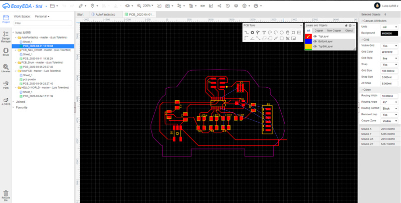
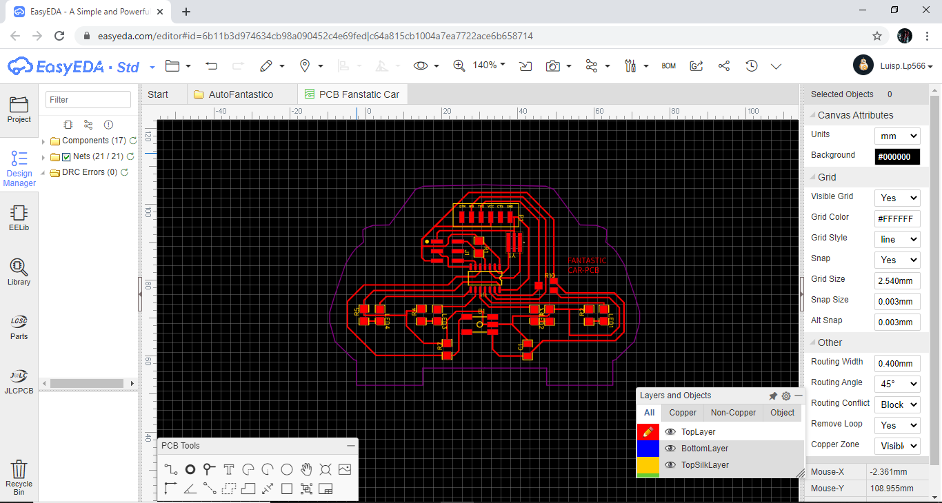
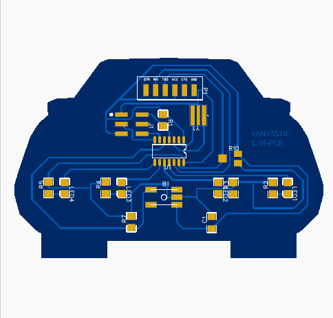
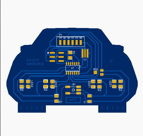
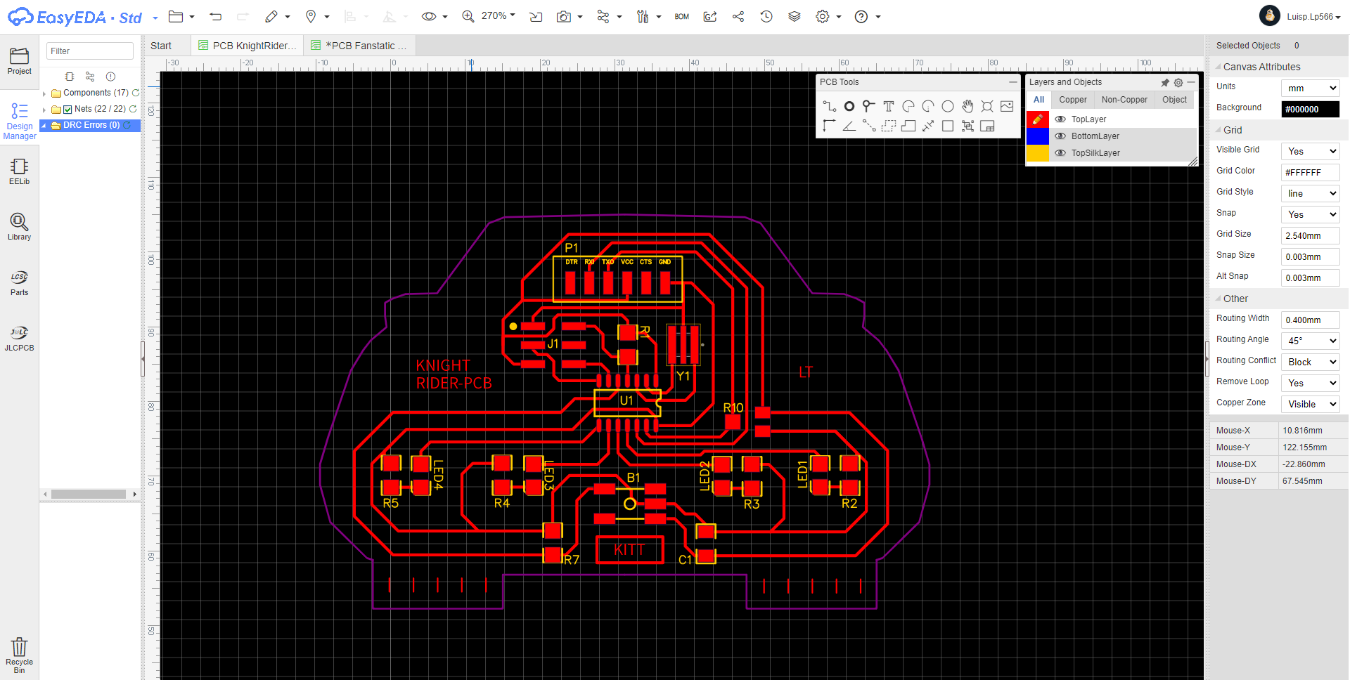
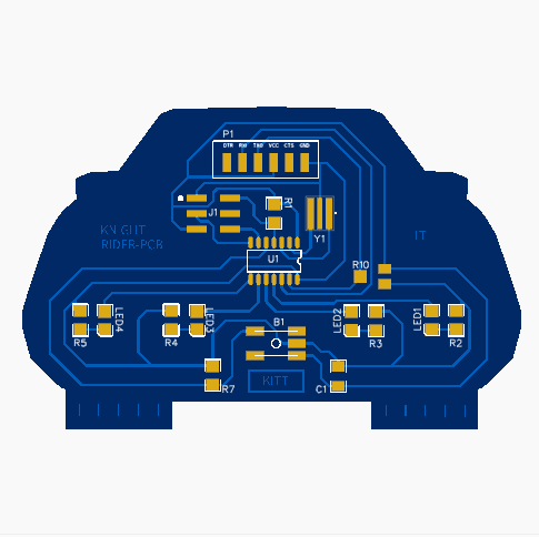
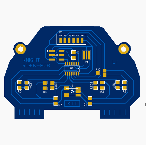
Picture 88.5.this are my squematic of my circuit of the knight rider-pcb. Picture 88.6. This was the first design of my circuit, in this part it was difficult for me since I did not know what to connect with what. and visually it's not very flashy. Picture 88.6. This was my second PCB design of the circuit. For this, I have more knowledge and I did a design visually more flashy. Picture 88.6. This was a preview of my PCB circuit in the EasyEDA viewer, ready to manufacture, but I think I can improve the layout a little more and the visual part of my circuit give the feeling that it is a car. Picture 88.6.1 This was my third circuit PCB design. In this design I improved the traces and I made a design that visually feels that you see the The Knight Rider car. Picture 88.6. This is a preview for my PCB circuit, as you can see in this preview I put some lines that simulate wheels and also I put its plate where KITT says the name of The Kniight Rider car. Picture 88.6. This was my fourth circuit PCB layout. In this design, I further improved the traces and made the components more aligned with each other is something very inperseptible but it gives a more attractive visual effect to the design. Picture 88.6. This is a preview for my PCB circuit, as you can see it is already having more visual impact. Picture 88.6. This is my final design on this PCB in this circuit I placed two holes that simulate the rear-view mirrors of the cars but as you see these holes have a purpose, I have thought of making a case in acrylic and mdf where I can display my circuit. On the other hand I put the biggest names because my name Luis Tolentino "LT" does not go well, instead of "LT" comes "IT" as the movie for this reason I decided to make the names bigger. Picture 88.6. This is the final preview for my Knight Rider PCB circuit, as you can see it is already having more visual impact and the names come out well.
I share you my EasyEDA Gerber file's please clic on the link: Gerber-File's
STEP 2. This is my milled PCB. Wait a long time to be able to manufacture and solder it. But I managed to do it.
In my final project the input device part this is what I did. I show you some images, but I leave this link for you to see more about the process of the project. Final Project.
-------. DESIGN THE PCB .-------
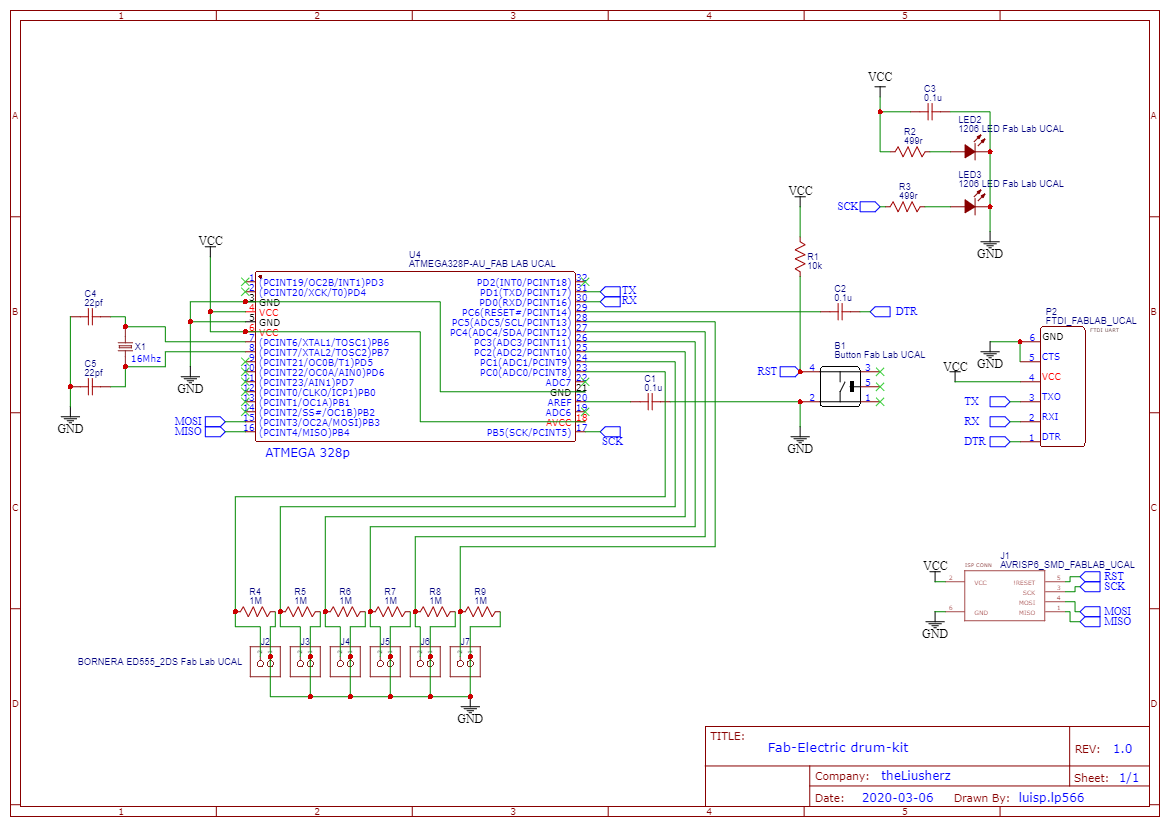
In EasyEDA I draw my schematic and trace my PCB circuit.
Picture DMS2.0. Here are my file of my schematic: Download.
Once I have finished making my schematic, I step to draw and trace my pcb.
Picture DMS2.1. This step was very difficult, because I had to think a lot and it was difficult to connect all the components correctly tracing the entire PCB in addition to creating a layout for my PCB.
Picture DMS2.2. This are the preview view of this PCB. This is the PCB that I mill and use on my drum.
Export Gerber and open in FlatCAM
Once the trace of my PCB is finished, I export the Gerber files from EasyEDA. To later open them in FlatCAM, prepare my PCB for milling.
Picture DMS2.3. In the picture below I show my traced open in FlatCAM.
Picture DMS3.0. I open the roland mill software and configure it to mill the trace from my PCB.
Video FV2.0. First I mill the trace and used a endmill 1/64".
Video FV2.1. Second I mill the holes.
Video FV2.2. Third I mill the outline.
Picture DMS3.8. Once the milling is finished, I clean it with the brush.
Picture DMS3.9. With the help of a scalpel, clean some residues in the traces.
Picture DMS3.10. This are the final view of my PCB.
-Electronics Componets I need to used on my PCB Circuit-
Picture DMS1.0. In the picture below I search the componets I need to used in my PCB.
Picture DMS1.1. This are the componets I need to soldering into my PCB.
-------. SOLDERING THE PCB .-------
Picture DMS4.0. The first componet to I solding is the Atmega328.
Picture DMS4.1.
Picture DMS4.2. Next I solding the other componets.
Picture DMS4.6. This is the top of my PCB.
Picture DMS4.7. This is the back of my PCB.
Debbuggin the PCB
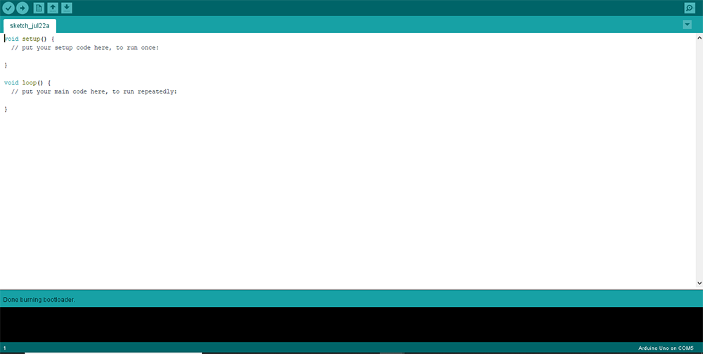
For this I burn bootloader code on the DRUM PCB.
Screenshot 1. Everything's alright. YEAH!
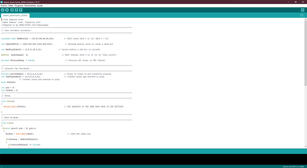
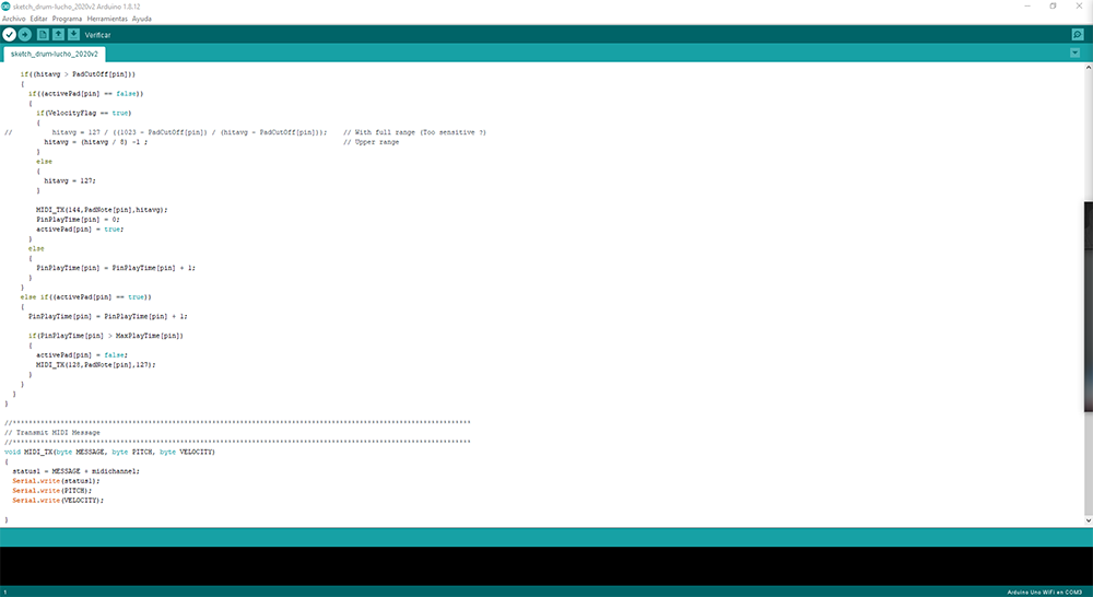
-------. PROGRAMING THE PCB Drum .-------
I am going to test the Piezo as an input.
Testing the Piezo, when I hit the piezo turn on a red LED.
Picture EC1.0. In the image below I show my soldered PCB ready to program and upload the drum code.
Picture EC1.1. I first feed my PCB via my Programmer and upload a blink to my PCB using the Arduino IDE.
Video FV3.2. It's works the Blink!.
Video FV3.2. In the video below I show the Piezo - PCB communication_TEST1
Video FV3.3. In the video below I show the Piezo - PCB communication_TEST2
Picture P1.0. I upload to my PCB and incidentally I will test the communication with the respective software.
========== learned/conclusions ==========
Aqui pude poner en practica lo aprendido en asigment anteriores. Aqui reforce mas el tema de soldado y trasado de PCB's.
Group-Task
====== Osciloscop =====
Group assignment: Probe an input device’s analog levels and digital signals.
I use a led as output to find the reading voltage per time in an oscilloscope. Notice the simple code in Arduino.
I use a delay of 30 ms for turning on with a delay of 50 ms to turn off the led. After for comparison i change the delay in both cases for the same amount, 50 ms. It is quiete impossible to notice by our eyes but the oscilloscope detect it. Notice that the line below is larger than that at the top.


 Picture 88.6.1
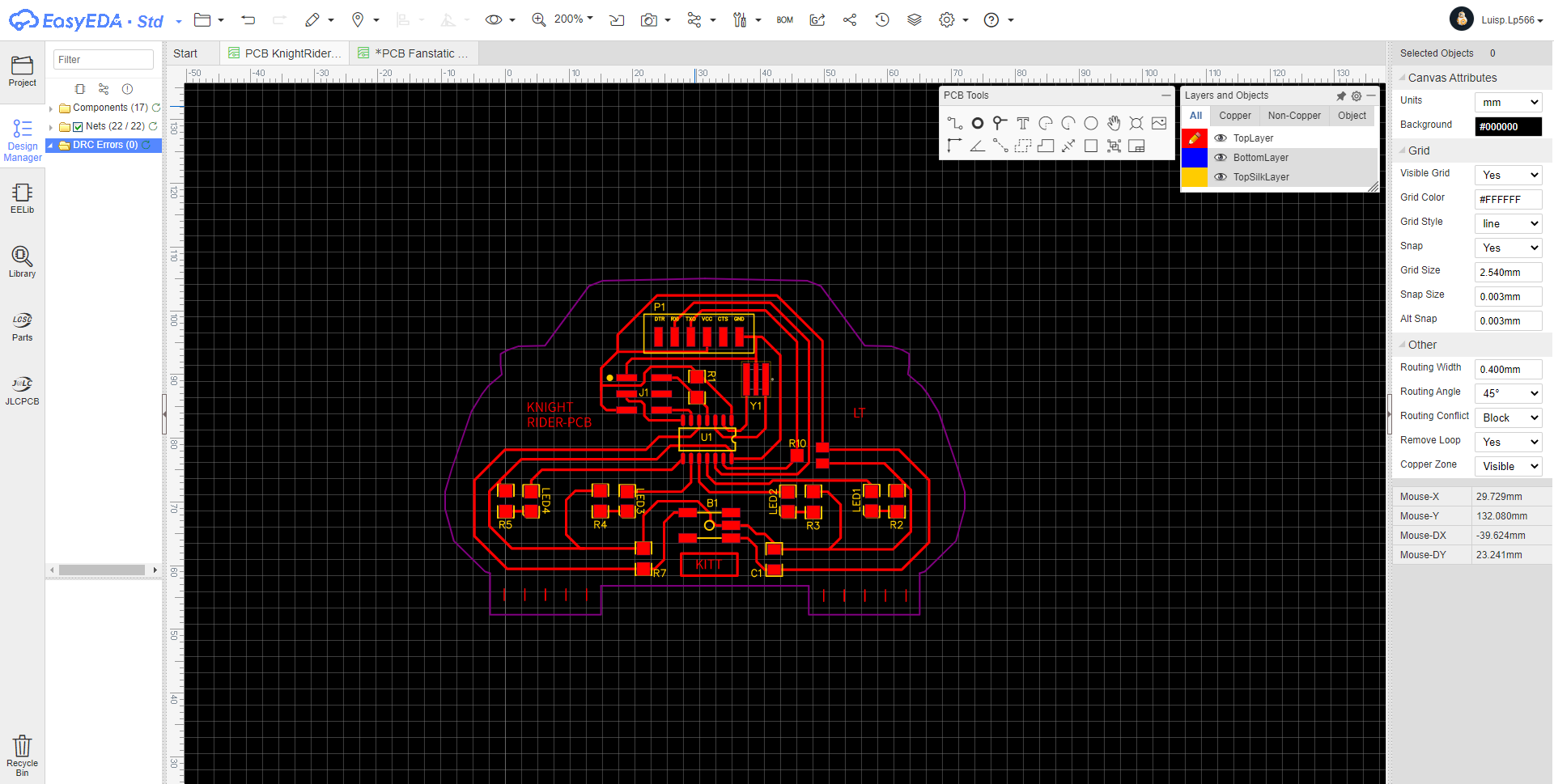

.jpg)
.jpg)
.jpg)
.PNG)
.PNG)
.PNG)
.PNG)
.PNG)
.PNG)
.jpg)
.jpg)
.jpg)
.jpg)
.jpg)
.jpg)
.jpg)
.jpg)
.jpg)
.jpg)
.jpg)
.jpg)
.jpg)