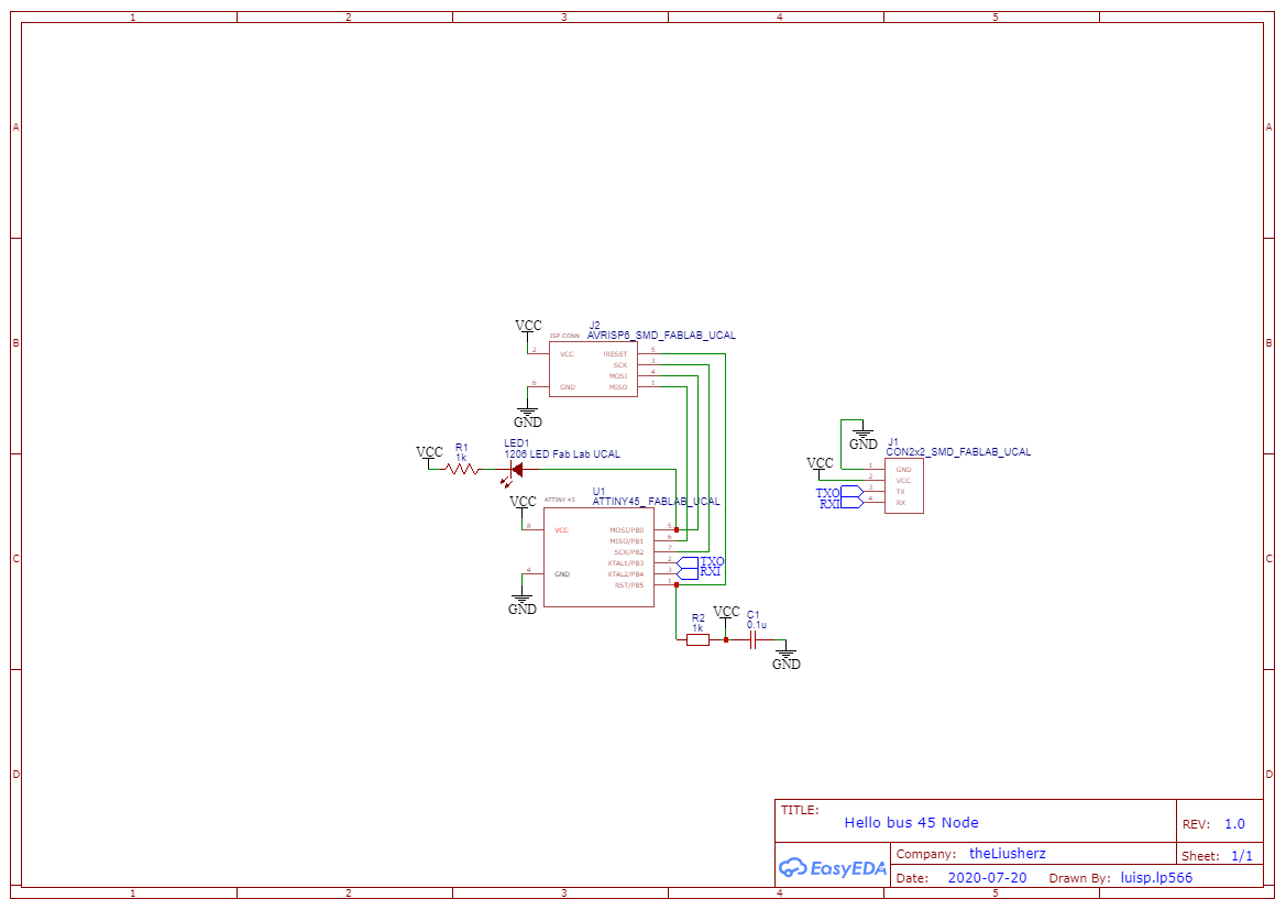
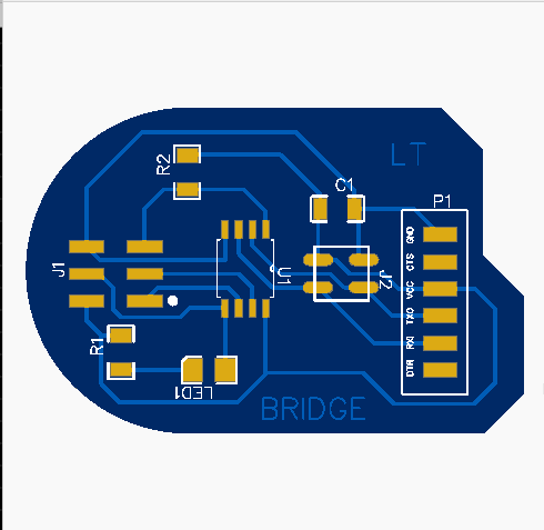
For this assigmetn I decide to designed two PCB's based on the hellow bus 45.
Picture 92.1. BrigePCB
 Picture 92.1.
 NodePCB
One PCB is the Bridge PCB and the other PCB is the Node PCB. For do this I used
EasyEDA for do mi design, For me is a simple sofware and are simple to use. Below are the steps.
STEP 1. Design and drawing in
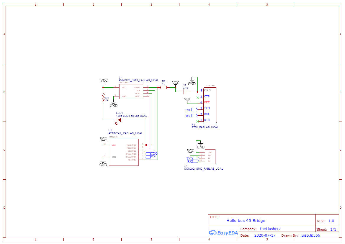
EasyEDA First I write my Schematic of both PCB's.
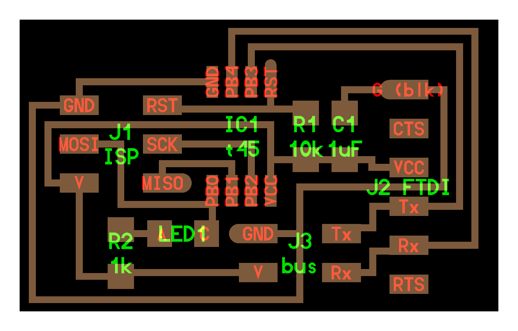
BridgePCB
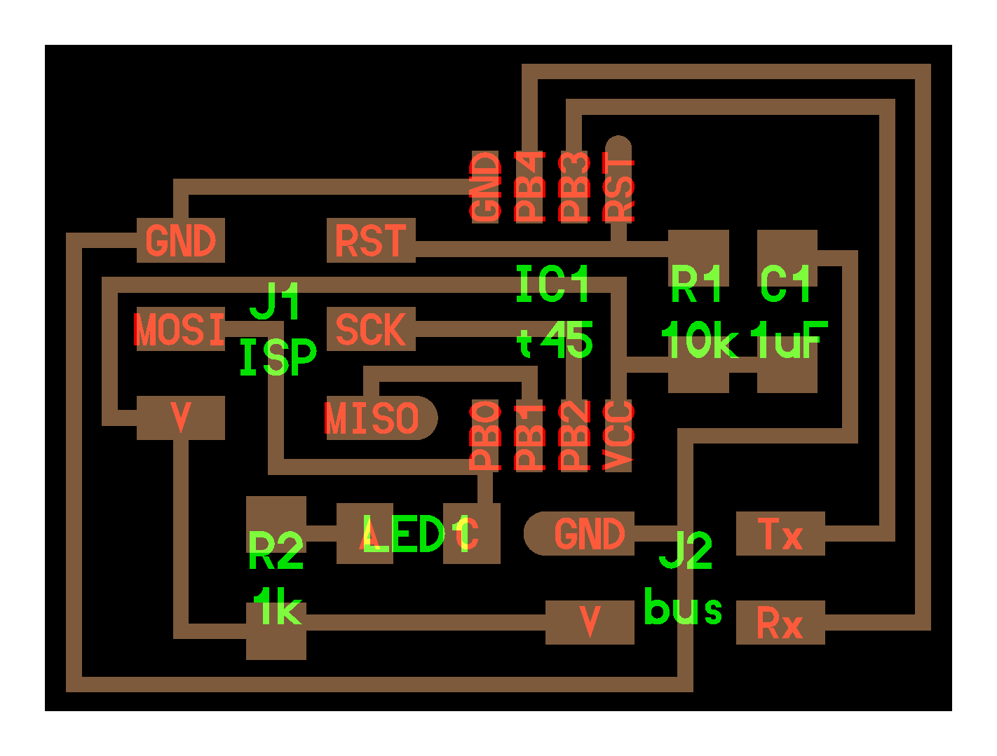
 NodePCB
 Picture 92.1.
.png)
 Picture 92.1.
.png)
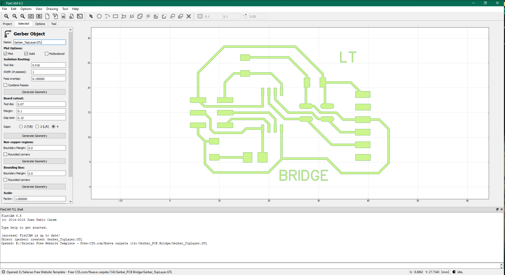
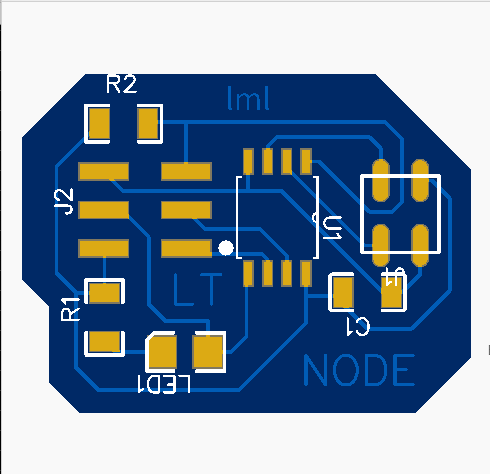 STEP 2.
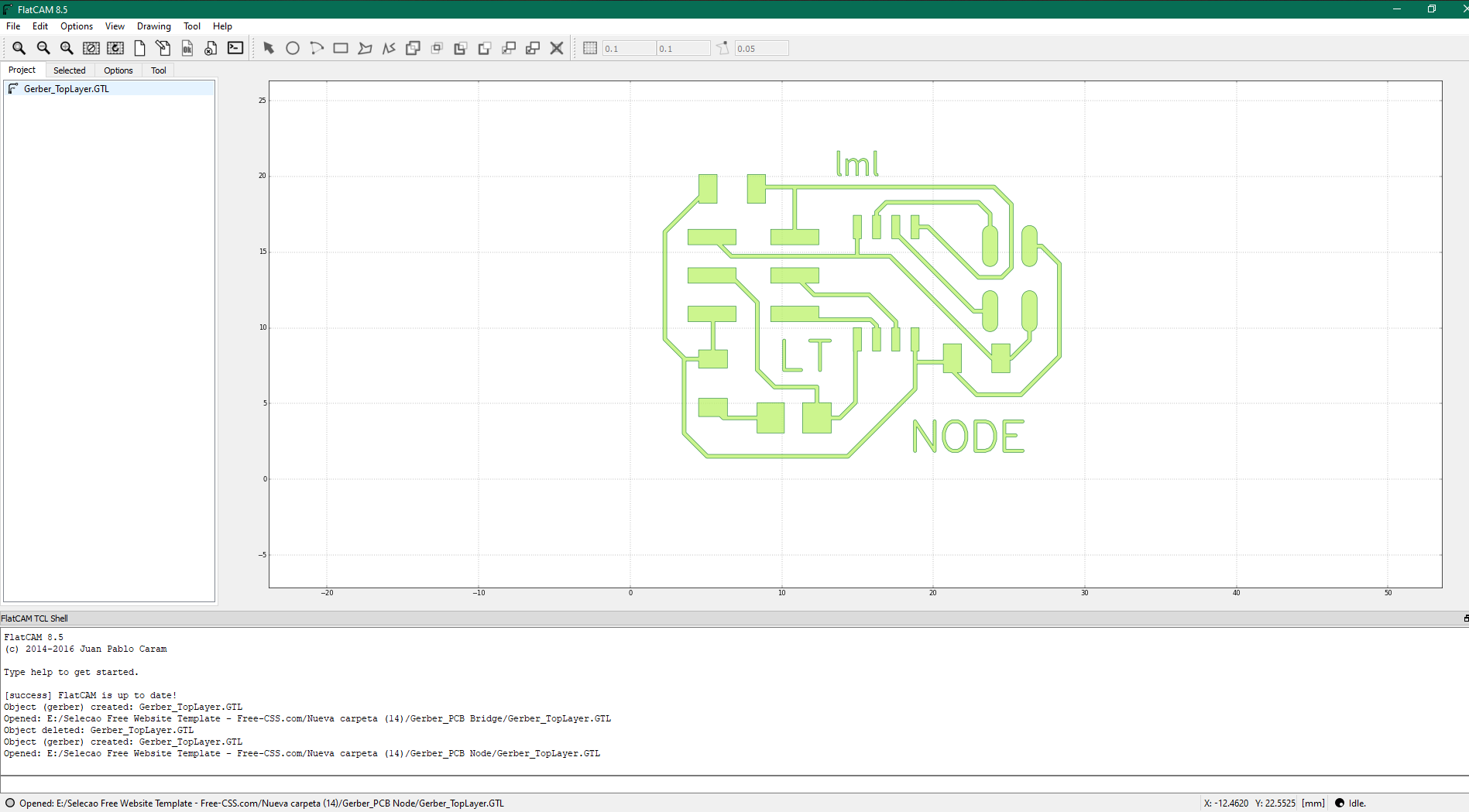
 I open the gerbers files on FlatCam and prepare to milling.
Picture 92.1. In the image below I show my
PCB Bridge in
FlatCam where I will prepare the file for milling.
 Picture 92.1.
 In the image below I show my
PCB Node in
FlatCam where I will prepare the file for milling.
 STEP 3.
 I Programing on Arduino.
When i tried to make the bridge and node to work, something wrong appeared, and it was that the reading lecture isn’t related to the number but appeared diffent codes. I double checked the schematic with my pcbs and everything appeard to be ok and after checking possible mistakes and different works done before, i review the code posted in the FabAcademy Class and i change the delay that was origally setup for 100 to 102 and it does work.
Link to the C Code
that can be copied to Arduino.
I do change “node id” in each programming.
Picture 92.2..jpg)
And i change the delay to 102 first and then to 104 and now my networking connection worked as expected. Take in account this change to let the program communicate and receive the signal.
Picture 92.2.1..jpg)
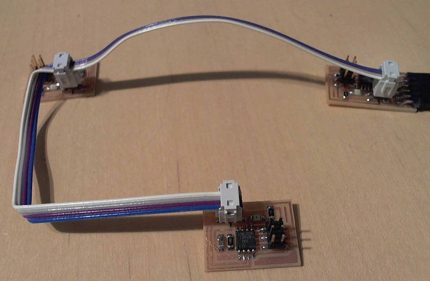
The final PCBs before i start the communication using a FTDI cable.
Picture 92.2.2.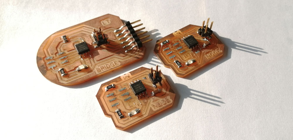 STEP 6.
View final
Finally the networking task done where the Node 0, node 1 and node 2 blinks.
Picture 93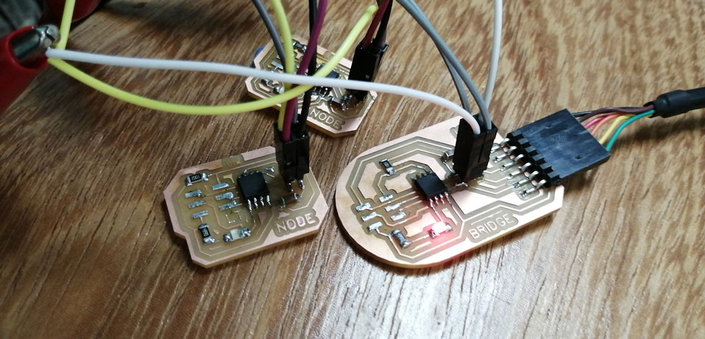 Video01.
Networking - Bridge - Two Nodes
Group-Task
1.Send messages between two projects.
Partner’s Group Link - Manuel Corrales Arana
After connecting both assingments, my partners and mine, we reached the communication between both. My partners Nodes are: 1, 2, and 3 My Nodes are called 4, 5, and 6
Picture 25.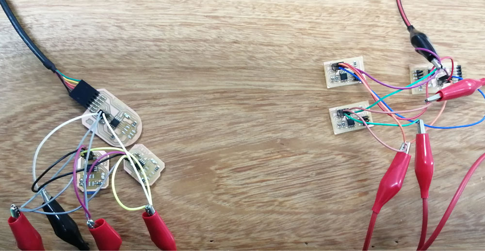
Here the video of how both projects communicates.
Video01.
Interesting assignment that allows me to think about how devices talk each other.
========== learned/conclusions ==========
In this assignment I enjoyed giving a unique design to my pcbs and watching them mill. But both Manuel and I have problems in the programming part. Try after try we achieved nothing. but in that we realized an error in the code and we corrected it and it still worked.
It was interesting to see how with a simple command the six connected pcbs communicated with each other.
=============== FILES ===============