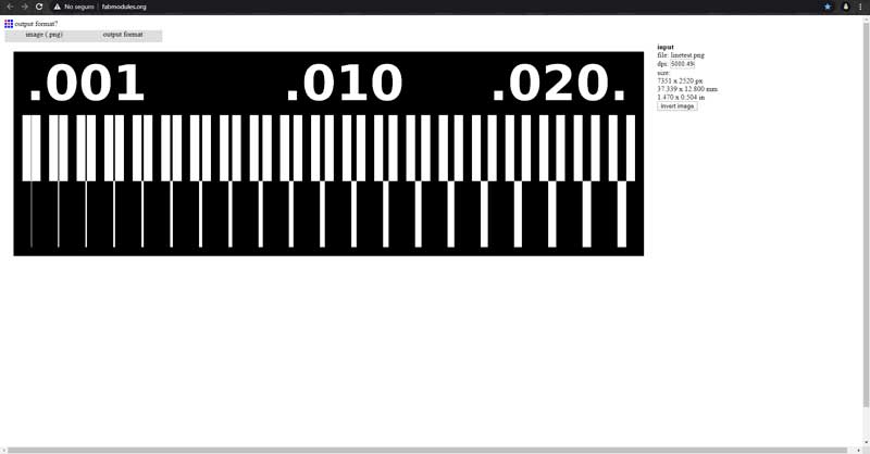
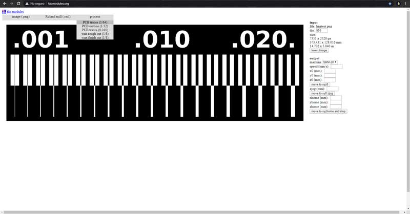
For this assigment I worked with
Roland SRM-20 and use
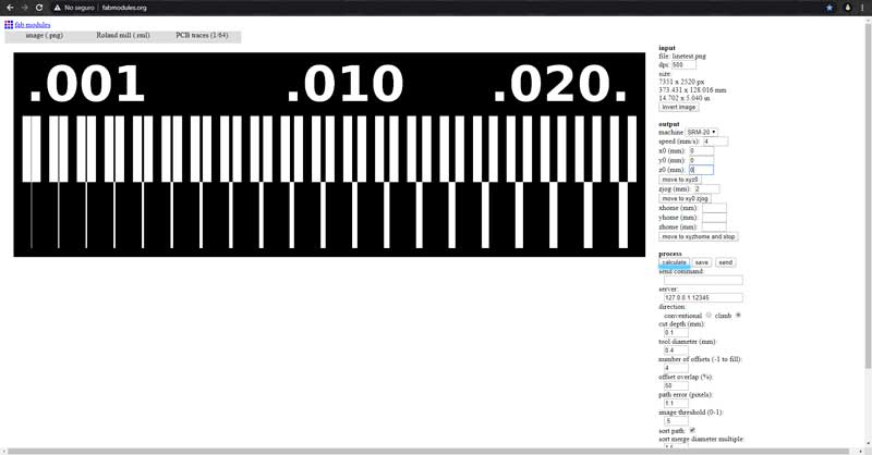
FR1 (phenolic paper) material for made this assigment I use two endmill
1/64 and 1/32.
Picture Endmill.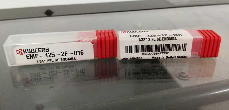
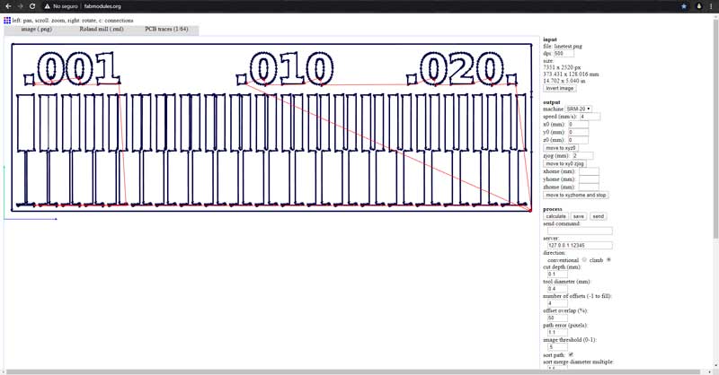
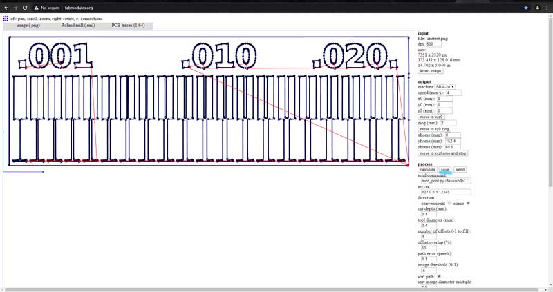
I show the
process as shown below step by step.
STEP 0.
In the following images I show my first practices and learning welding electronic componets and some welding techniques.
But this is clear, to learn to weld is practical and practical, the easiest components are the resistors, LEDs, capacitors and crystals. The ones that were difficult for me but in the end I learned to solder were the microcontrollers, buttons and RGB LEDs.
Picture 46. 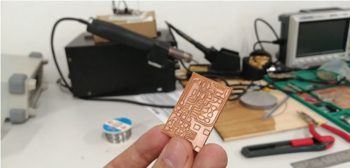 Picture 46.1.
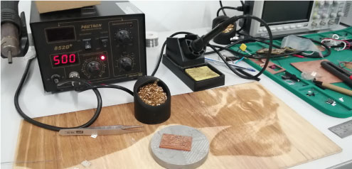 Picture 46.2.
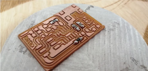 STEP 1.
 My instructors and my partner and me we create our own
FablabUcal PCB-In-circuit programmer in
EasyEDA.Std
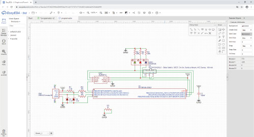
Picture 47. This is the schematic of the Ucal-Programer.
 Picture 47.1.
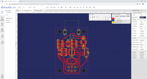
 This is the final design of the Ucal-PCB-In-circuit Programer.
Then we upload the exported files from
easyEDAb> to the
Flatcam software. For this part, my instructors did the setup to speed up the job as they wanted us to practice more on
welding electronic components and how to use the milling machine.
Picture ex1.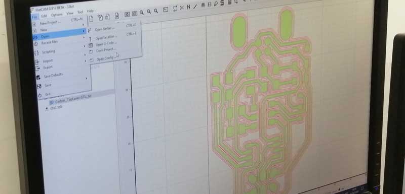 Picture ex2.
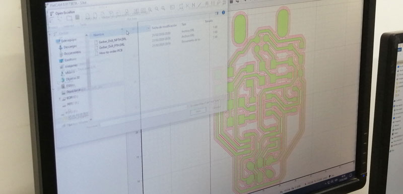 STEP 2.
 Prepared the Roland SRM-20 charge the PCB paper.
Picture 48.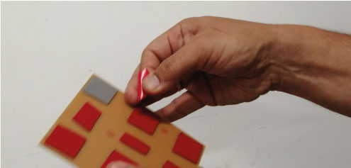 Picture 48.1.
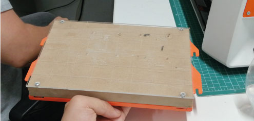 Picture 48.2.
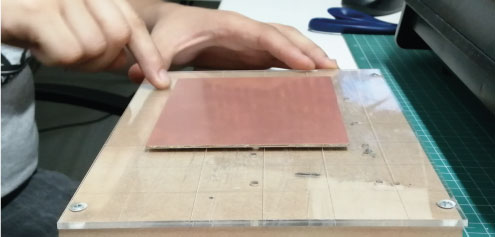 Picture 48.3.
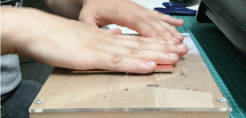 Picture 48.4.
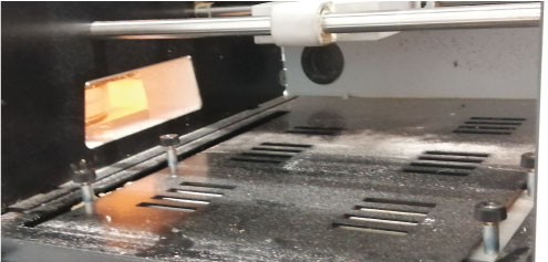 Picture 48.5.
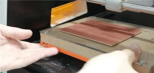 Picture 48.6.
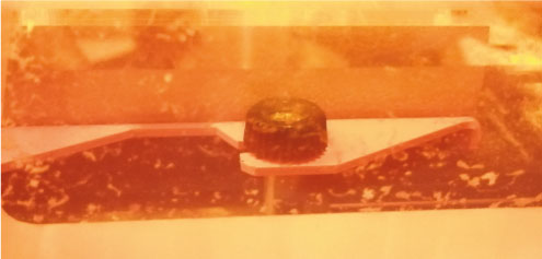 Picture 48.7.
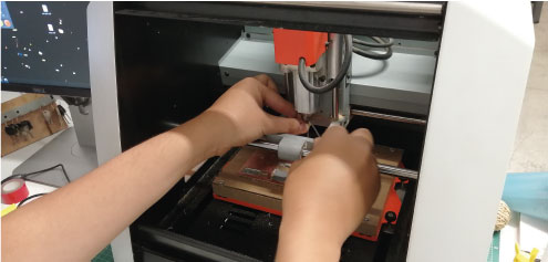 STEP 3.
 Prepared the Roland SRM-20 to milling.
Picture 49.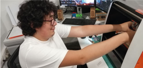 STEP 4.
 Prepared the Roland SRM-20 to cut.
Picture 50.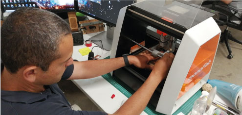 STEP 5.
 I removed the milling PCB from the milling machine and I selected the electronic components before welding
Picture 50.1.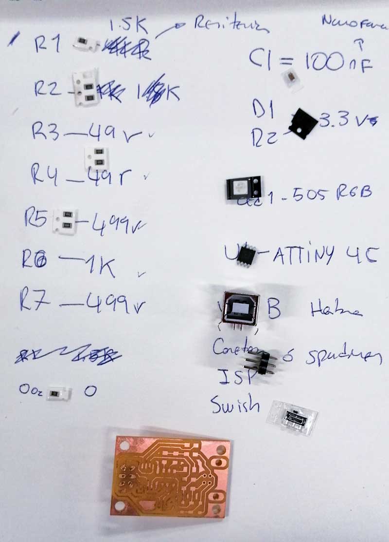 STEP 6.
 Welding
Picture 51.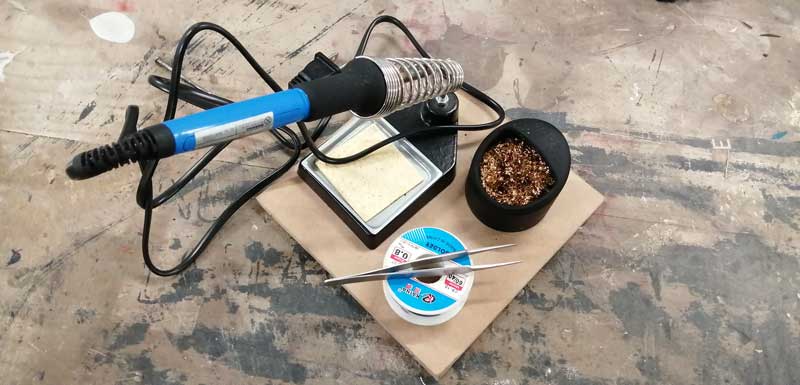 Picture 51.1.
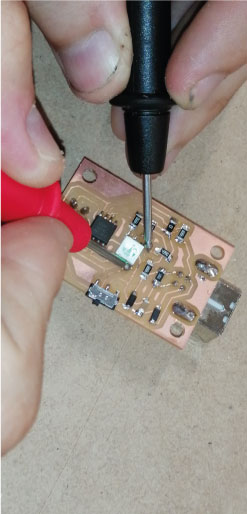 STEP 7.
 View final
Picture 52.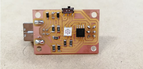 Picture 52.1.
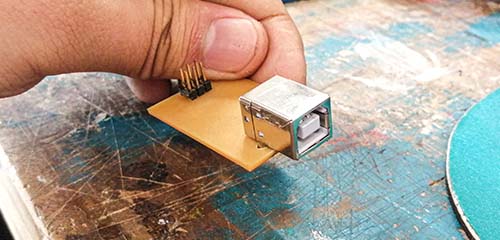 Picture 52.2.
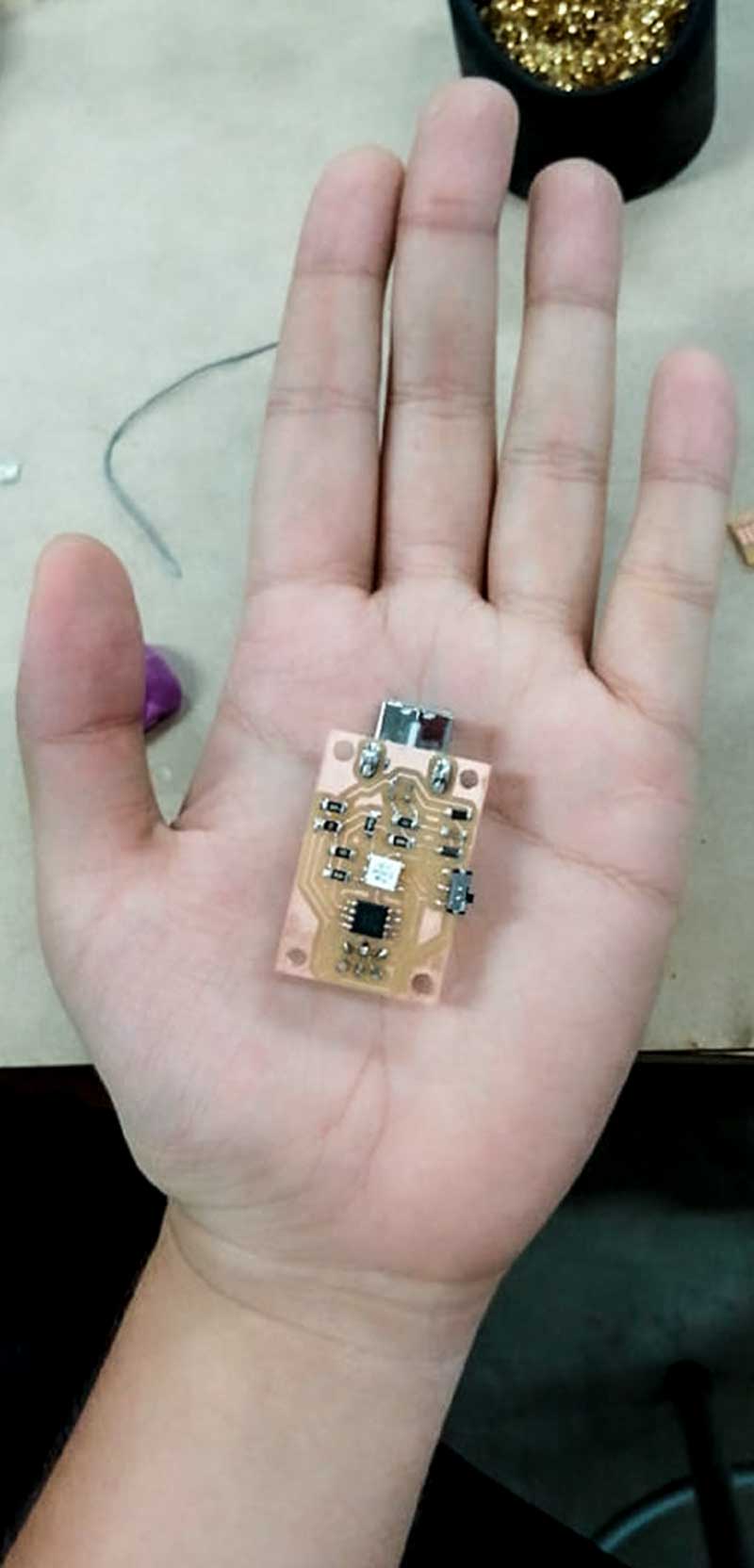 STEP 8.
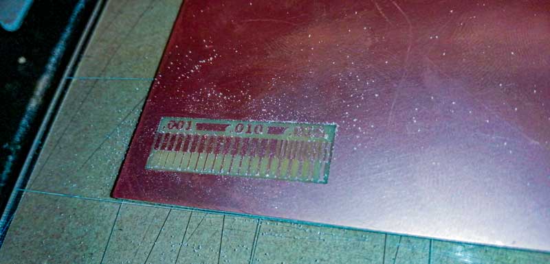
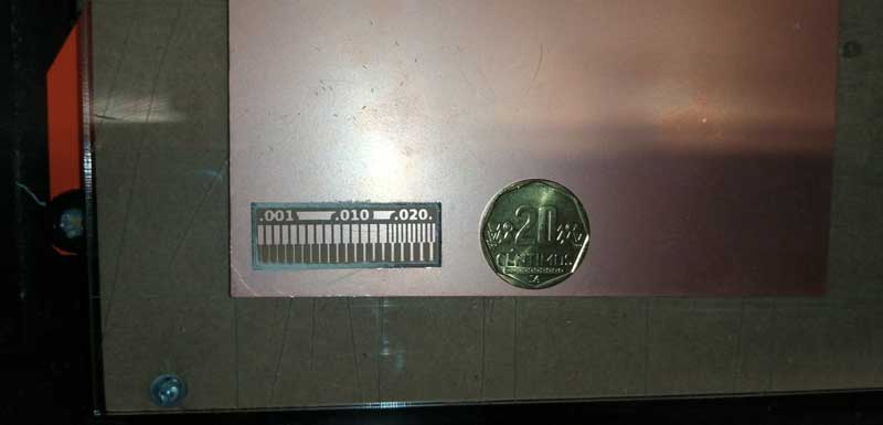
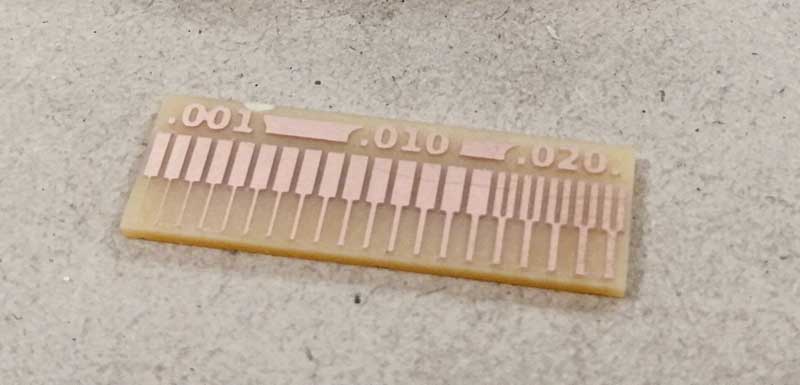
 Manufacture the Ribbon Cabe.
Picture 53.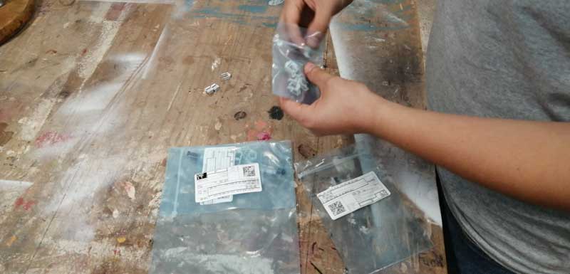 Picture 53.1.
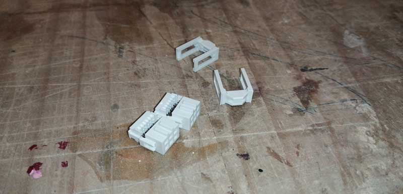 Picture 53.2.
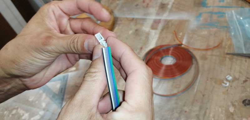 Picture 53.3.
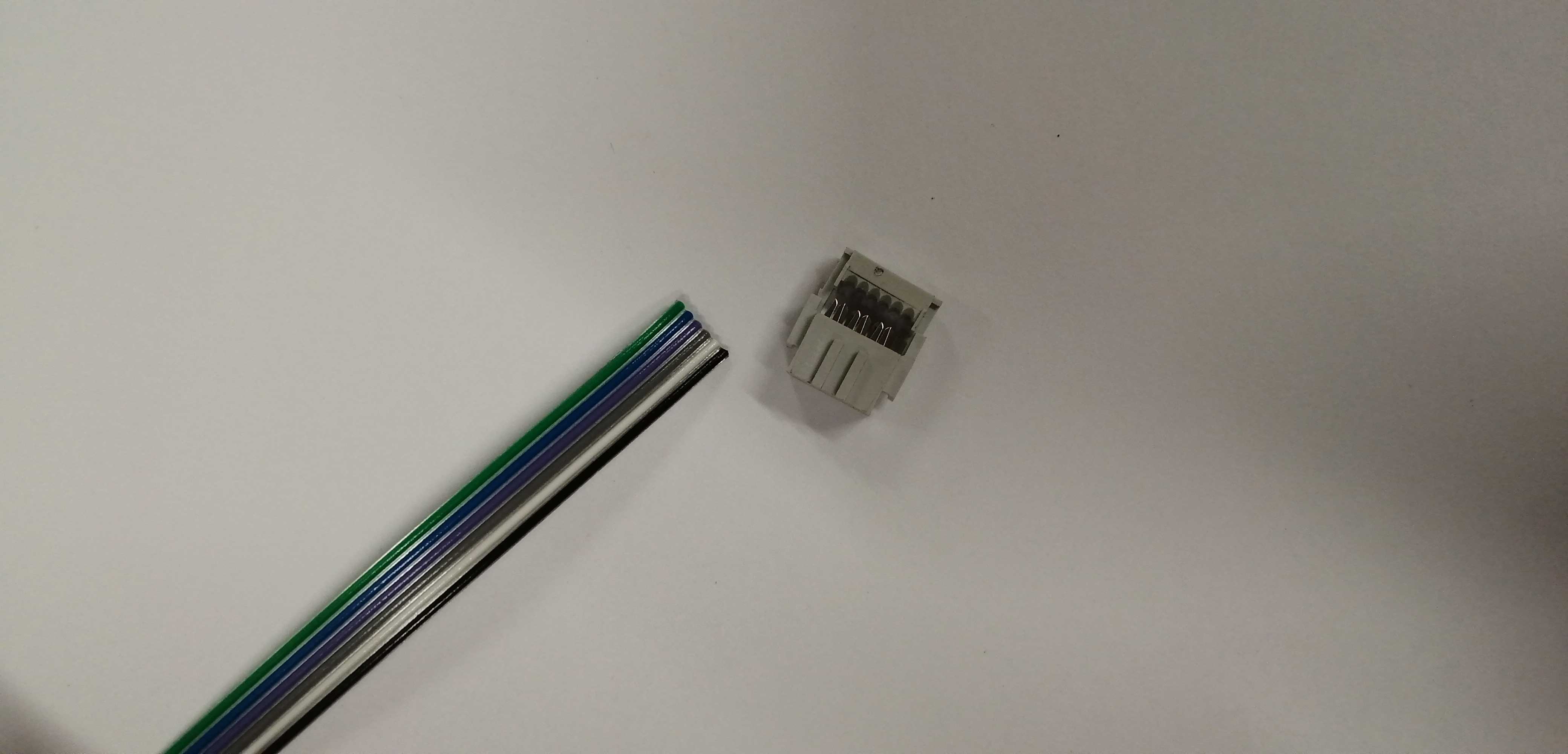 Picture 53.4.
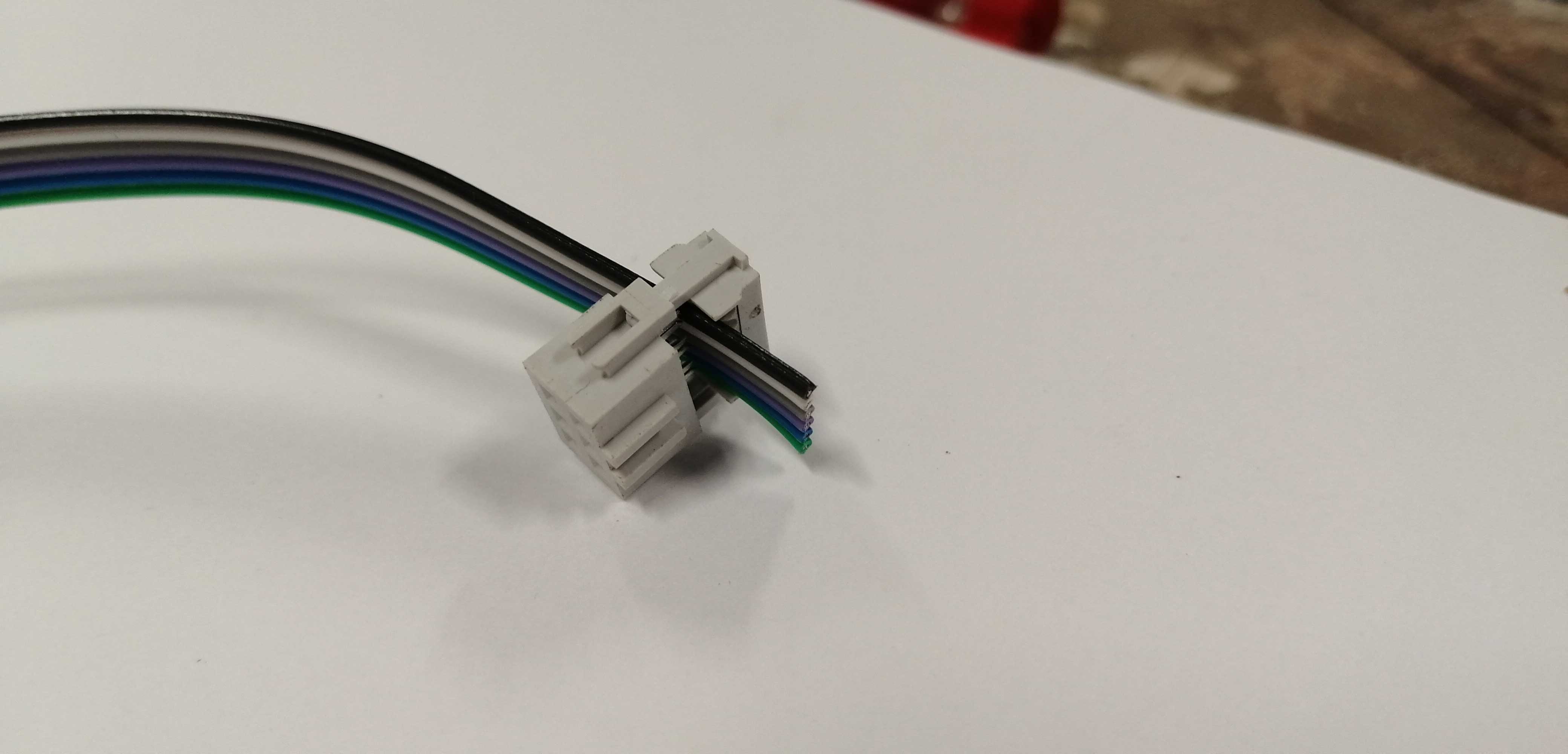 Picture 53.5.
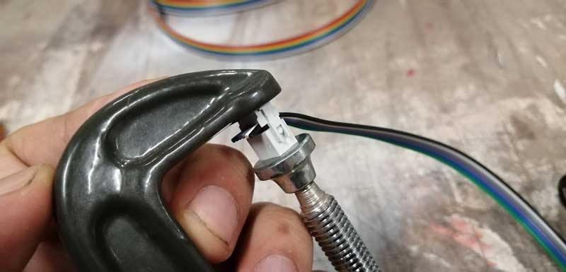 Picture 53.6.
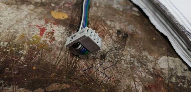 STEP 9.
 Programming
This was the most difficult part because we
(my partner and my) write new tipe of code. Therefore we read the indications that are in the schedule but in a hurry forget write one step in the programing
(5.make rstdisbl), this setback delayed our work for
three days, as we believed that our cards were
badly soldered, we also believed that they
had a short circuit to guarantee that they worked well we decided to re-manufacture everything from scratch, it was very stressful and frustrating that our work didn't work, but we dided.
Picture PCB'srUsing the Multimeter to check if it does not have any short circuit
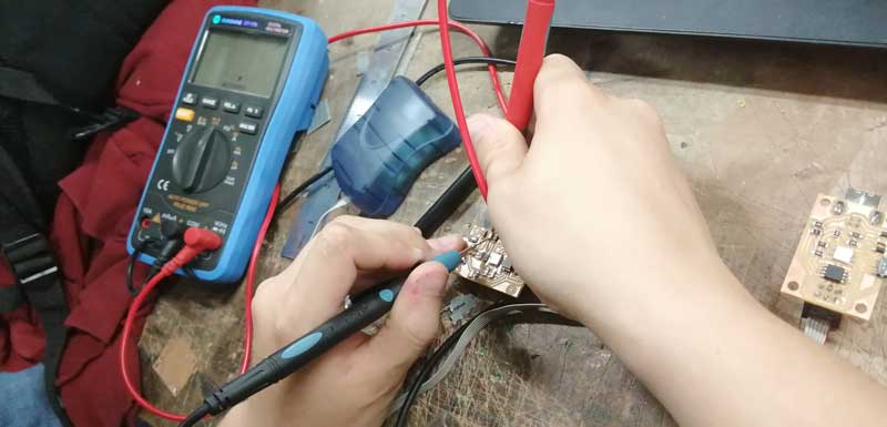 Picture PCB's 1
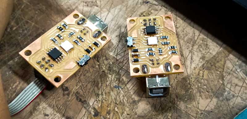
After several tries, we re-read and went through programming step 5 when we realized this, we laughed and thought, saying that we had to read the instructions well and patiently.
Then we rewrite all the programming steps correctly until it worked properly by turning on the RGB light of the programmer.
We use
3 LEDs colors: 1.Purple = Programming --2.Green = no power (needs external power) -- 3.Red = power.
Programing Steps:
1.cd
Picture 54.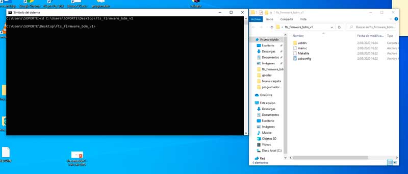
2.make
Picture 54.1.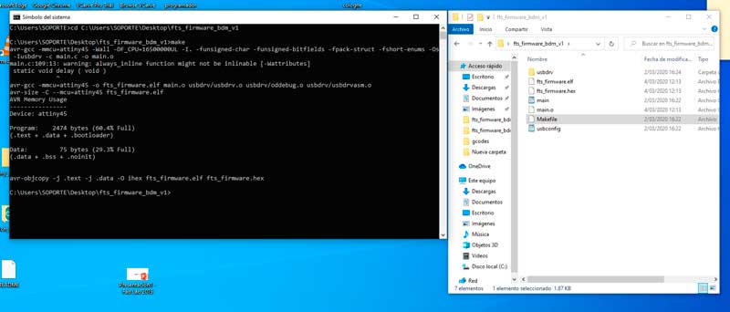
3.make flash
Picture 54.2.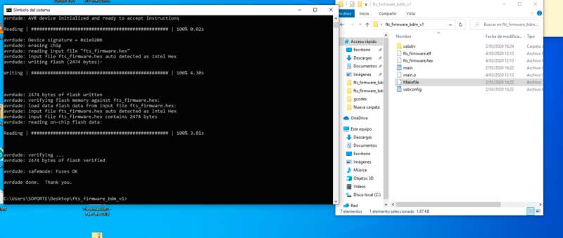
4.make fuse
Picture 54.3.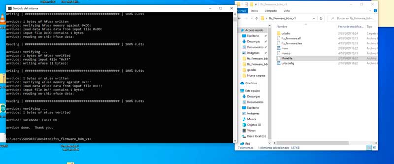
5.make rstdisbl
Picture 54.4.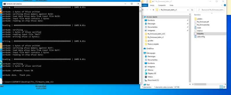
Video
Video Programing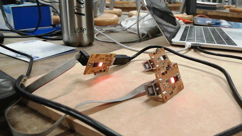
.