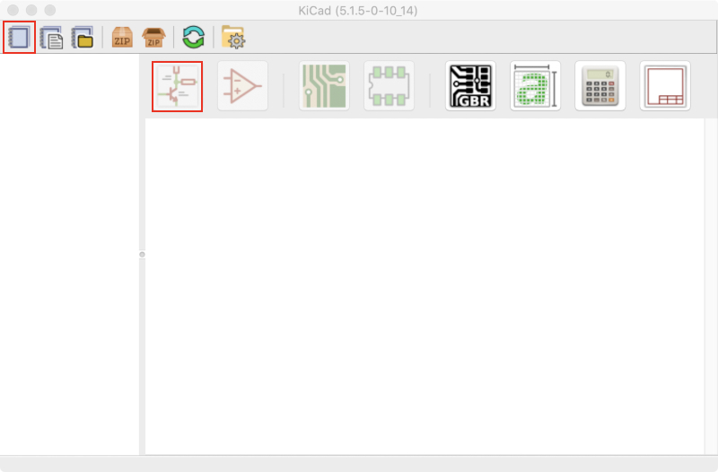
Kicad
Workflow
- Downloaded Kicad.
- Opened Kicad and created new project named 'Kicad demo'. And Opened Schematic Layout Editor.
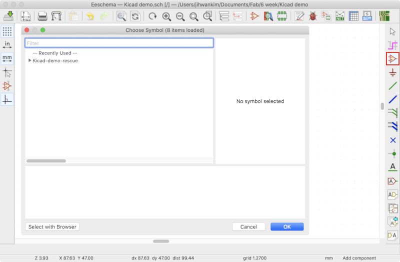
- Clicked 'Place symbol' butten located on right side of screen and clicked screen. But No symbol showed up in my mac. Only Mac users of our fablab students had the problem. Our library was empty.
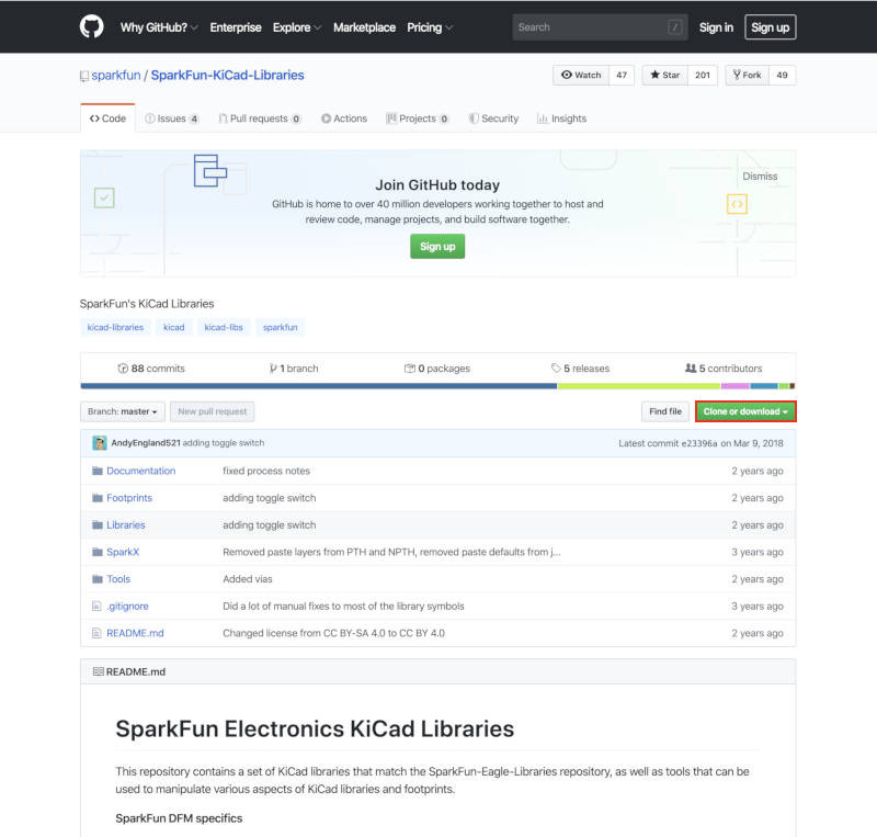
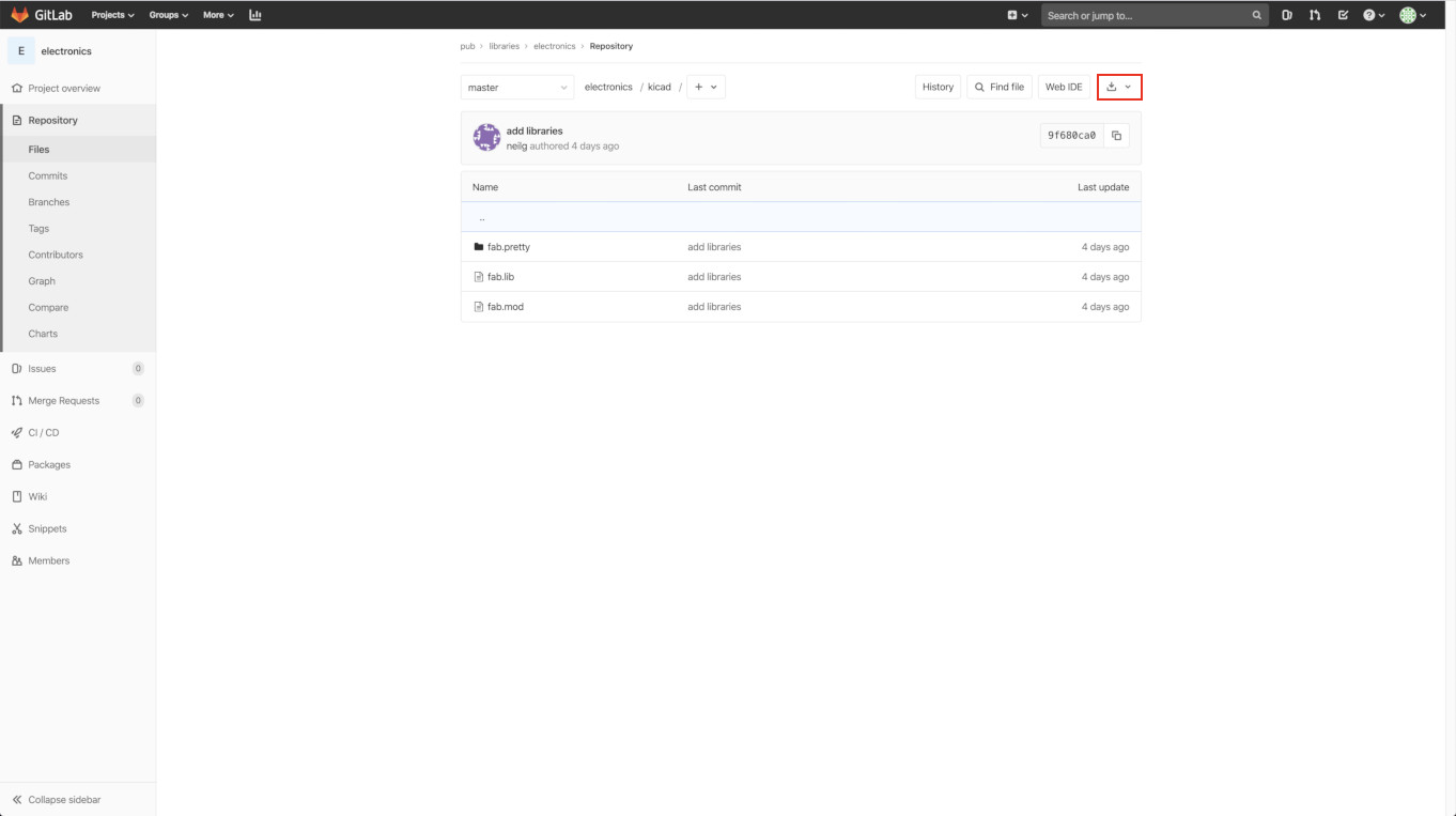
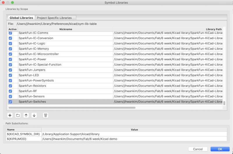
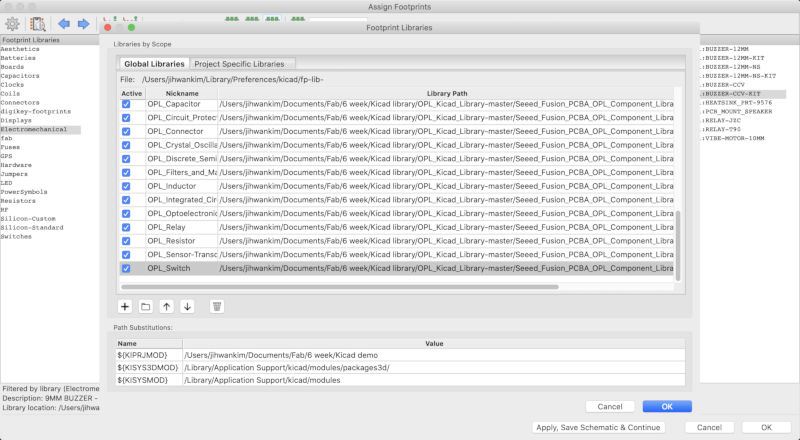
- So we searched 'mac kicad library' and downloaded Kicad library according to the library download page in Kicad site. And We downloaded sparkfun, fab(search 'pub' in Gitlab Site - click 'pub / libraries / electronics' - click 'kicad' - download), digikey, seeed libraries as well as kicad.


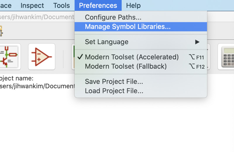
- Preferences - Manage Symbol Libraries - Add existing library to table - selected lid files in libraries downloaded
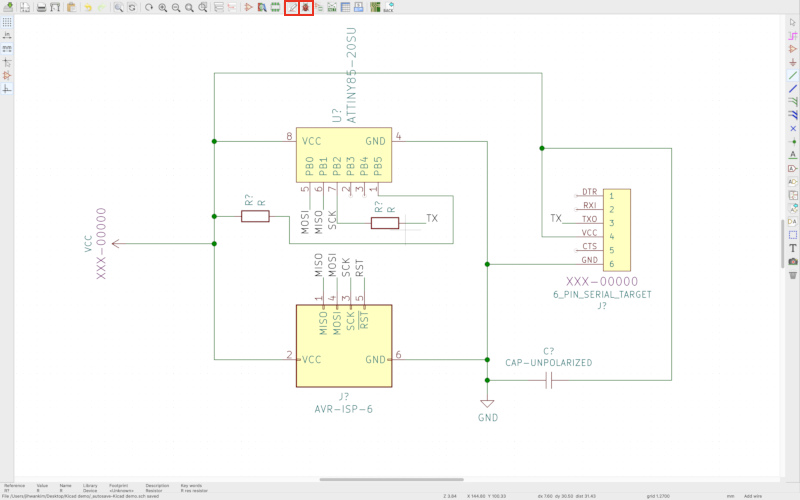
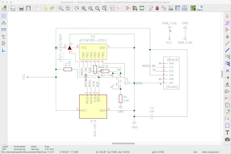
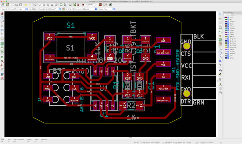
- We chose the ATTiny45 board as reference image to redraw. And then redrew ATTiny45 board in Kicad program according to Craig.(Ref. Used ATTiny85 instead of ATTiny45. The main difference between them is the amount of memory.)
- Used 'Select item', 'Place symbol', 'Place wire' and 'Place net label' button.

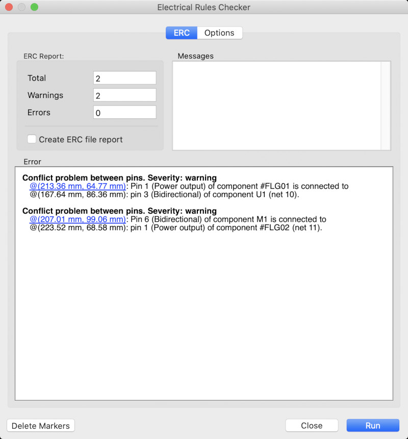
- Finished to redraw the board. Clicked 'Annotate schematic symbols' and 'Perform electrical rules check'.
- There were 8 errors
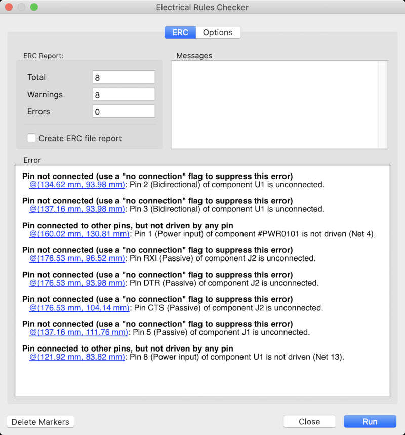
- 2 errors was that power didn't connected and 5 errors was that 'no connected' flag didn't set. finally, The last error was that one pin was not connected.
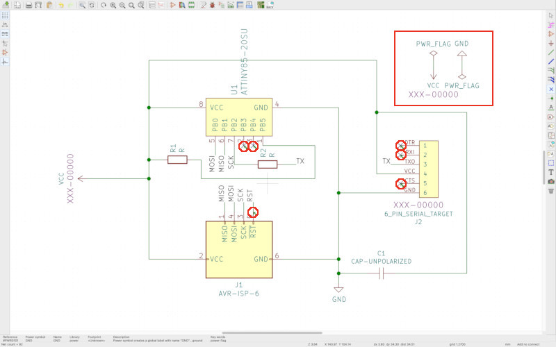
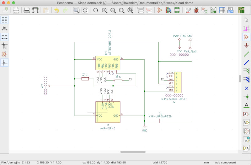
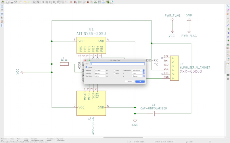
- And needed to set values of registers and capacity. then used 'v'key.
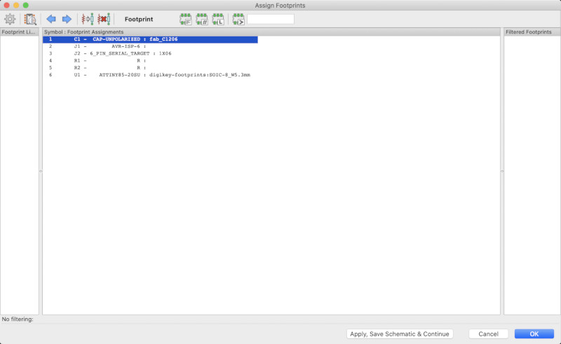
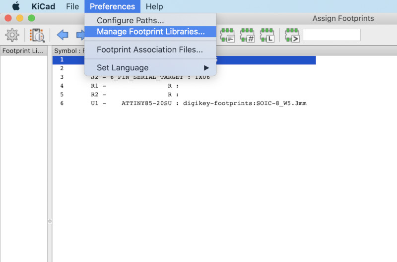
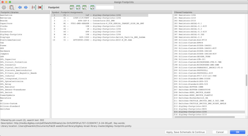
- Assigned PCB footprint to schematic symbol. Important to double click a choice and save schematic before closing the footprint screen.(Then mac users had problem again. We needed to add footprint libraries.)
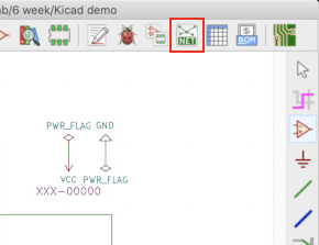
- Saved the net file after clicked 'Generate netlist'.
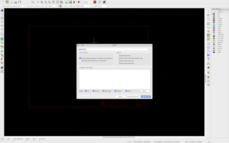
- Ran PCBnew.
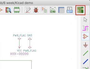
- Open netlist file in the PCBnew window. and joined these component by using 'Route tracks', 'Add graphic line'.
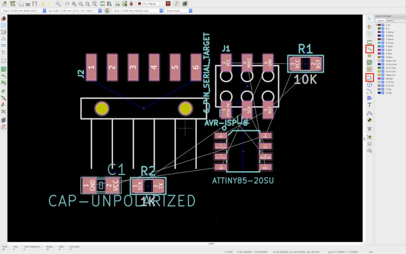
- But needed to add other component for assignment. Decided to add blue led and switch.
- Searched 'arduino [component name] sch' and find the most effective design to add component.
- Finished connecting component in PCBnew window. And then changed layer to 'Edge.Cut' and draw cut line.
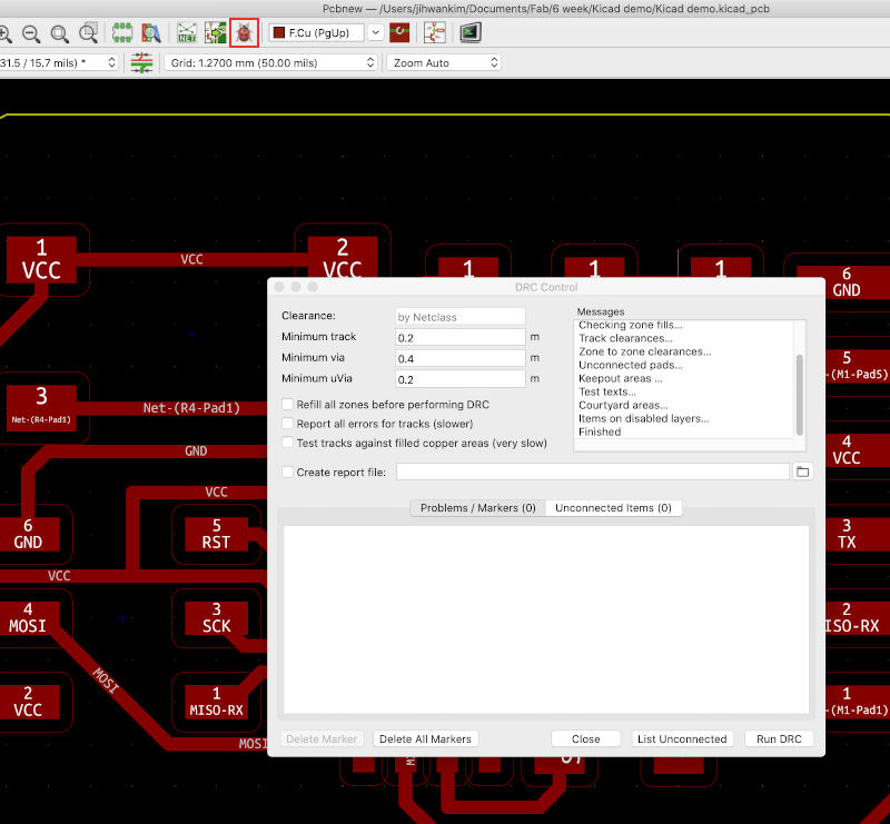
- Check error to perform 'Perform design rules check' To my surprise, No problem was found.
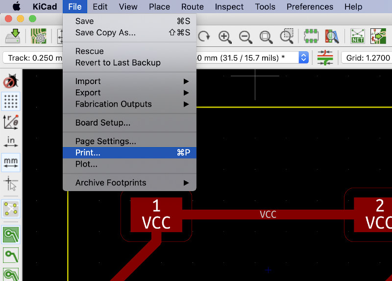
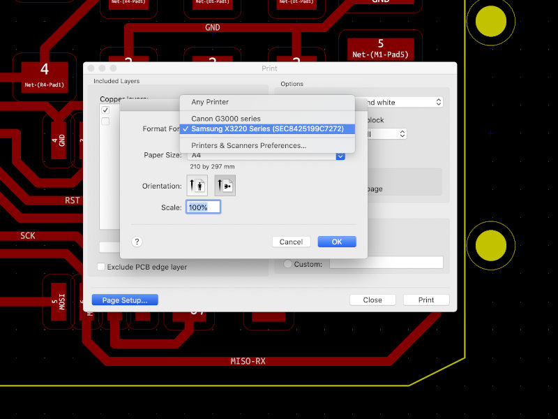
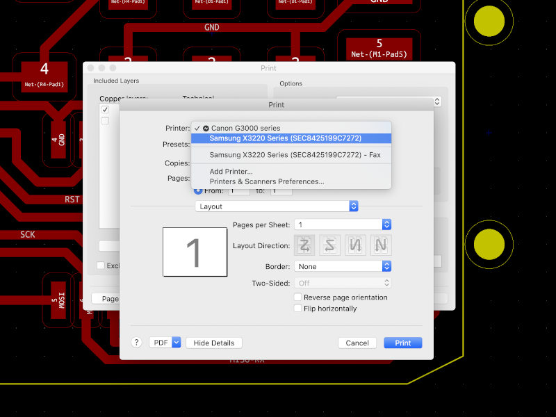
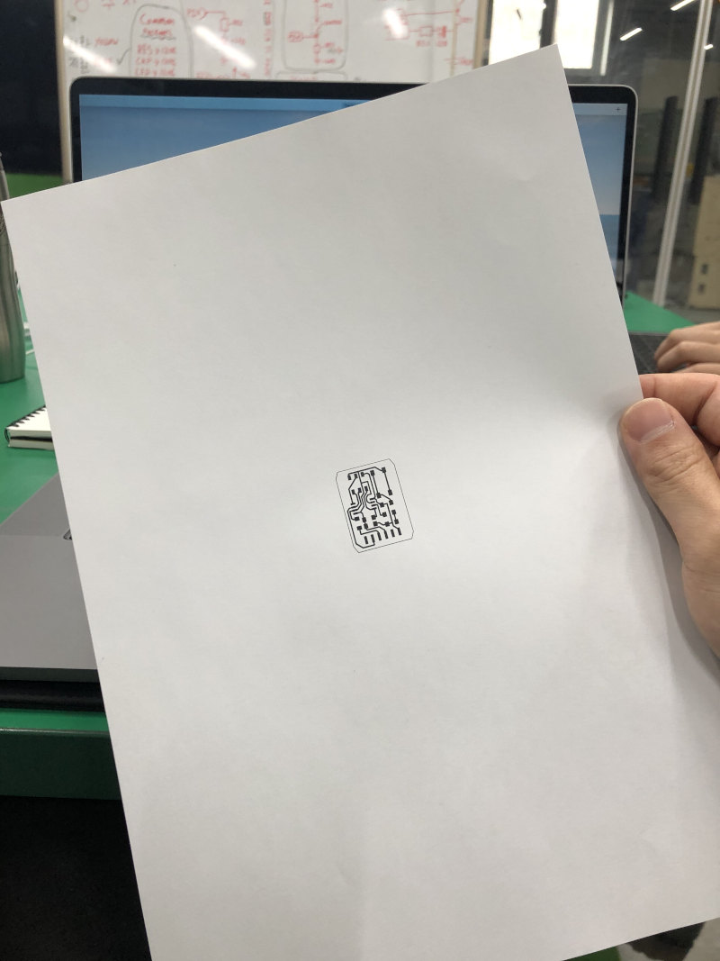
- So tried to print my design. but I failed because I saved file by using plot and put it in the USB and connected USB to the printer. The result was not good. (It wasn't until the next day that I knew. The way to print is using print button After set up the printer I want to use.)
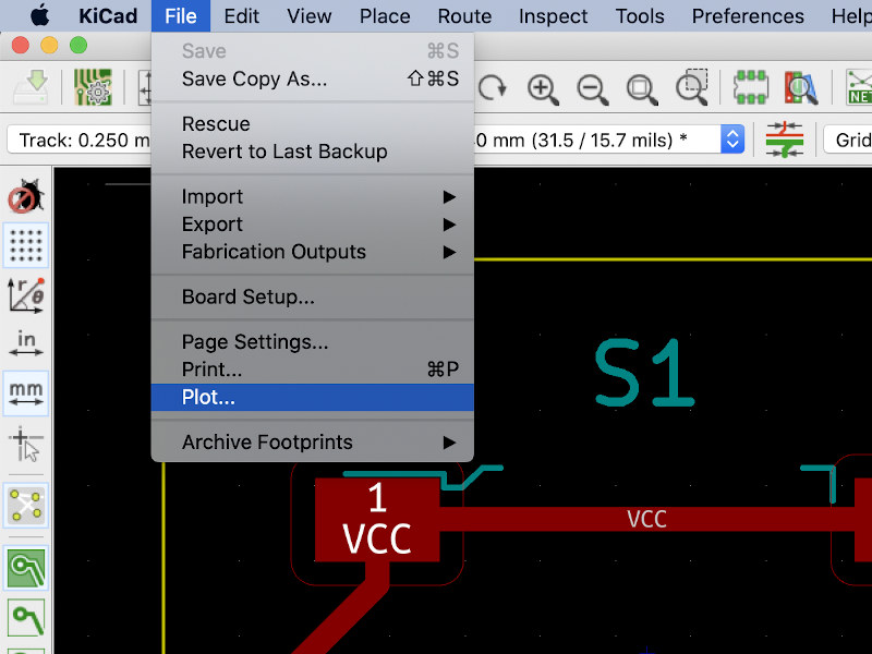
This process is very important. Because We can ensure that components and boards fit well and therefore we can prevent board waste.
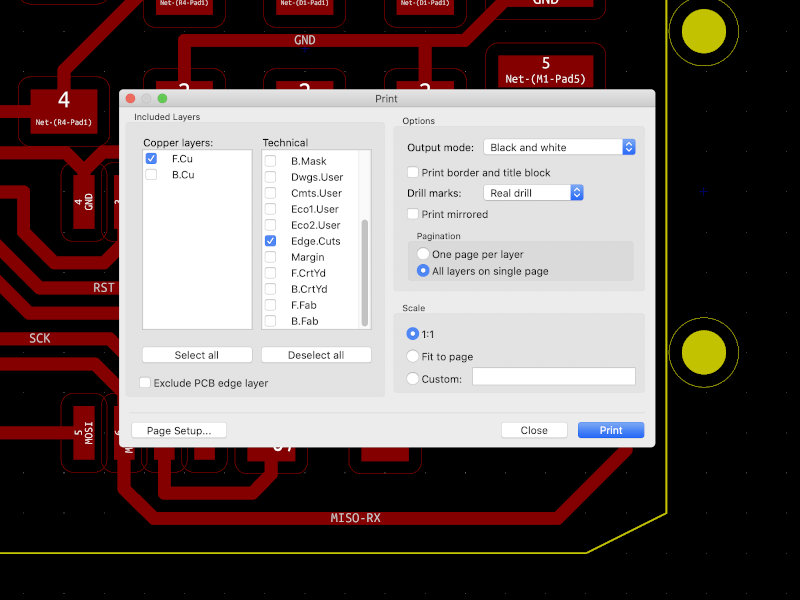
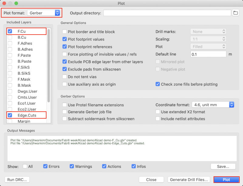
- Enter 'Plot' window - select layers (F.Cu, Edge.Cuts) - select format (gbr) - Click 'Plot'
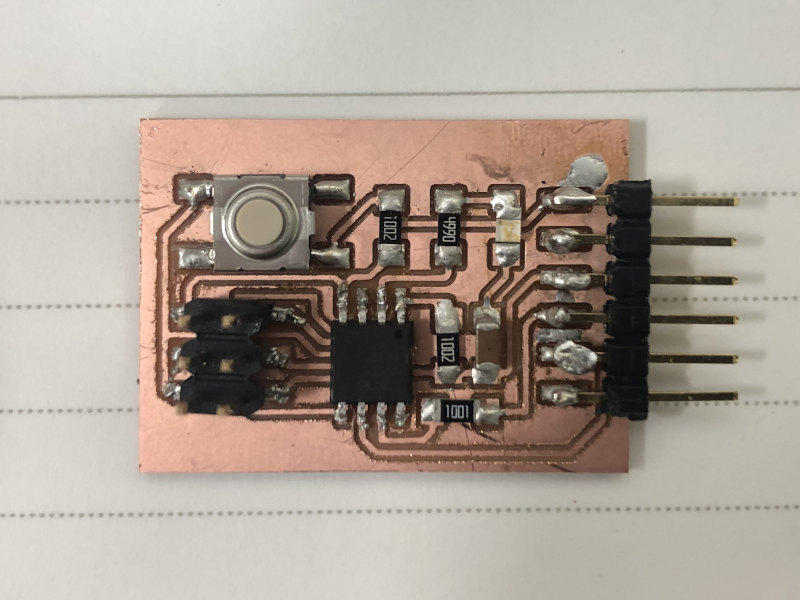
- Cut the circuit board using bantam tool. and soldering. (I followed the milling process of electronics production week.)
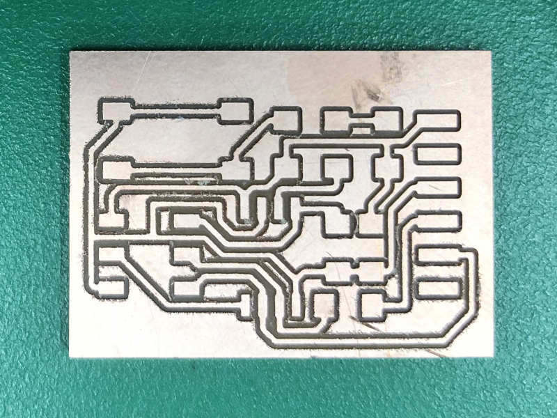
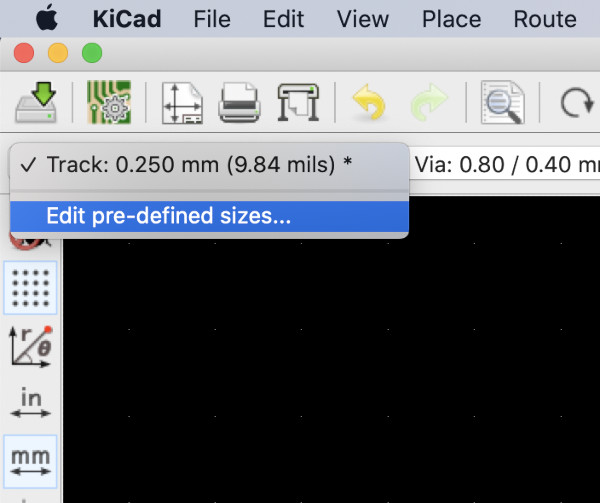
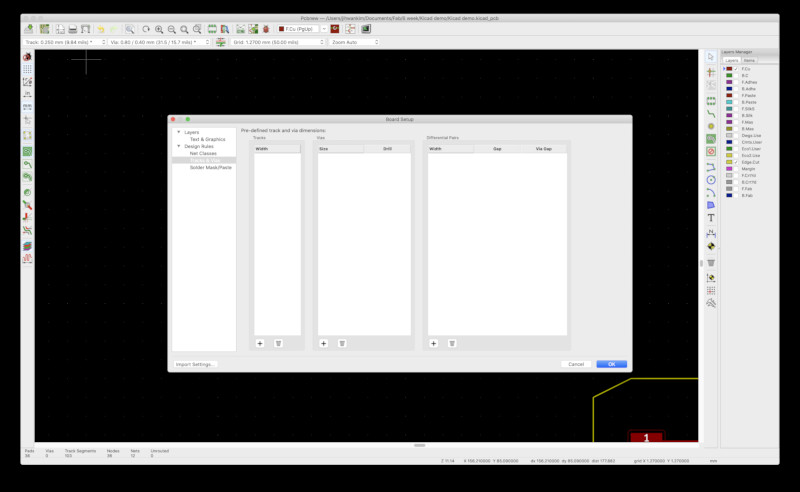
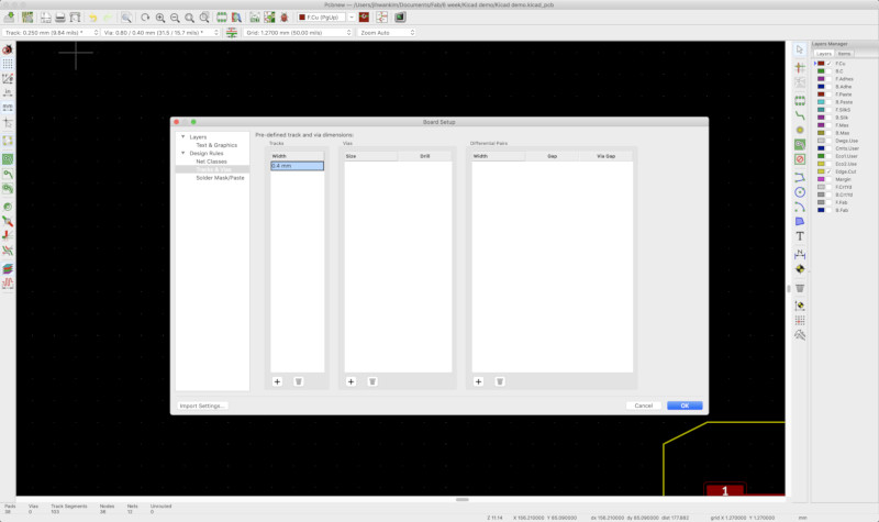
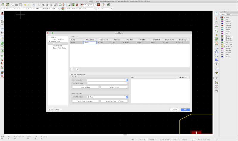
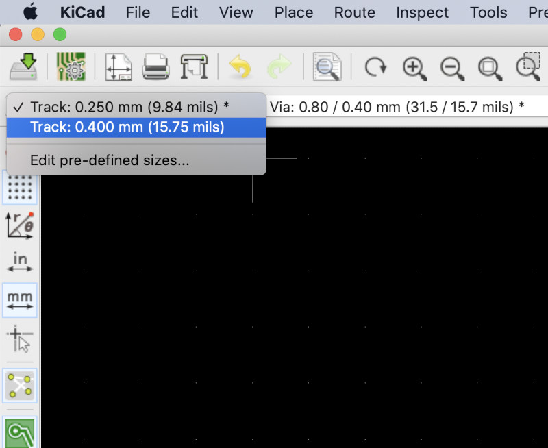
- In addition, I add a way to change the thickness of the line in PCBnew. The thickness is changed according to the endmill you have. I made an additional line of 0.4mm thickness and set the Clearance to 0.4mm in the default setting. This is because engraving endmill thickness is 0.4mm in our fablab.

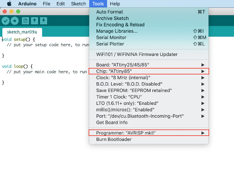
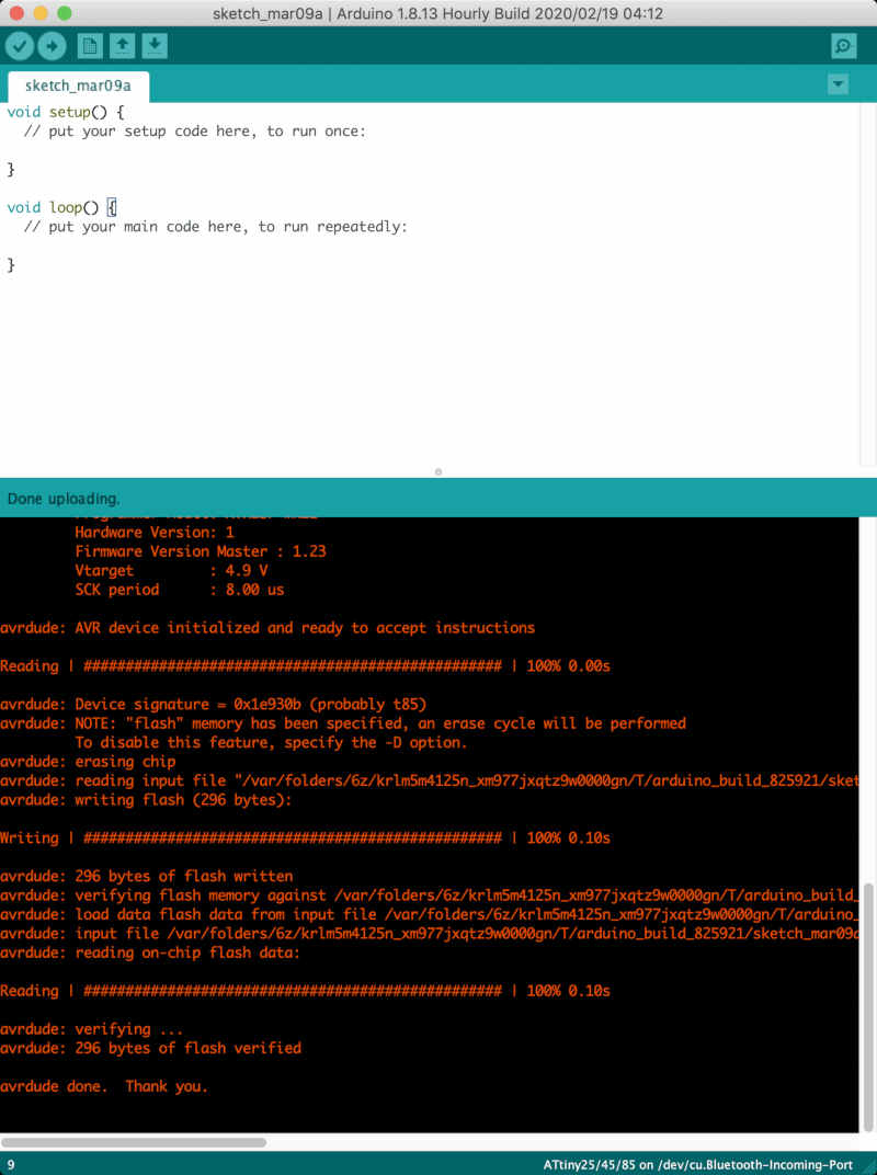
Programming
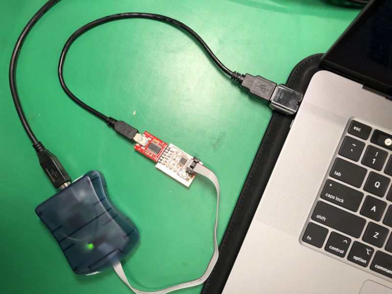
This problem later turned out to be a soldering problem. So I made sure to solder the ATtiny44 microcontroller part of my ISP board and the problem was solved.