Week 08 — Electronics Production
Group assignment
- Characterize the design rules for your in-house PCB production process: document the settings for your machine.
- Document the workflow for sending a PCB to a boardhouse.
- Document your work to the group work page and reflect on your individual page what you learned.
Individual assignment
- Make and test a microcontroller development board that you designed.
Learning outcomes
- Describe the process of tool-path generation, milling/laser engraving, stuffing, de-bugging and programming.
- Demonstrate correct workflows and identify areas for improvement if required.
Checklist
- Linked to the group assignment page
- Documented how you made the toolpath
- Documented how you made (milled, stuffed, soldered) the board
- Documented that your board is functional
- Explained any problems and how you fixed them
- Uploaded your source code
- Included a hero shot of your board
Documentation
Introduction
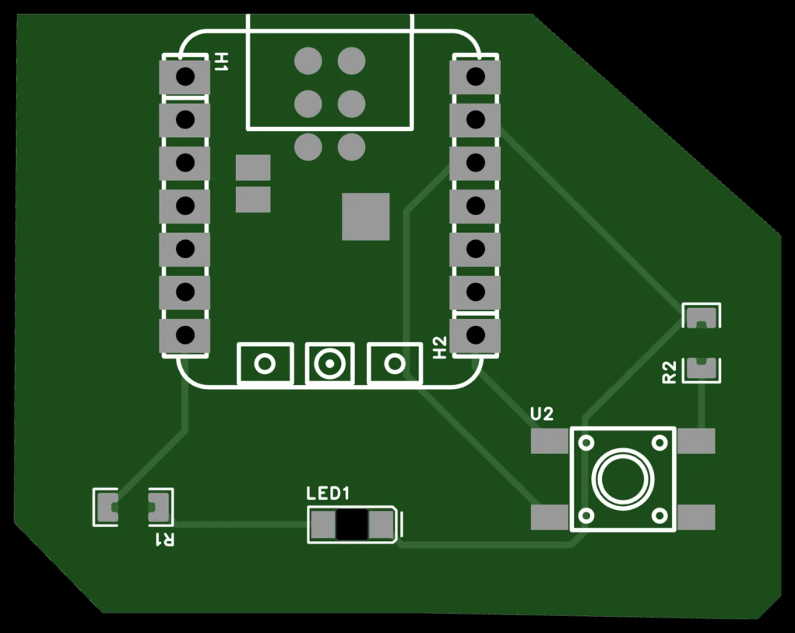
Electronics production week focused on making custom printed circuit boards (PCBs) using CNC milling – a process called PCB isolation routing. Instead of chemical etching, a precision CNC machine physically mills away thin channels of copper from a copper-clad board, leaving behind the circuit traces.
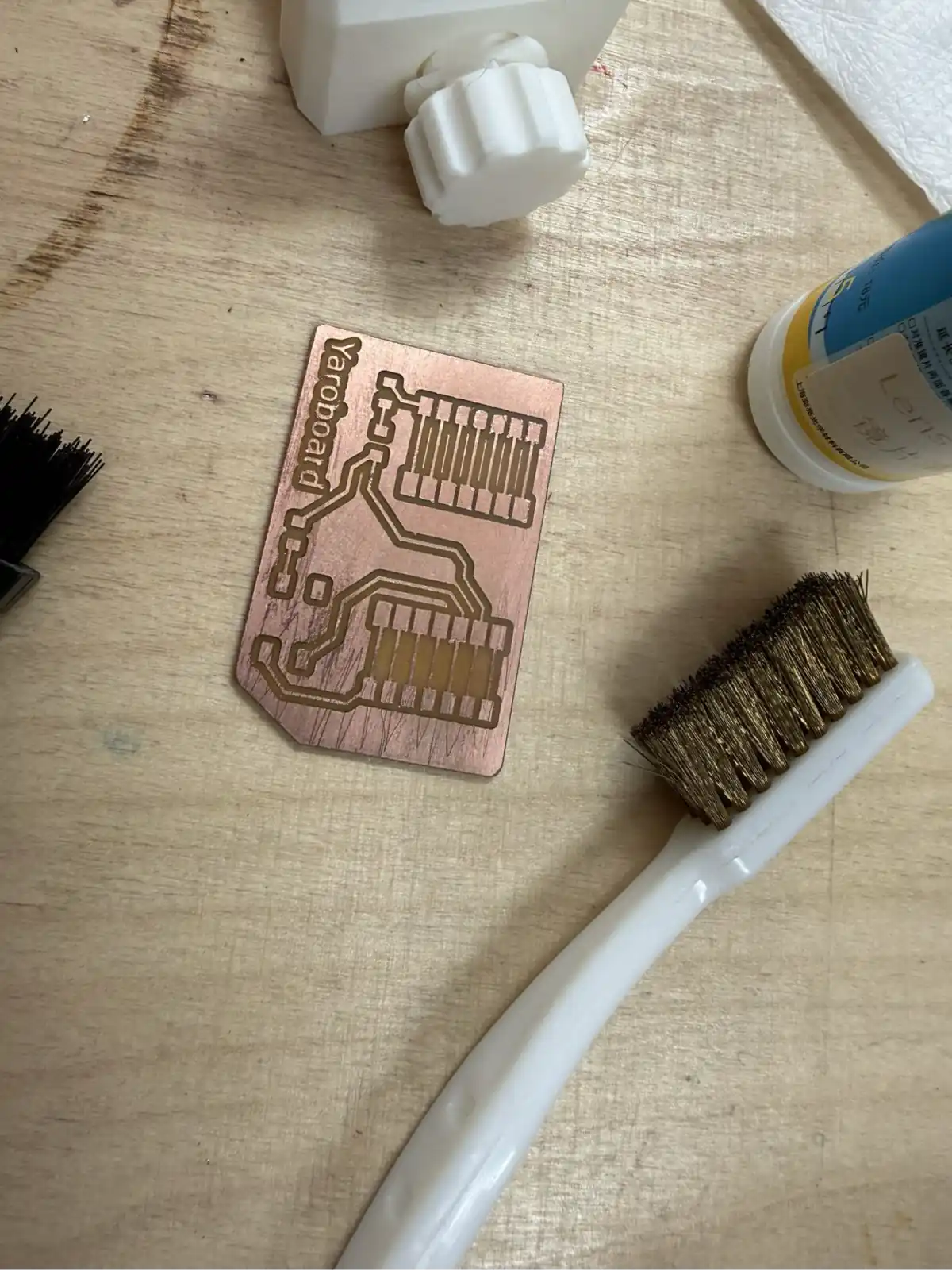
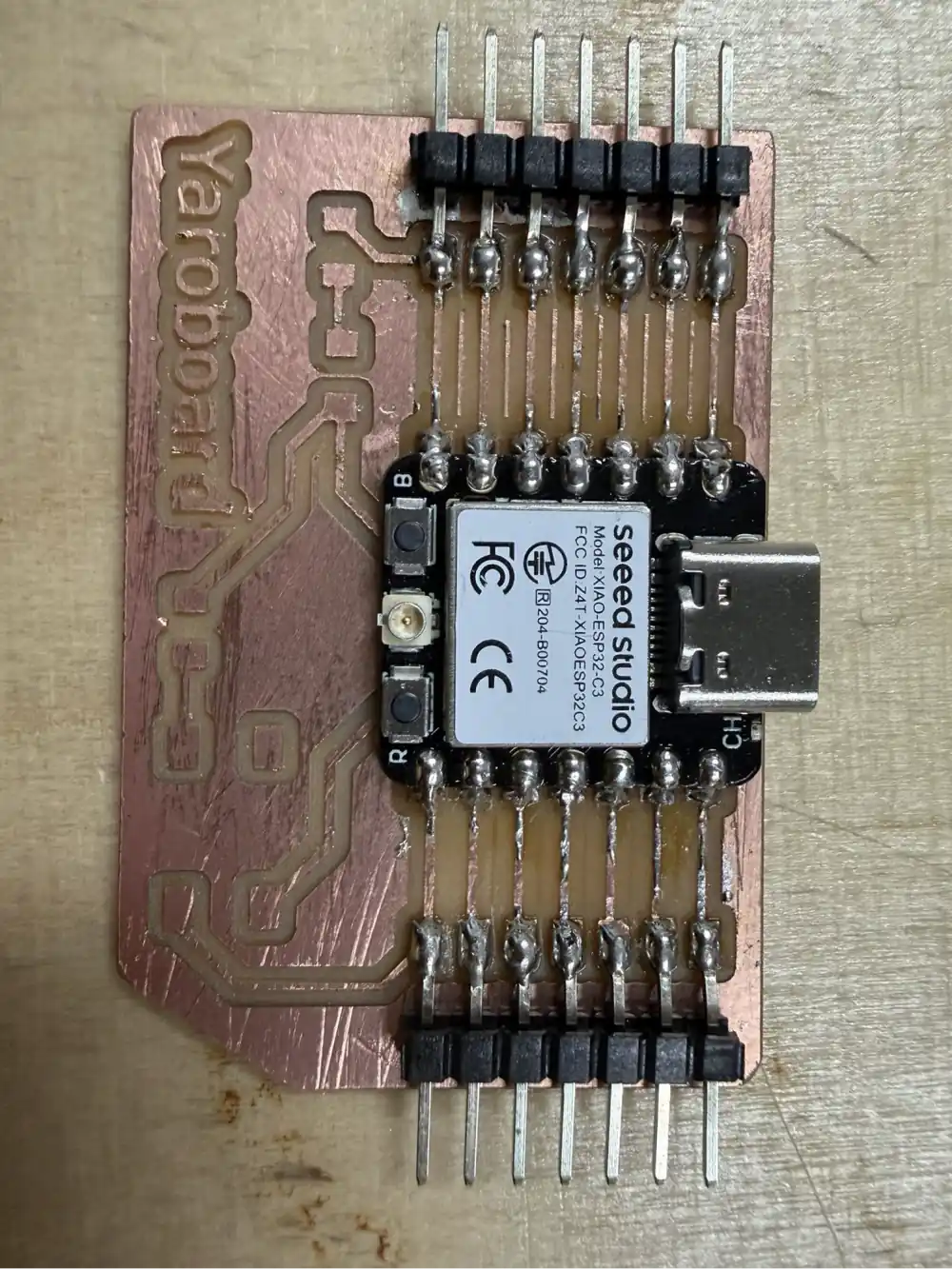
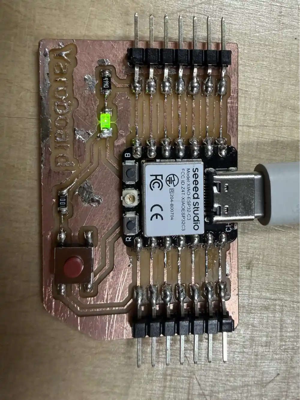
By the end of the week the goal was to have a fully milled, populated, and working PCB – the "Yaroboard" – a custom breakout board for the Seeed Studio XIAO ESP32 C3 microcontroller.
From Week 6 design to Week 8 production
In Week 6 Electronics Design, I designed a simple PCB with a button and an LED for the Xiao microcontroller. For Week 8, I prepared the manufacturing files and reviewed the full PCB production workflow.
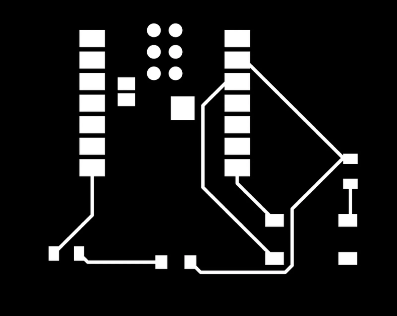
The main production file for this board is available here: ProPrj_W8 Elec Production_2026-06-01.epro. This EasyEDA project file contains the board design I used to prepare the production outputs for milling and fabrication.
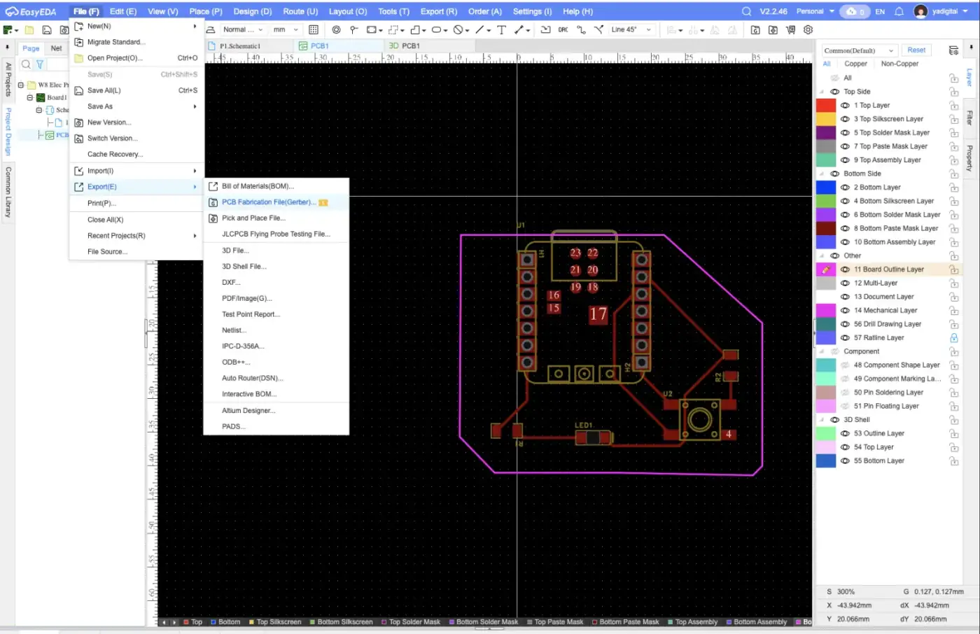
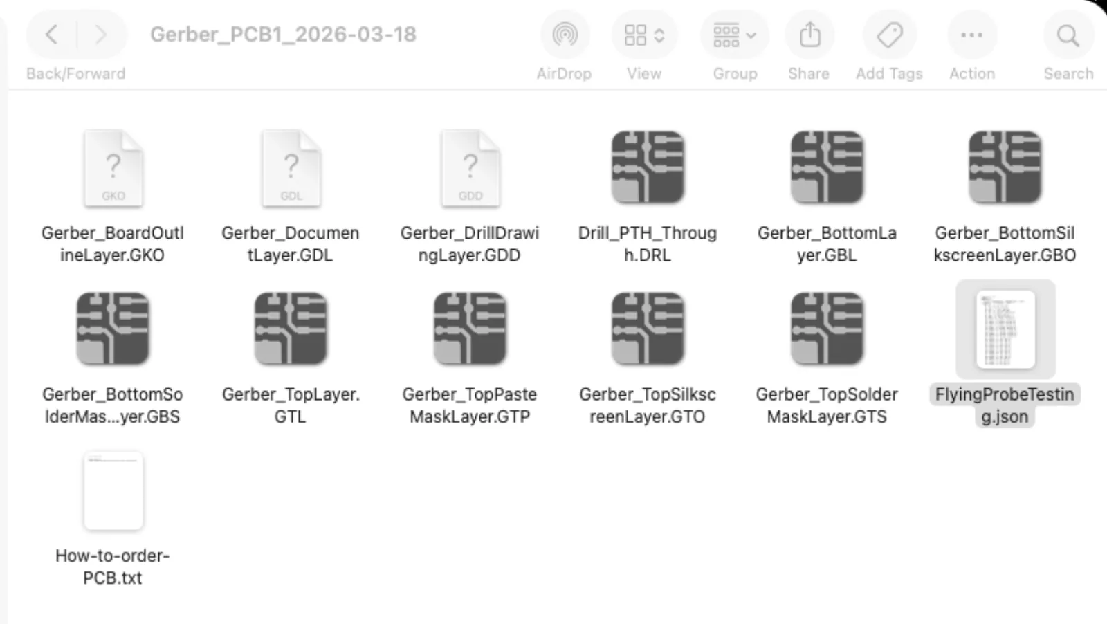
Here's a quick rundown of each file in the Gerber export:
Board definition
- GKO (BoardOutlineLayer) — defines the physical edge/shape of the PCB
- GDL (DocumentLayer) — notes, dimensions, or annotations not related to manufacturing
Copper layers
- GTL (TopLayer) — copper traces on the top of the board
- GBL (BottomLayer) — copper traces on the bottom of the board
Solder mask (the colored coating with openings for pads)
- GTS (TopSolderMaskLayer) — openings in the top solder mask
- GBS (BottomSolderMaskLayer) — openings in the bottom solder mask
Silkscreen (the printed labels/outlines you see on the board)
- GTO (TopSilkscreenLayer) — component labels and markings on top
- GBO (BottomSilkscreenLayer) — component labels and markings on bottom
Paste mask (used for stencil-based SMD soldering)
- GTP (TopPasteMaskLayer) — where solder paste gets applied on top pads
Drill files
- DRL (Drill_PTH_Through) — locations and sizes of all plated through-holes (PTH) — vias and component holes
- GDD (DrillDrawingLayer) — visual drawing of drill holes for reference
Extras
- FlyingProbeTesting.json — test point data used by flying probe testers to verify electrical connections after manufacturing
- How-to-order-PCB.txt — EasyEDA's instructions for submitting this package to a fab house (like JLCPCB)
I found the resource on how to convert the Gerber site into PNG from FabLab Kerala.
https://gerber2png.fablabkerala.in/
After study documentation from Namita
https://fabacademy.org/2025/labs/kochi/students/namita-aravind/assignments/week08.html
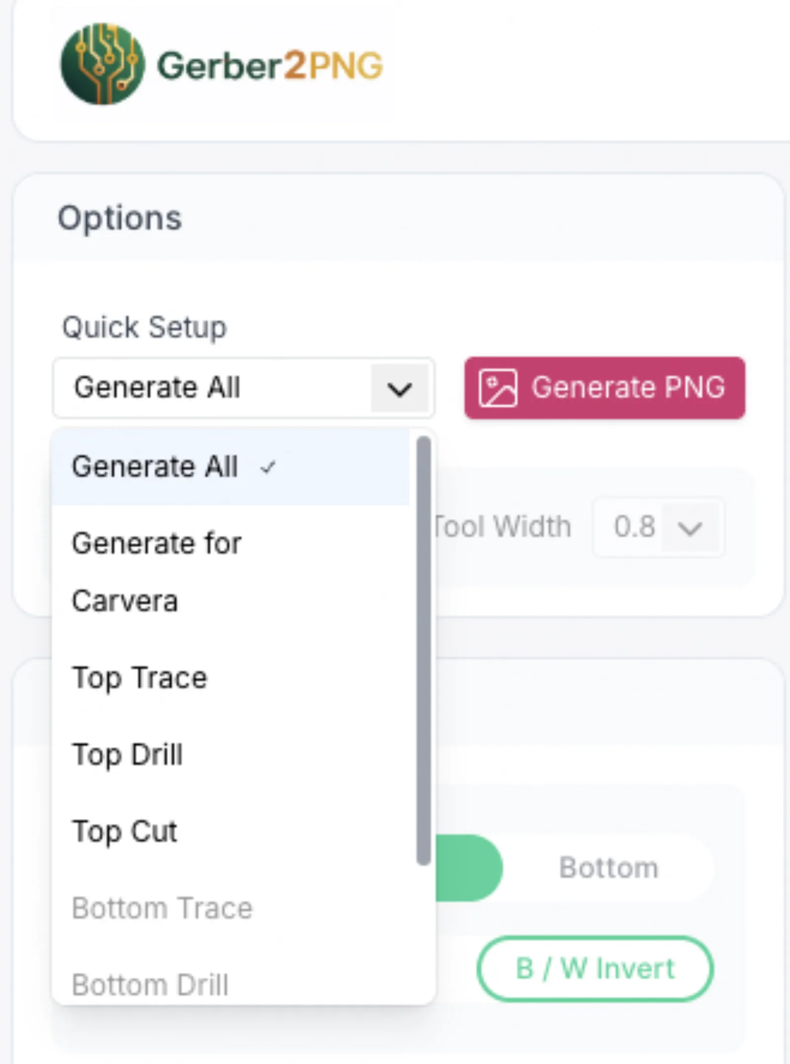
I uploaded all files and selected option “Generate All” then “Generate PNG”.
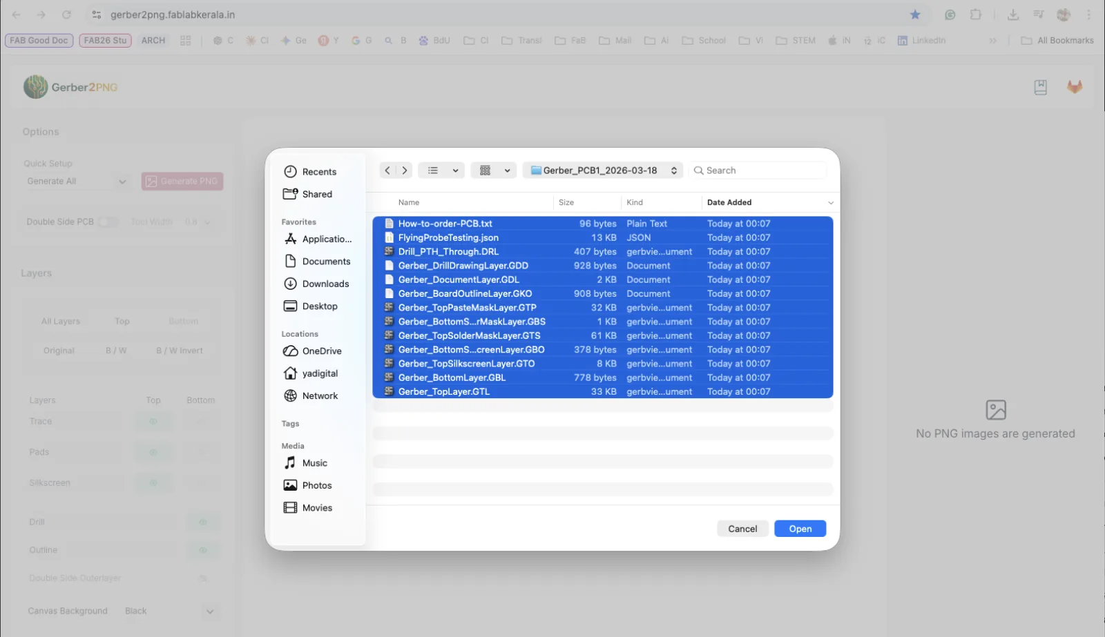
Website generated four files:
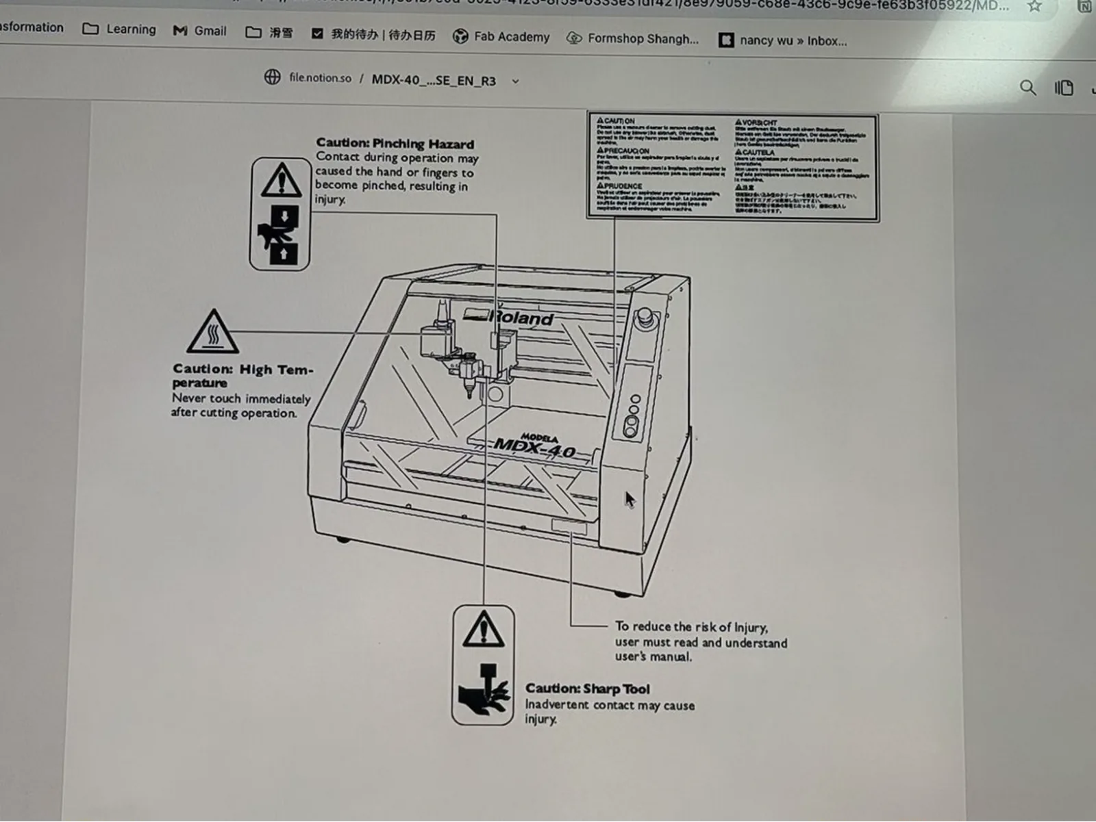
Equipment Overview
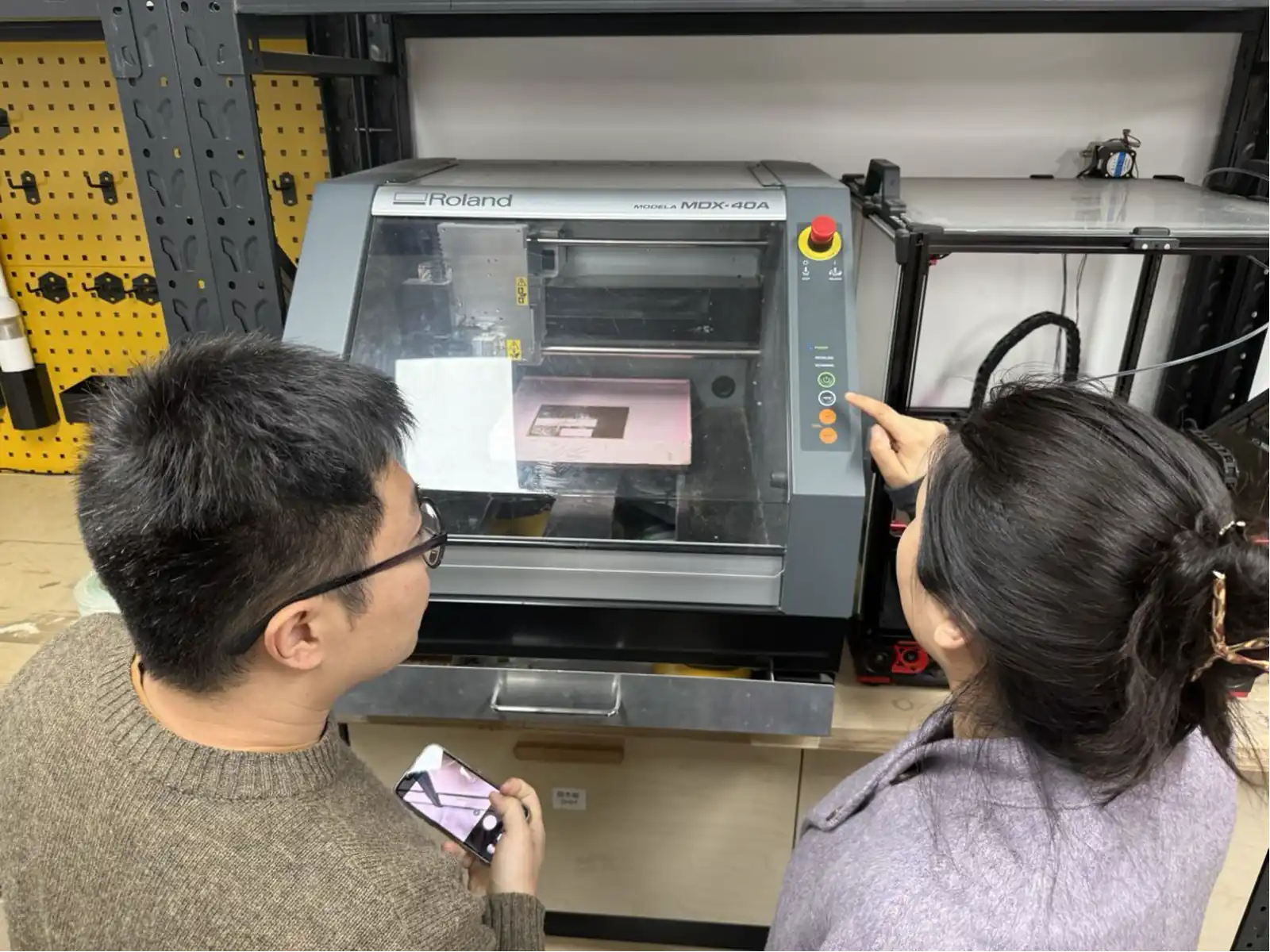
Roland MDX-40A – Professional PCB Mill
The main machine used for PCB milling at the FormShop Fab Lab is the Roland MDX-40A – a compact, high-precision desktop CNC milling machine. It is operated through Roland's VPanel software using the RML-1 control language. The machine is capable of milling traces and gaps as narrow as 0.1 mm, making it ideal for fine-pitch PCB work.
Researching CNC Milling Options
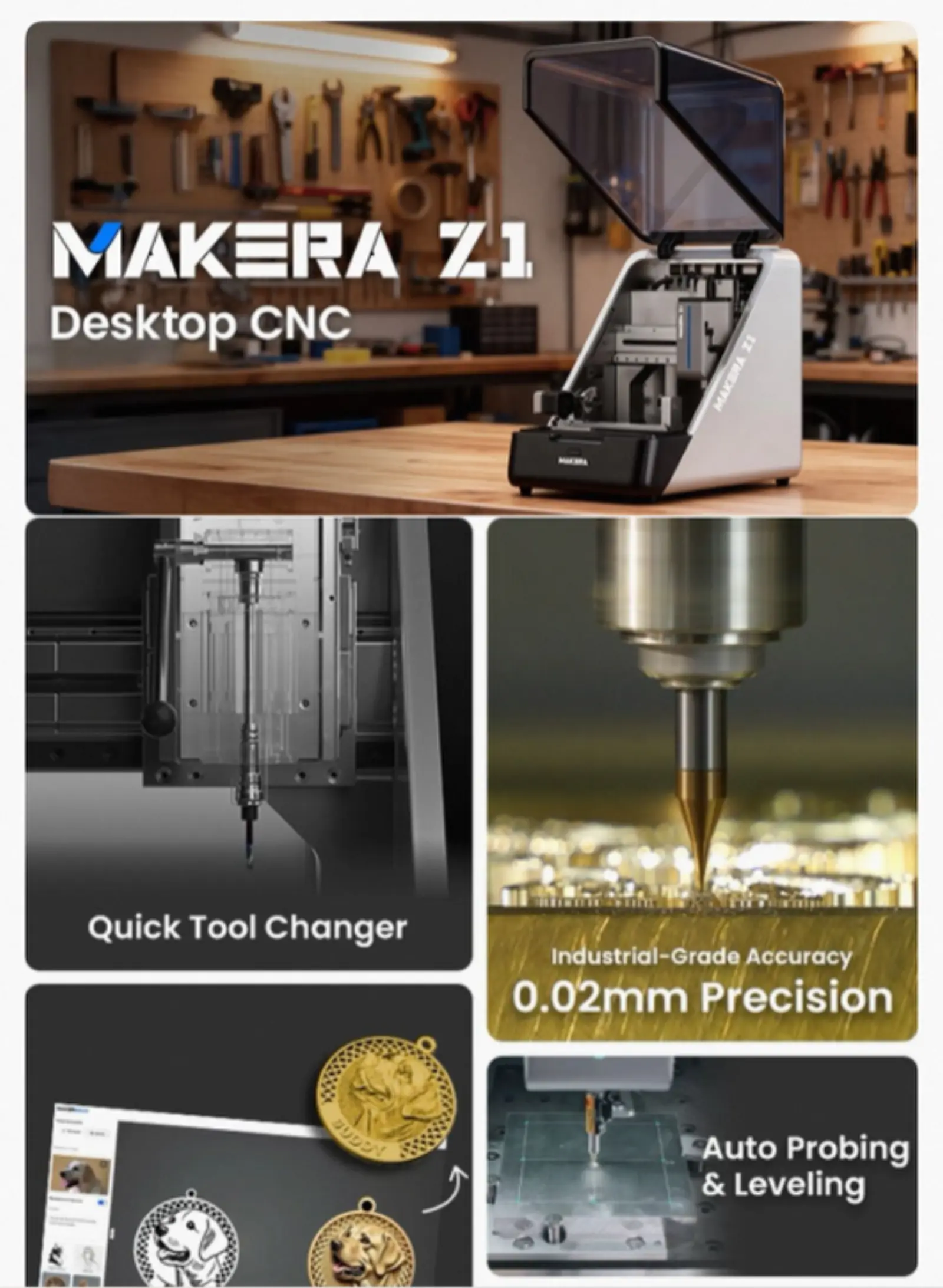
As part of the research phase, other PCB milling machines on the market were explored. The Roland MDX-40 (the older 4-axis variant) is available second-hand at significantly lower cost. The Makera Z1 Desktop CNC is a newer option with an automatic tool changer and 0.02 mm industrial precision.
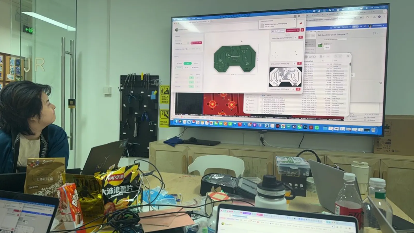
Class Design Review Session
A group review session was held with all students' PCB designs projected on a large screen using EasyEDA. The session covered DRC (Design Rule Checks), trace width and clearance settings, and the correct export process for sending files to the mill.
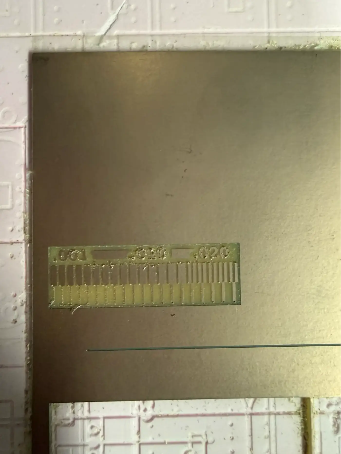
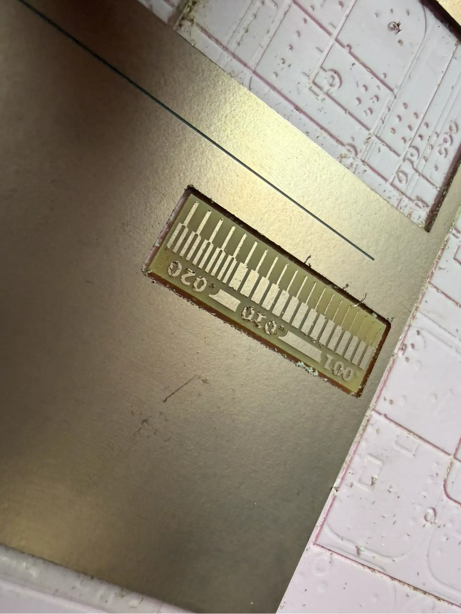
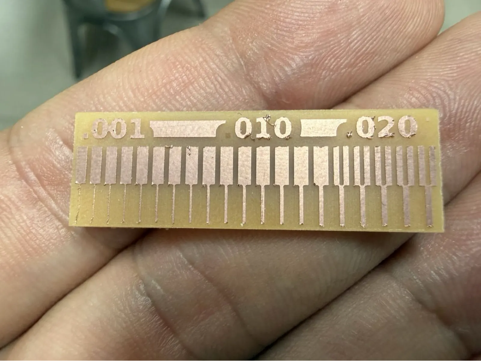
Trace Width Test
Before milling the actual board, a trace width test is mandatory. This test mills a small comb pattern with three different trace pitches to find the finest reliable trace width achievable with the current bit and machine settings.
The test piece shows three zones: 0.001", 0.010", and 0.020" trace-to-trace spacing. After milling, the test is inspected under magnification. The finest zone that shows complete, clean isolation (no copper bridges) determines the minimum design rule for this machine/bit combination.
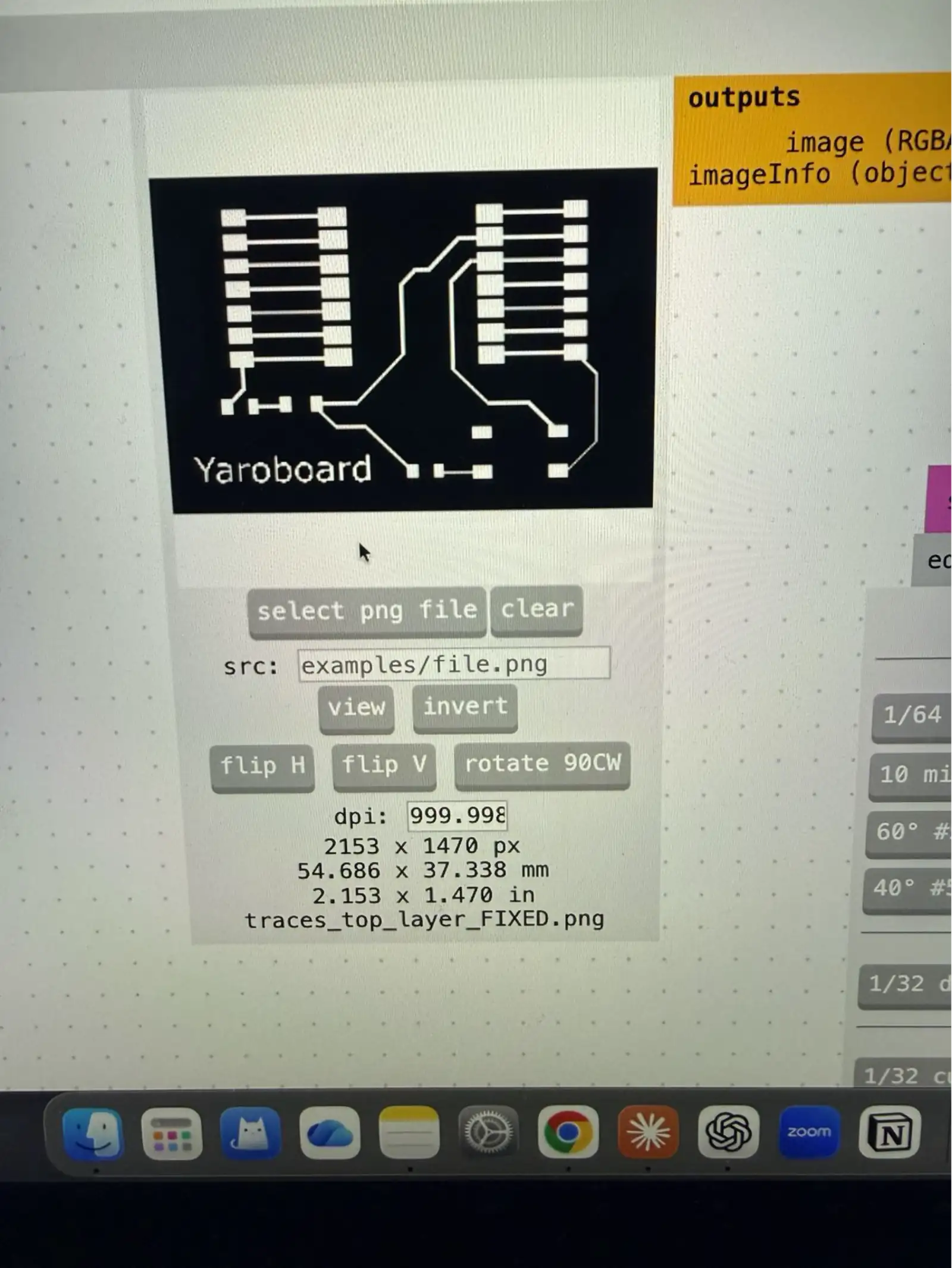
Design Preparation – Mods Software
The PCB design was created in EasyEDA and exported as a high-resolution PNG image of the copper trace layer. This image is then processed using Mods – a browser-based modular workflow tool used universally across Fab Labs. Mods converts the PNG bitmap into an RML (Roland Machine Language) or G-code file that the mill can execute.
Key export settings in Mods:
- DPI: 999 (high resolution for fine trace accuracy)
- Board size: 54.686 × 37.338 mm (Yaroboard dimensions)
- File: traces_top_layer_FIXED.png (pre-processed in image editor to fix any pixel artefacts)
- Cut depth: 0.1 mm for traces; 1.8 mm for profile cut
Machine Setup
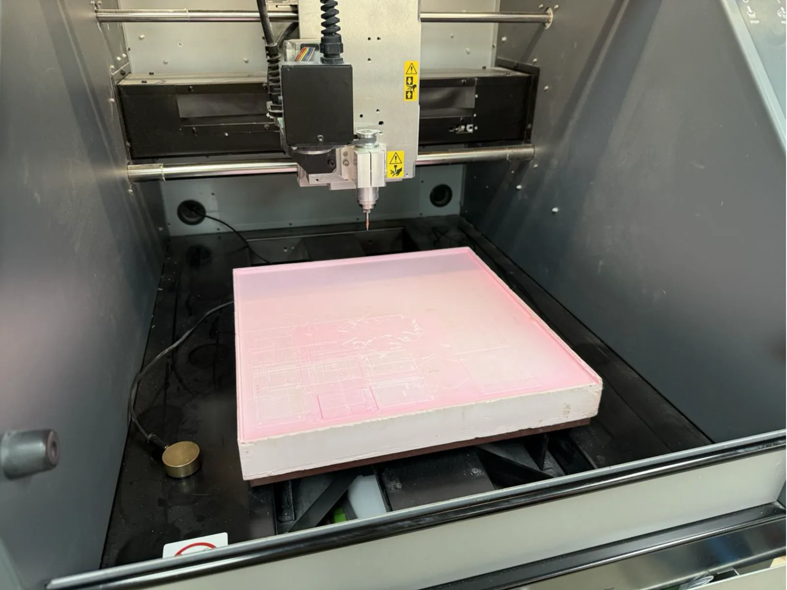
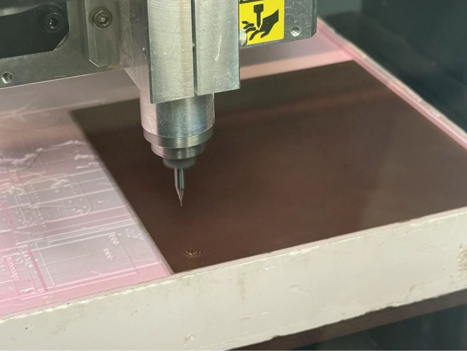
Loading the Copper Board
The cut copper-clad board is placed inside the Roland MDX-40A on top of a pink sacrificial foam layer. The foam protects the machine bed from the cutting bit when it passes through the full board thickness. The board is secured with double-sided tape on all four corners to prevent any movement during milling – even 0.1 mm of shift will cause misaligned traces.
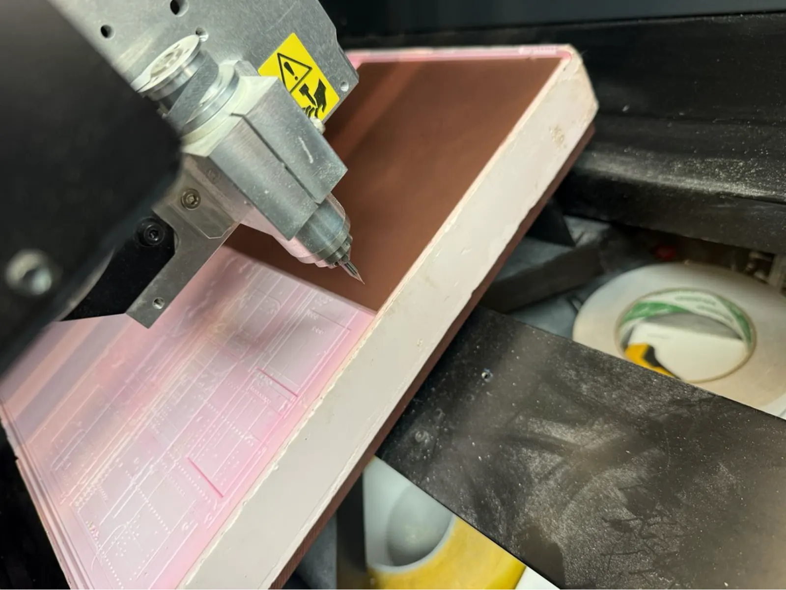
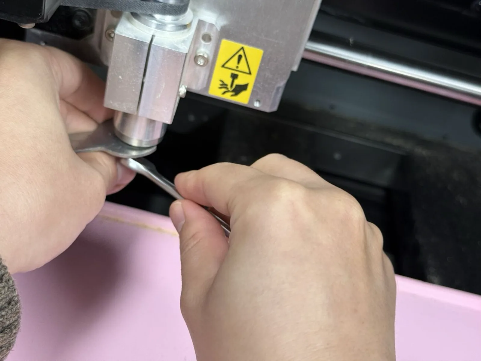
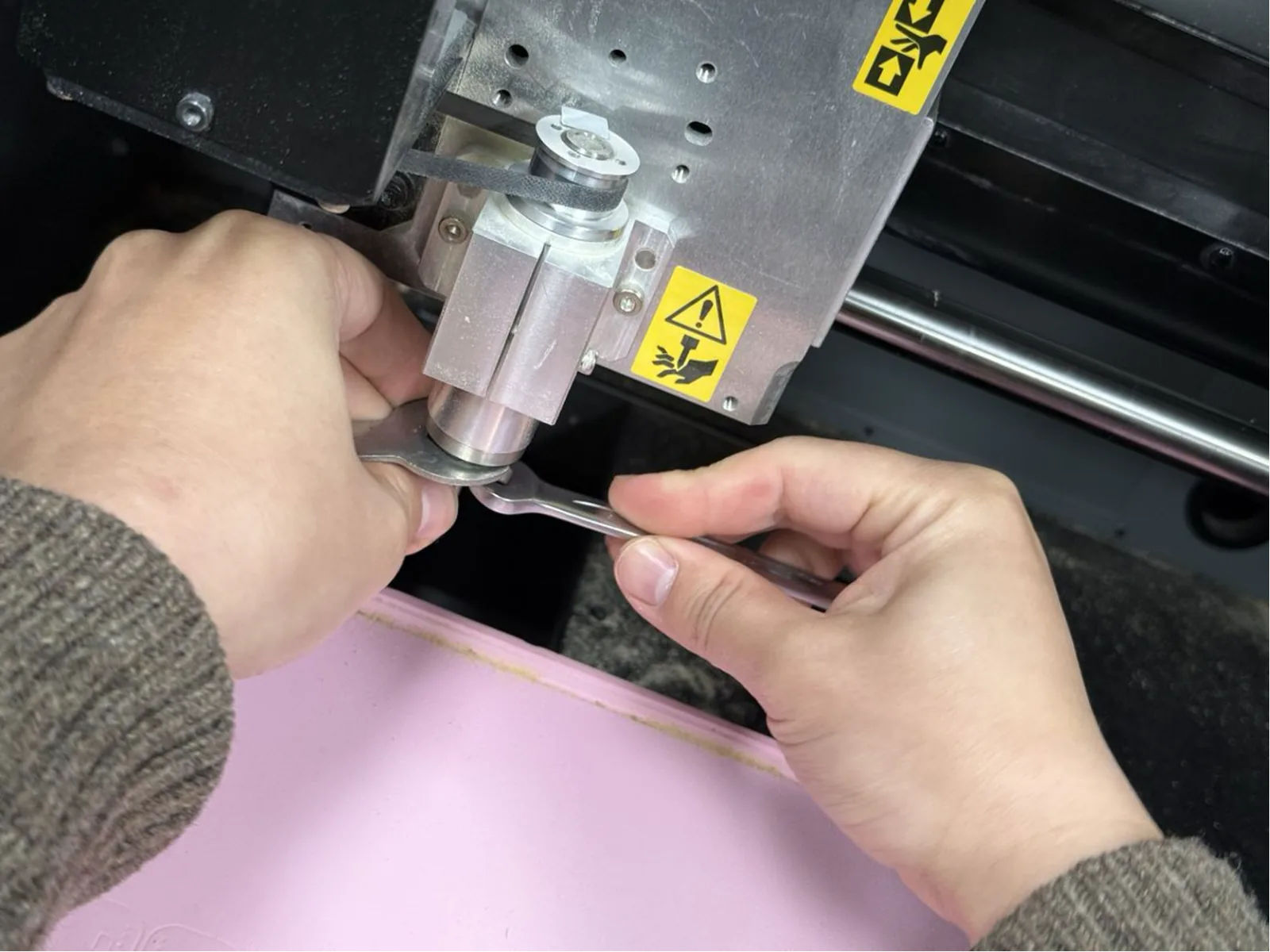
Installing the Engraving Bit
The V-bit engraving tool is installed into the Roland's precision collet using the included open-ended wrenches. The bit must be fully seated – the cutting tip should protrude by the minimum amount needed for the job. Any runout (wobble) in the bit will cause variable trace widths and potentially break the fragile bit tip.
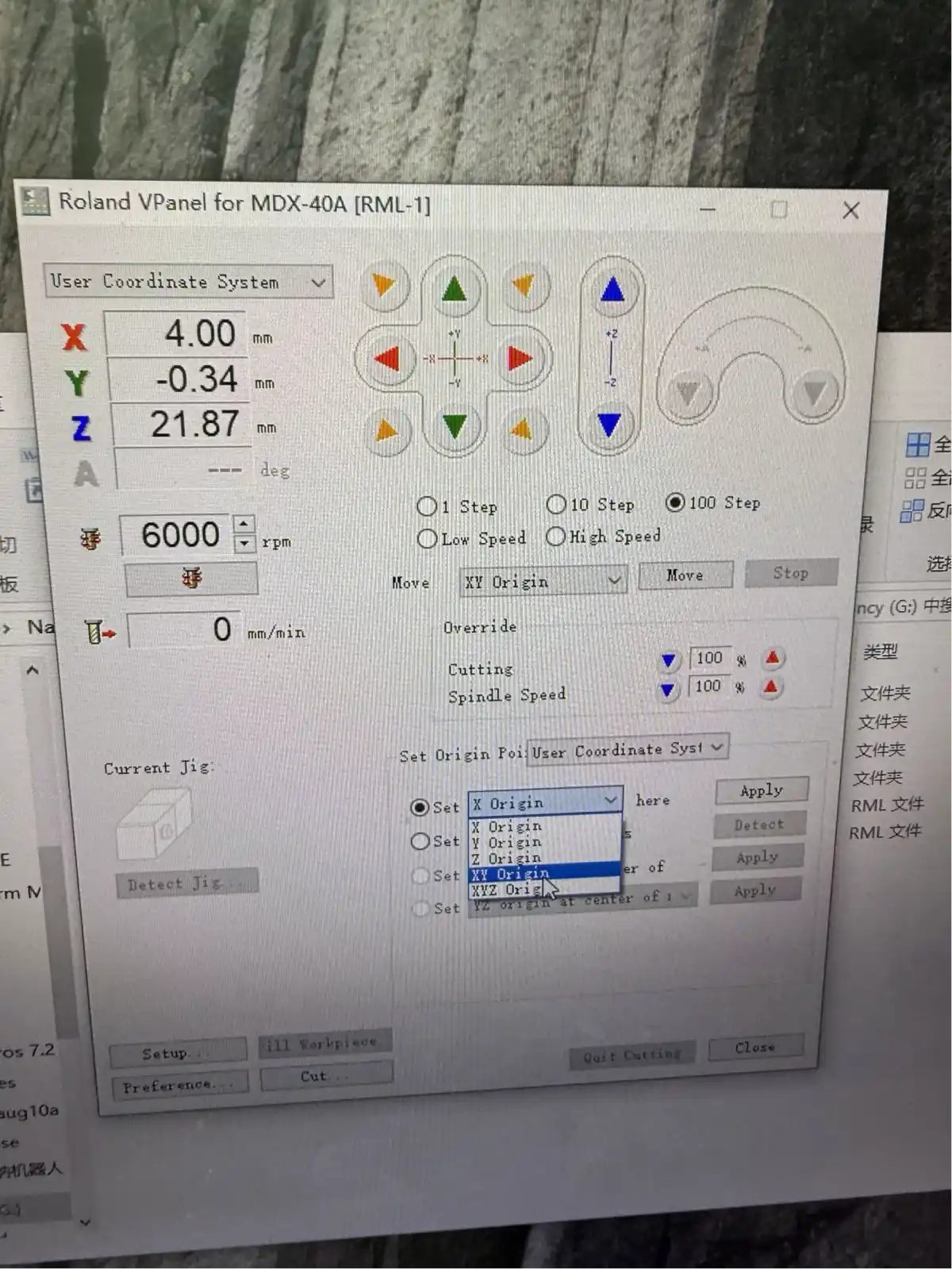
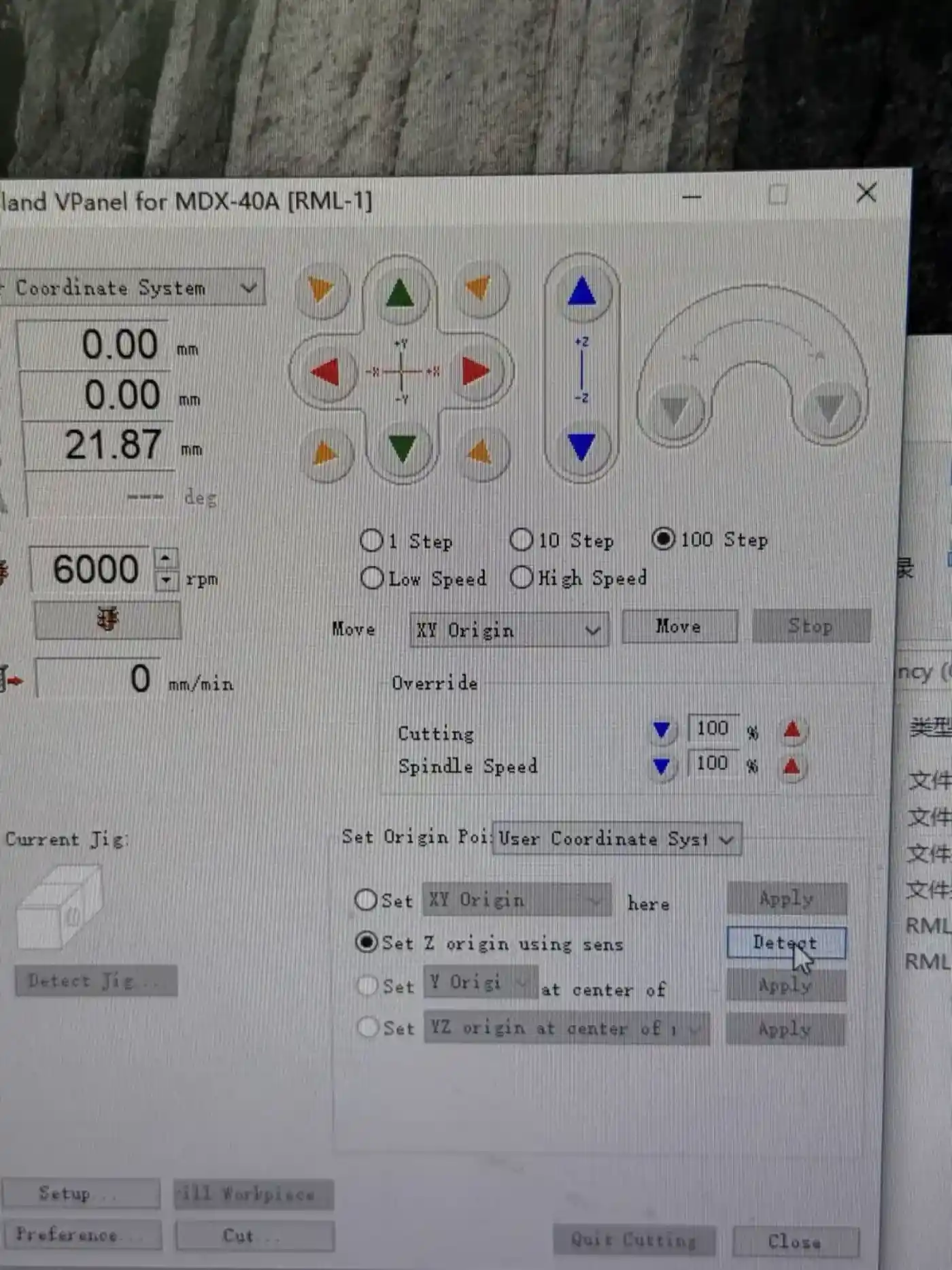
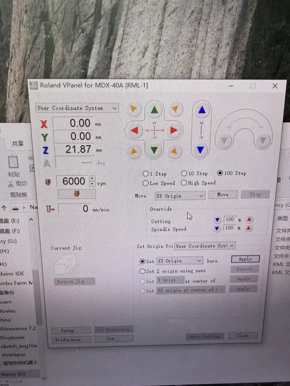
Setting Origins with Roland VPanel
The Roland VPanel (RML-1 interface) is the software used to manually jog the machine and set the work origins. The process is:
- Step 1: Jog the machine to the front-left corner of the copper board using the directional arrows in VPanel.
- Step 2: Press "Set XY Origin here" to register X=0, Y=0 at the board corner.
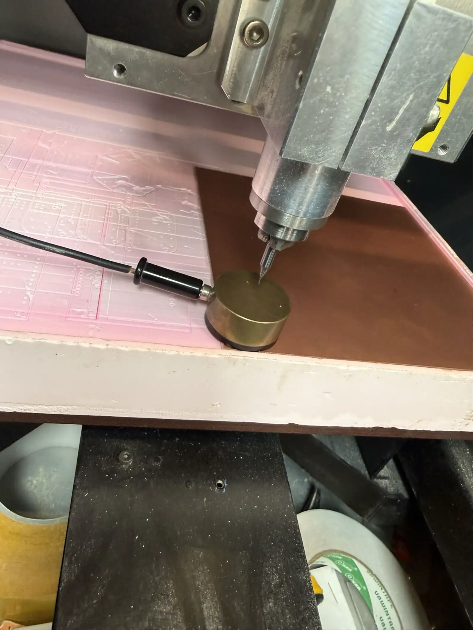
- Step 3: Place the Z-probe brass disc on the copper surface directly below the bit.
- Step 4: Select "Set Z origin using sensor" in VPanel. The machine lowers the bit slowly until it touches the brass disc, then records the exact Z height automatically.
- Step 5: Confirm all three axes read 0.00 mm before sending the job.
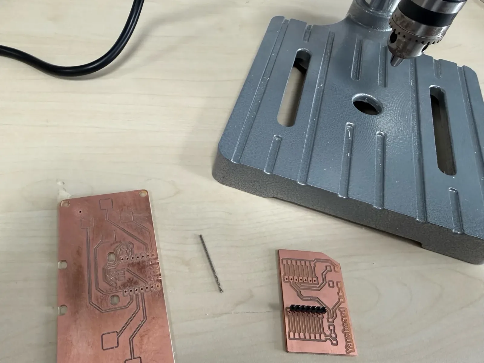
Milling the PCB
Running the Trace Milling Job
The trace milling job is sent from Mods (or Candle for G-code machines) to the Roland. The spindle spins at 6,000–10,000 RPM and the V-bit moves across the board, carving isolation channels through the copper layer. Fine copper-coloured dust accumulates on the board surface during the process.
It is important not to open the machine lid or touch the board during the job. Any vibration can cause the bit to skip, producing an open-circuit trace or a broken bit.
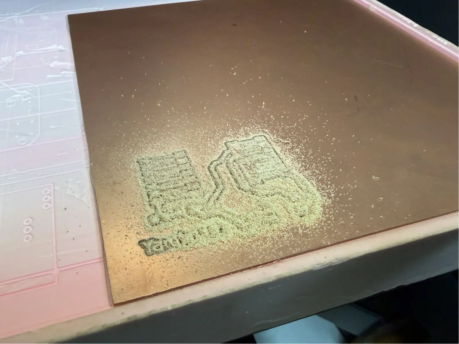
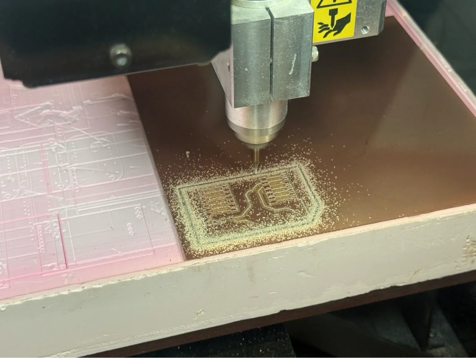
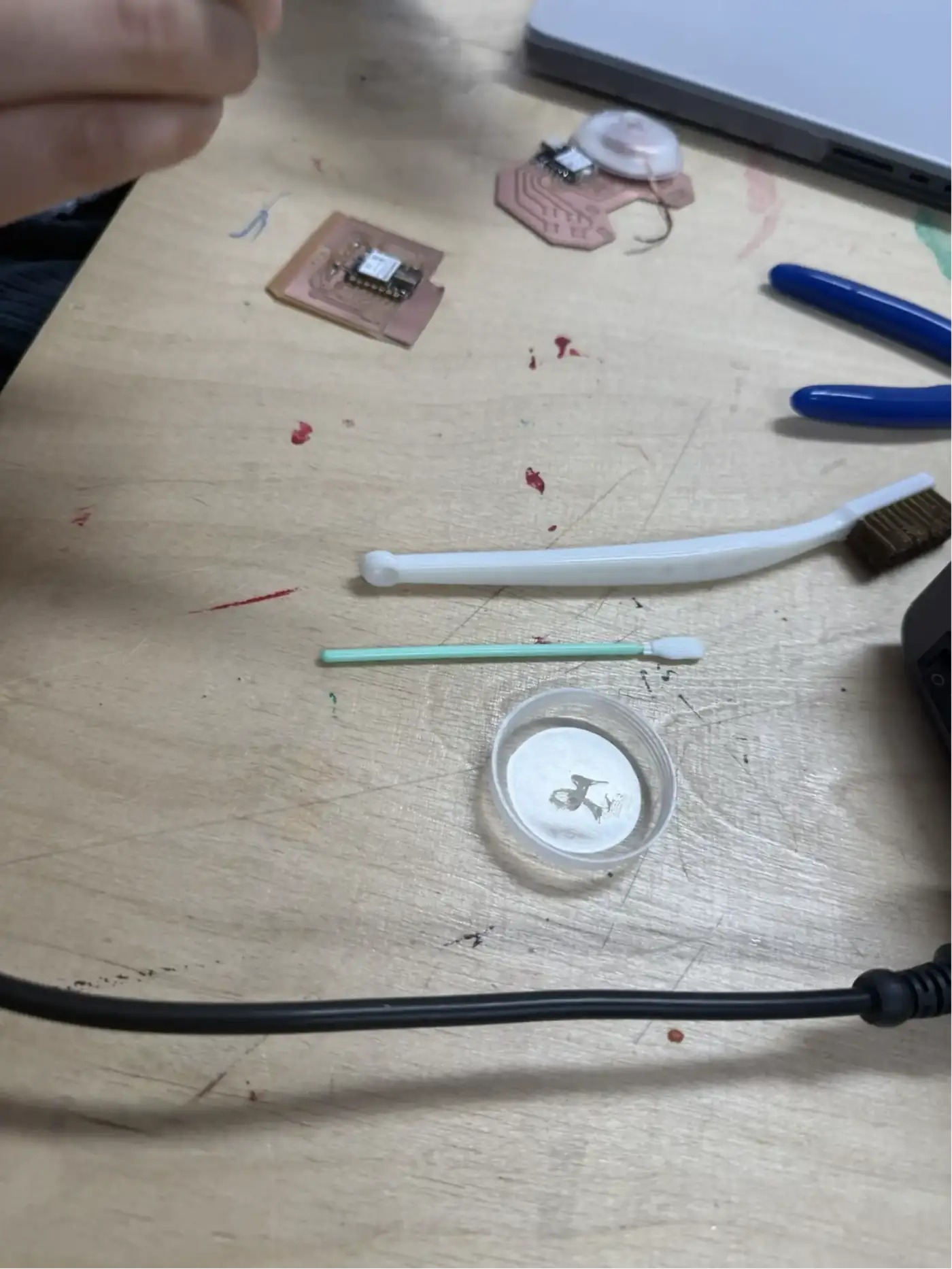
Cleaning the Milled Board
After milling, the board is removed from the machine and the copper dust is cleaned off. A brass wire brush is used to scrub the surface under a drop of isopropyl alcohol (IPA) or flux. This removes the fine copper particles that can bridge traces and also prepares the pads for soldering by lightly abrading the surface oxide.

Soldering the Components
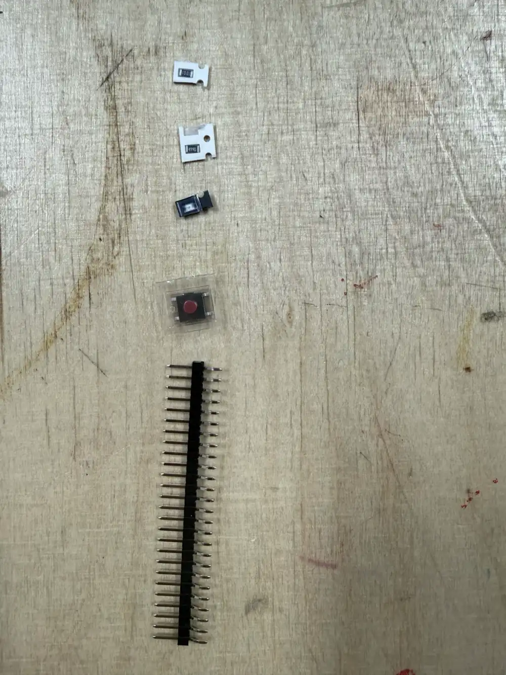
Components Used
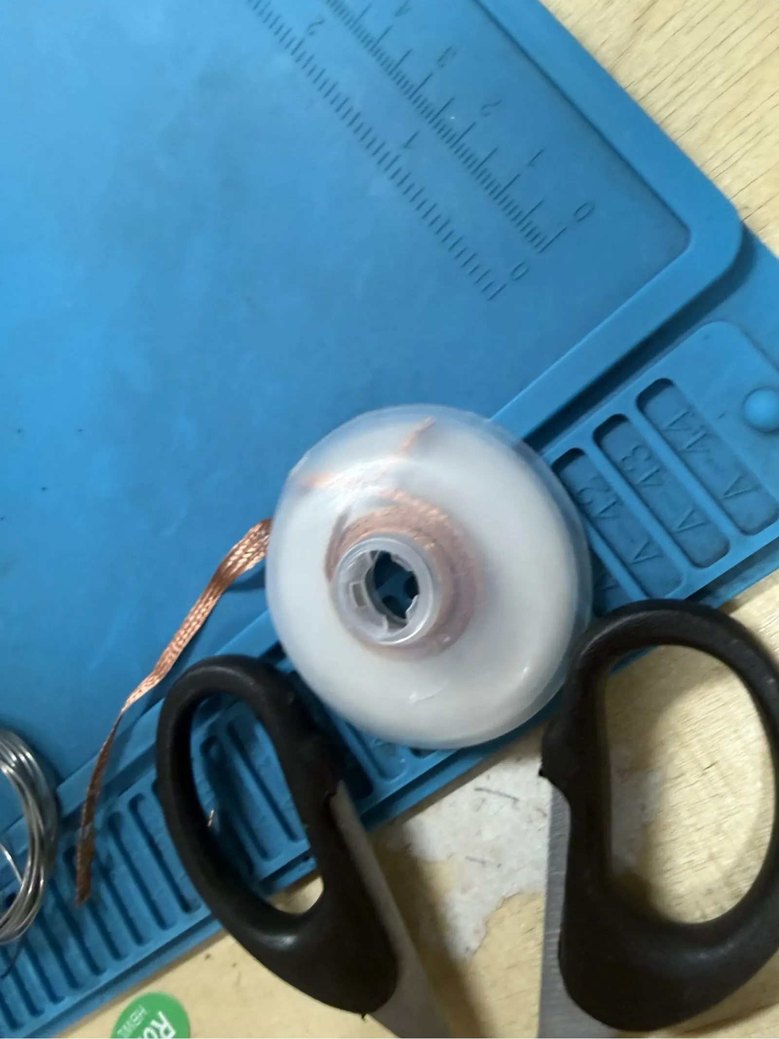
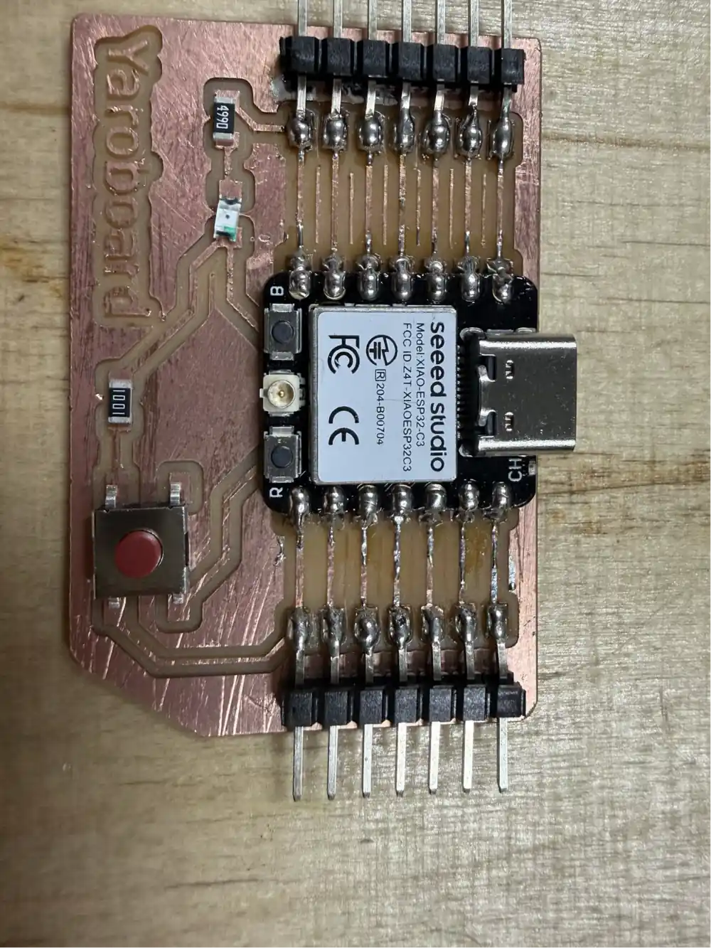
The Yaroboard is designed as a full breakout board for the Seeed Studio XIAO ESP32 C3 – a tiny USB-C microcontroller module with Wi-Fi and Bluetooth Low Energy. The component list is:
- Seeed Studio XIAO ESP32 C3 – the main microcontroller module (USB-C, dual-core 133 MHz, 264 kB RAM)
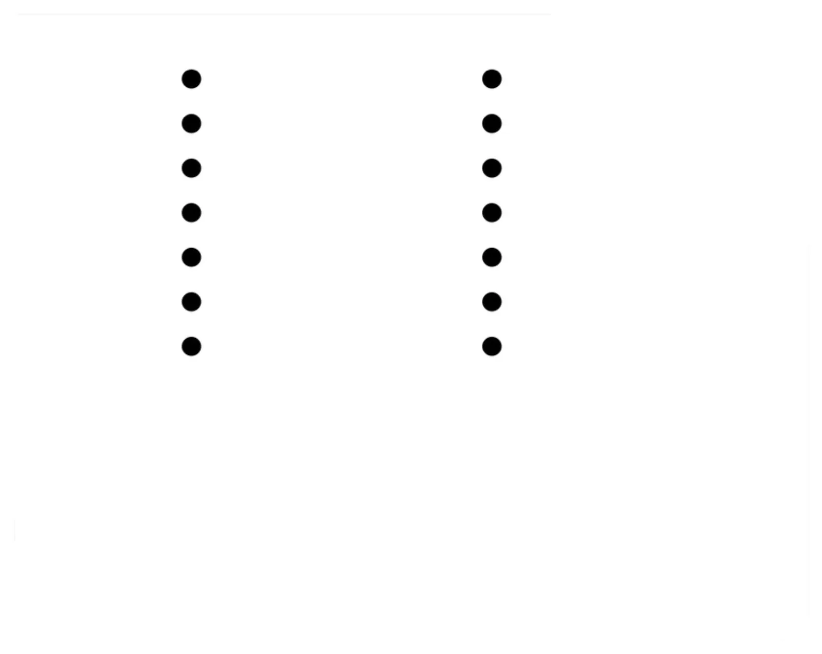
- 2 × 1×8 pin headers – GPIO access on both sides of the XIAO module
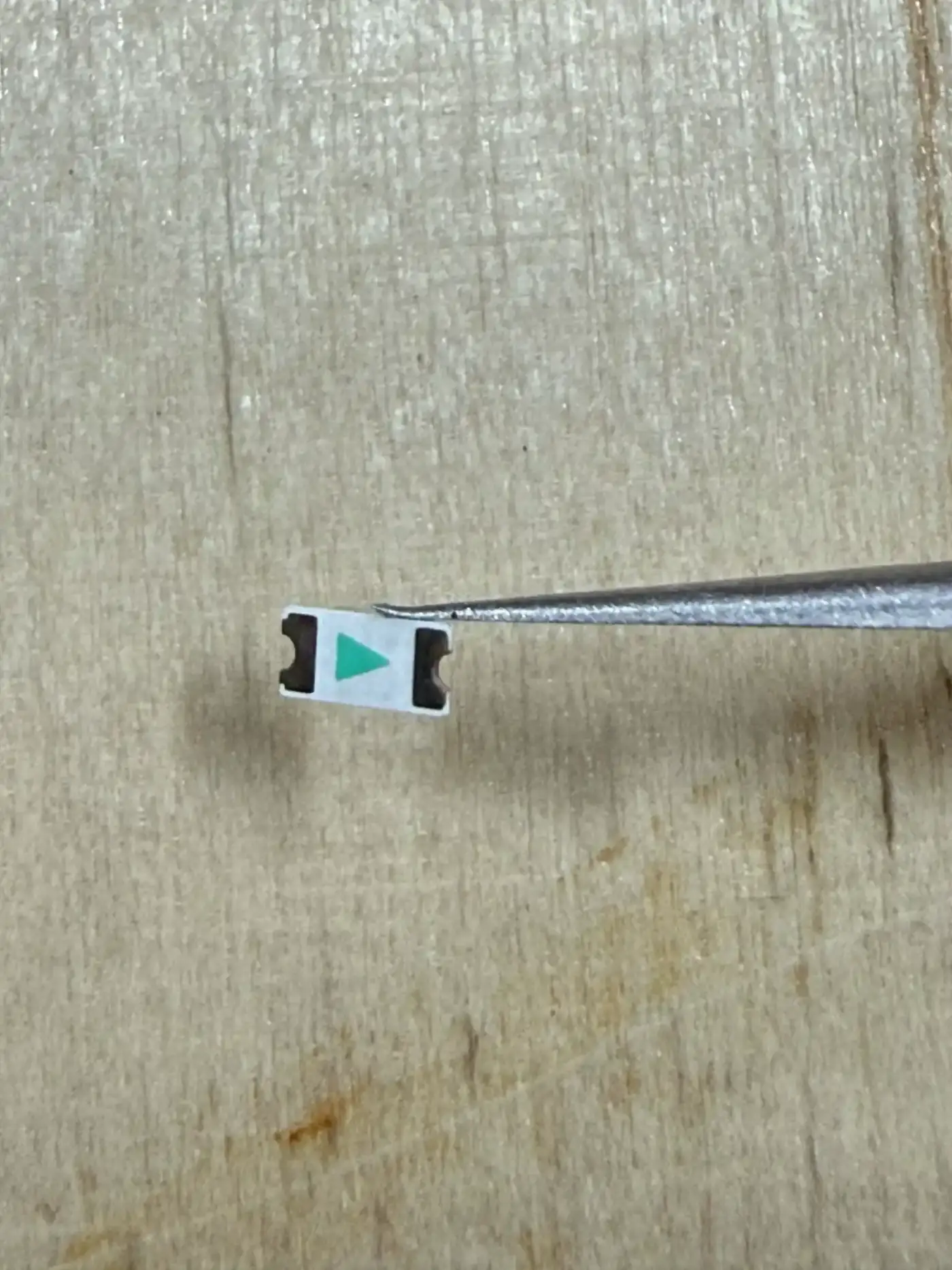
- 1 × tactile push button (SMD) – used as a reset or user-input button
- SMD resistors / capacitors – passive filter and pull-up components
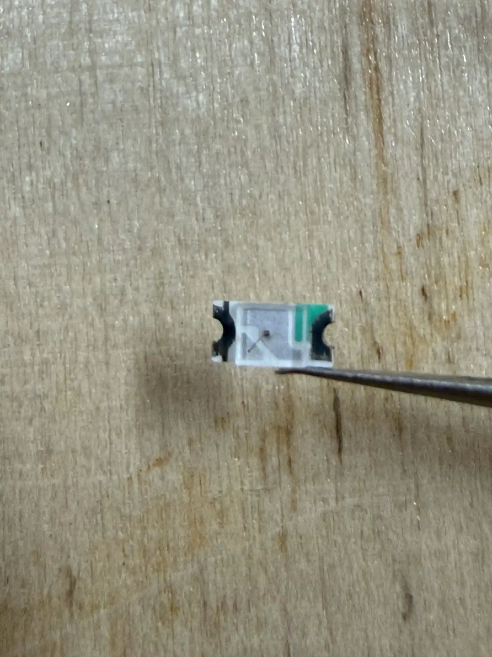
- 1 × SMD LED – status indicator
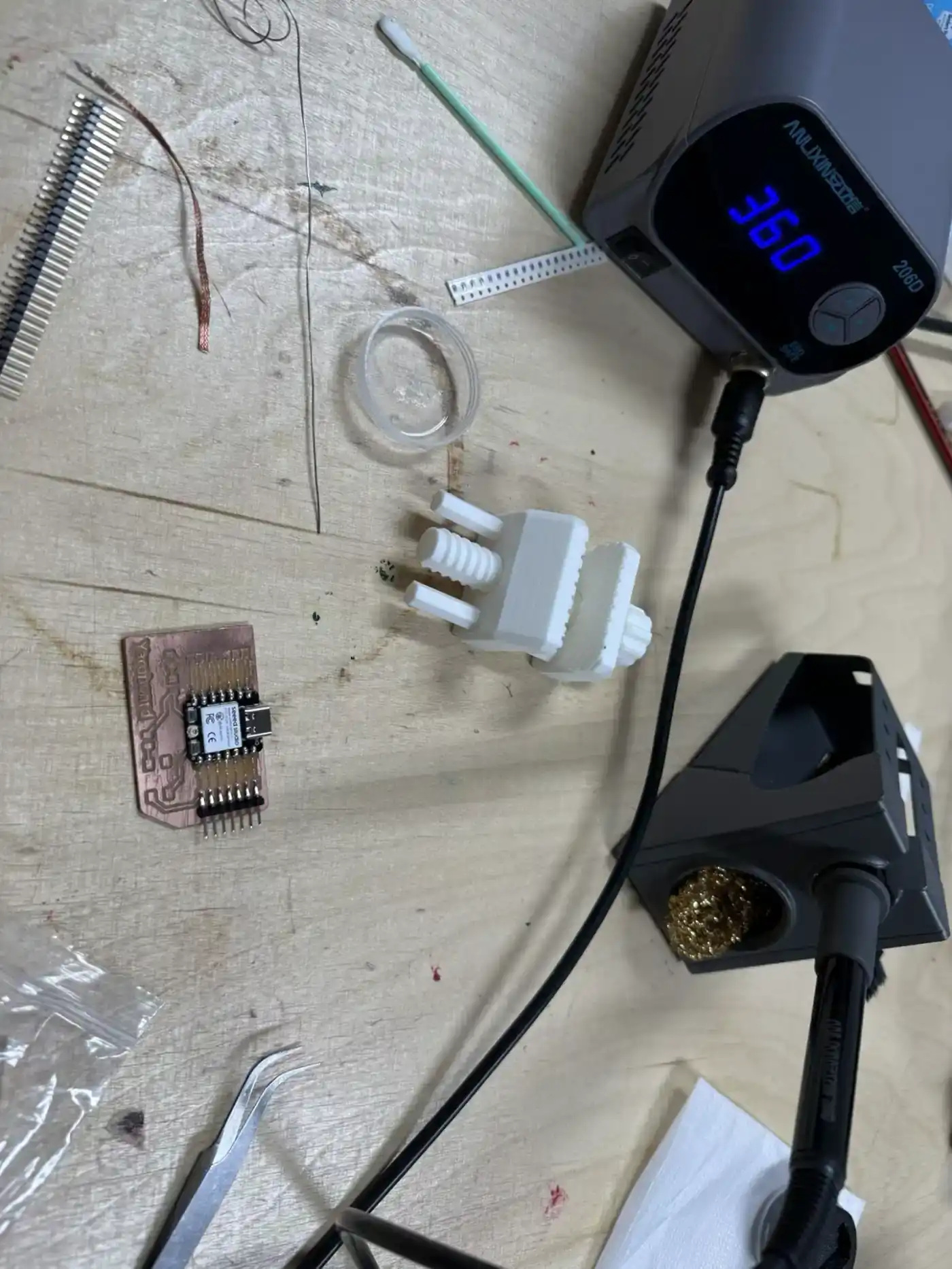
Soldering Setup
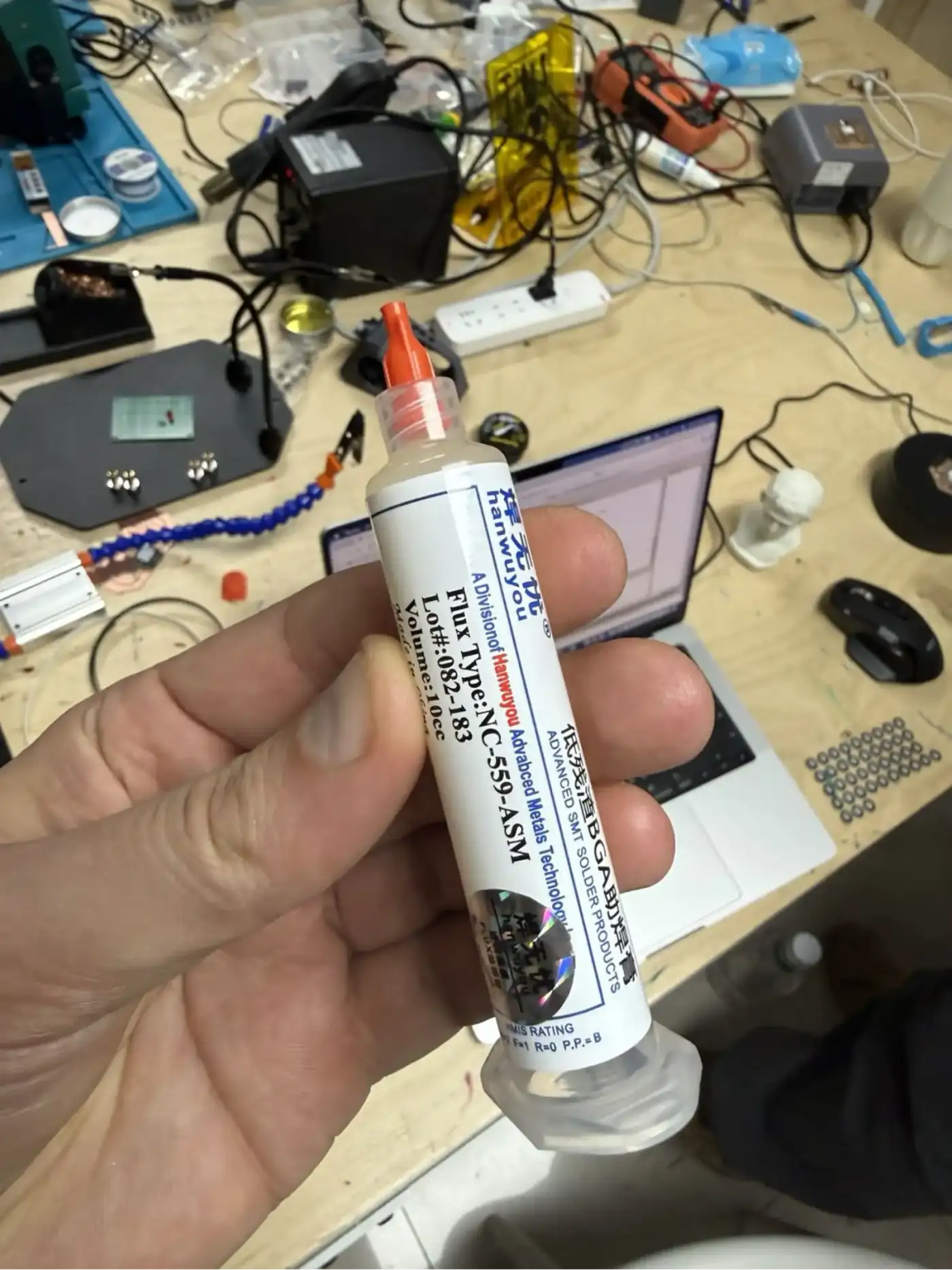
Soldering is performed at 360°C using a temperature-controlled soldering station. Liquid flux is applied to all pads before soldering – flux chemically removes the thin oxide layer on copper, dramatically improving solder wetting and joint quality. Solder paste (in a syringe) is used for SMD components; conventional solder wire is used for through-hole headers.
Populating the Board
The XIAO ESP32 C3 module is the first component soldered onto the board – it goes in the centre and sets the reference position for all other components. Pin headers are then soldered on both sides to expose all GPIO pins. SMD passives are placed using tweezers and soldered one pad at a time. The tactile button is soldered last.
After soldering, each joint is inspected visually: a good solder joint is shiny, smooth, and concave. A cold or dry joint appears dull and lumpy. Any solder bridges between adjacent pads must be removed with desoldering wick.
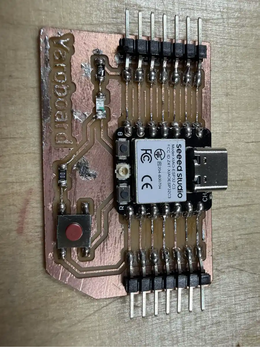
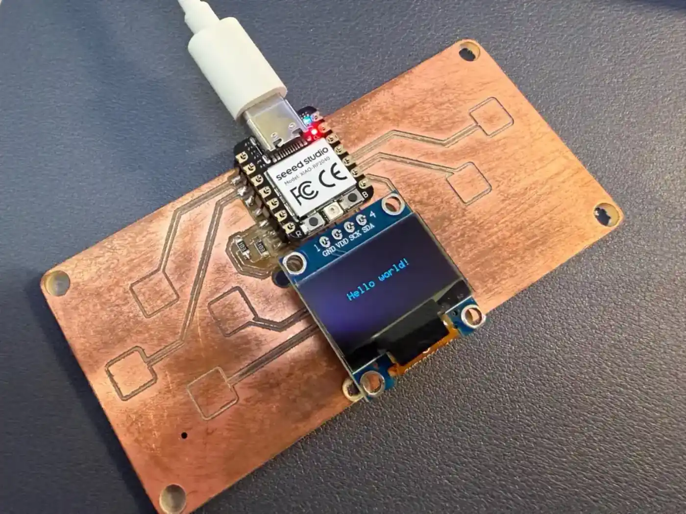
The Completed Yaroboard
The finished Yaroboard provides full GPIO access to the XIAO ESP32 C3 's 11 digital I/O pins, plus power and ground rails, through standard 2.54 mm pin headers on both sides of the board. The USB-C port of the XIAO module remains fully accessible for programming and power. An LED indicator shows power status, and the tactile button provides a convenient reset/user input without external wiring.
The board is ready to be programmed with CircuitPython or MicroPython via the USB-C port. It can be plugged into a breadboard or mounted directly into a project enclosure.
Testing the Yaroboard with an LED Output
After soldering the board, I tested that it could be programmed and that one of the GPIO pins worked as an output. For this simple validation, I uploaded an Arduino sketch that turns on an LED connected to pin D6. This test confirms more than only USB power: the microcontroller receives code, the pin header/output connection works, and the LED circuit can be controlled by software.
Code
void setup() {          // the setup function runs once when you press reset or power the board
  pinMode(D6, OUTPUT);   // initialize digital pin D6 as an output.
}

// the loop function runs over and over again forever
void loop() {
  digitalWrite(D6, HIGH);  // turn the LED on
}
Result
- The Yaroboard was powered correctly.
- The XIAO ESP32 C3 was programmed successfully through USB-C.
- The LED connected to
D6turned on, confirming that the board output works.
Conclusion: the board is functioning and working. The uploaded code controlled the LED from the microcontroller, so the milled traces, soldered connections, USB programming, and output pin were validated.
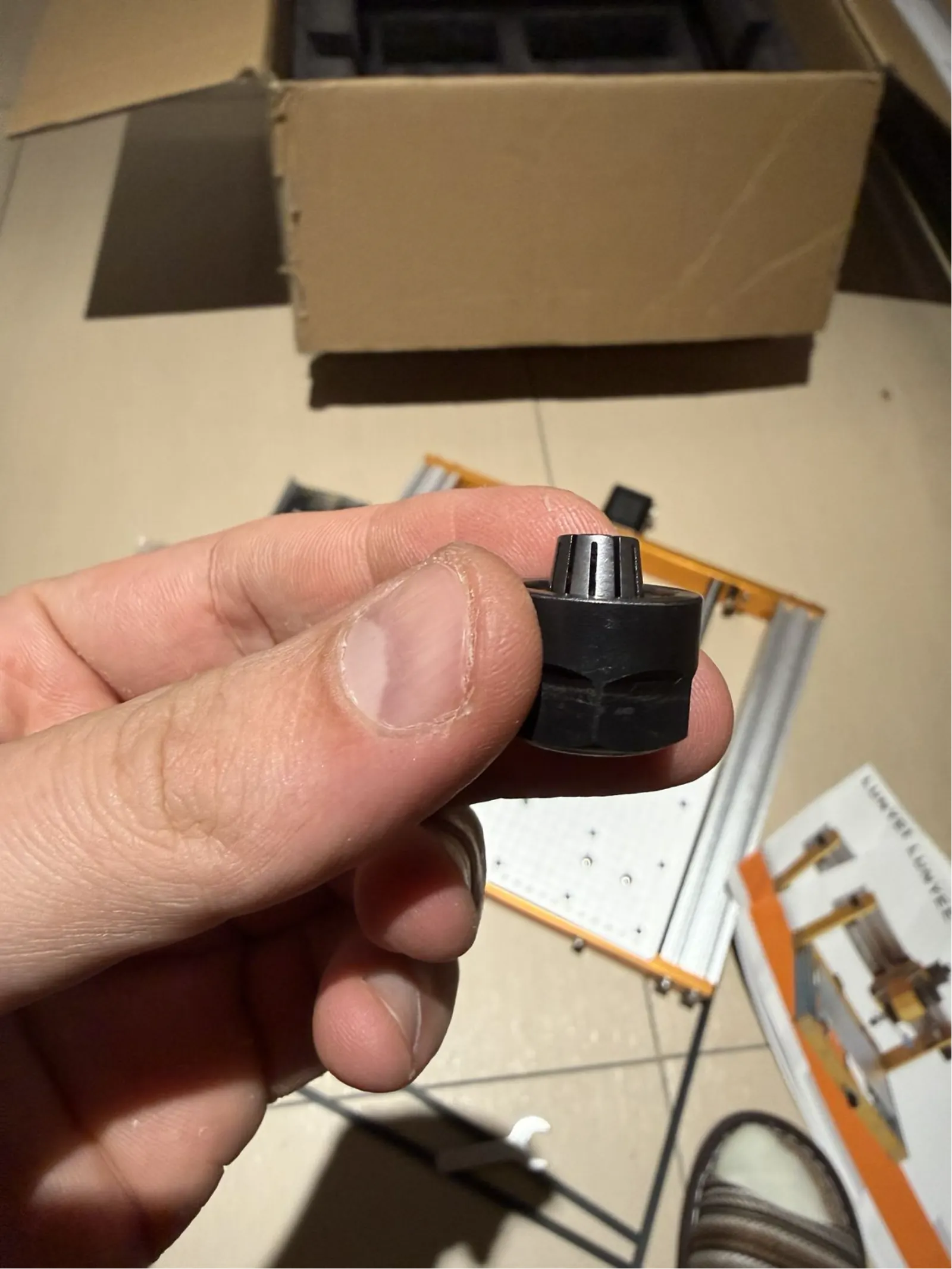
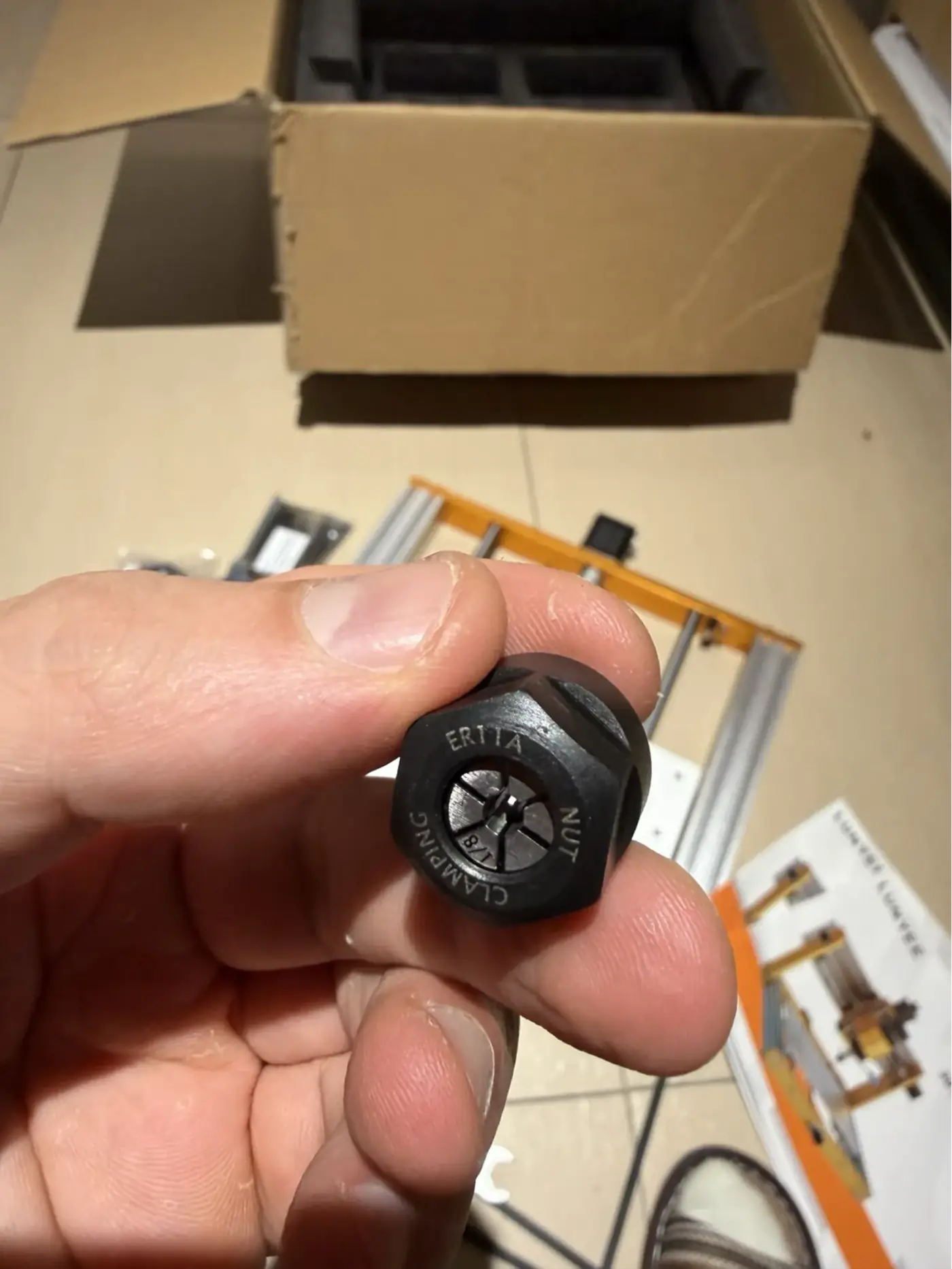
Assembling a Personal Desktop CNC Router Lunyee 3018
In parallel with the Fab Lab work, a small desktop CNC router kit was assembled at home during this week. This machine – a hobby-grade 3-axis CNC kit – is intended for light-duty PCB milling, small engraving jobs, and general experimentation. It runs on a GRBL controller (the same G-code sender used in the Candle software shown earlier).
Building and commissioning your own CNC machine is an excellent way to deeply understand how these machines work mechanically and electronically – stepper motor drivers, limit switches, work coordinate systems, and feed rate tuning all become hands-on learning.
Preparing the Copper-Clad Board
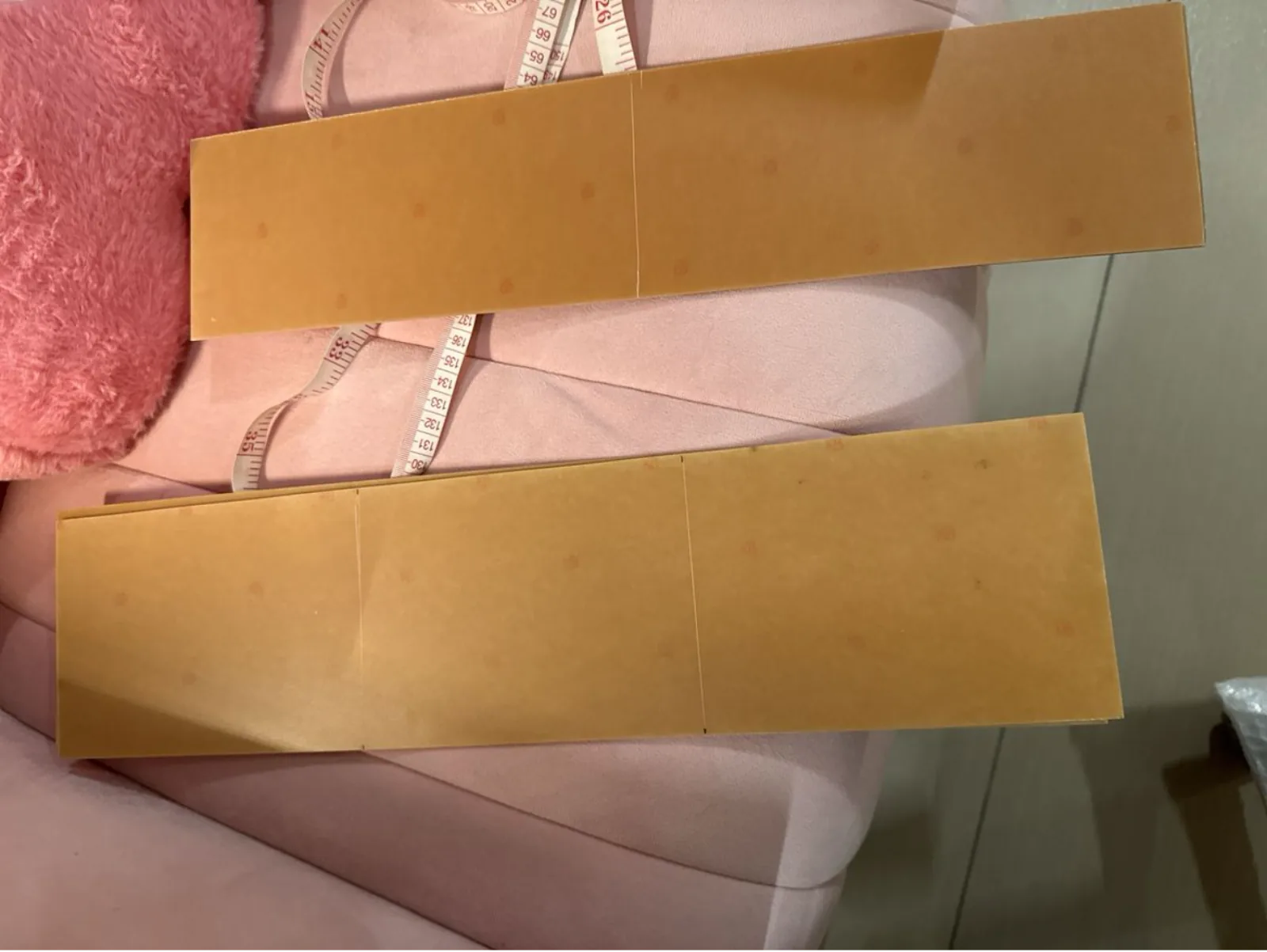
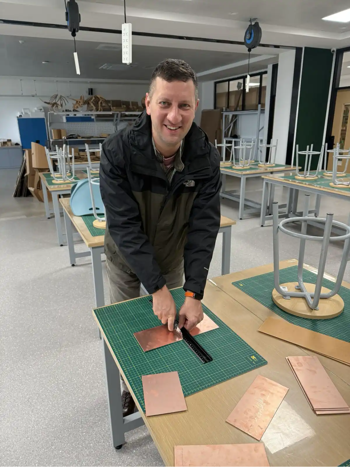
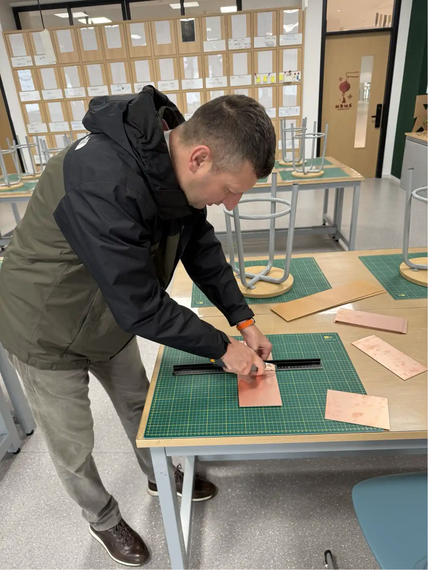
The raw material for PCB milling is an FR1 (or FR4) copper-clad board – a rigid substrate coated with a thin copper layer (typically 35 µm / 1 oz). Before loading it into the machine, the board must be cut to a size that fits the job and the machine bed.
A steel ruler and utility knife are used on a self-healing cutting mat. The technique is to score the board firmly three or four times along a ruler edge, then snap the board cleanly along the score line. This gives a clean, square edge without dust or cracking.
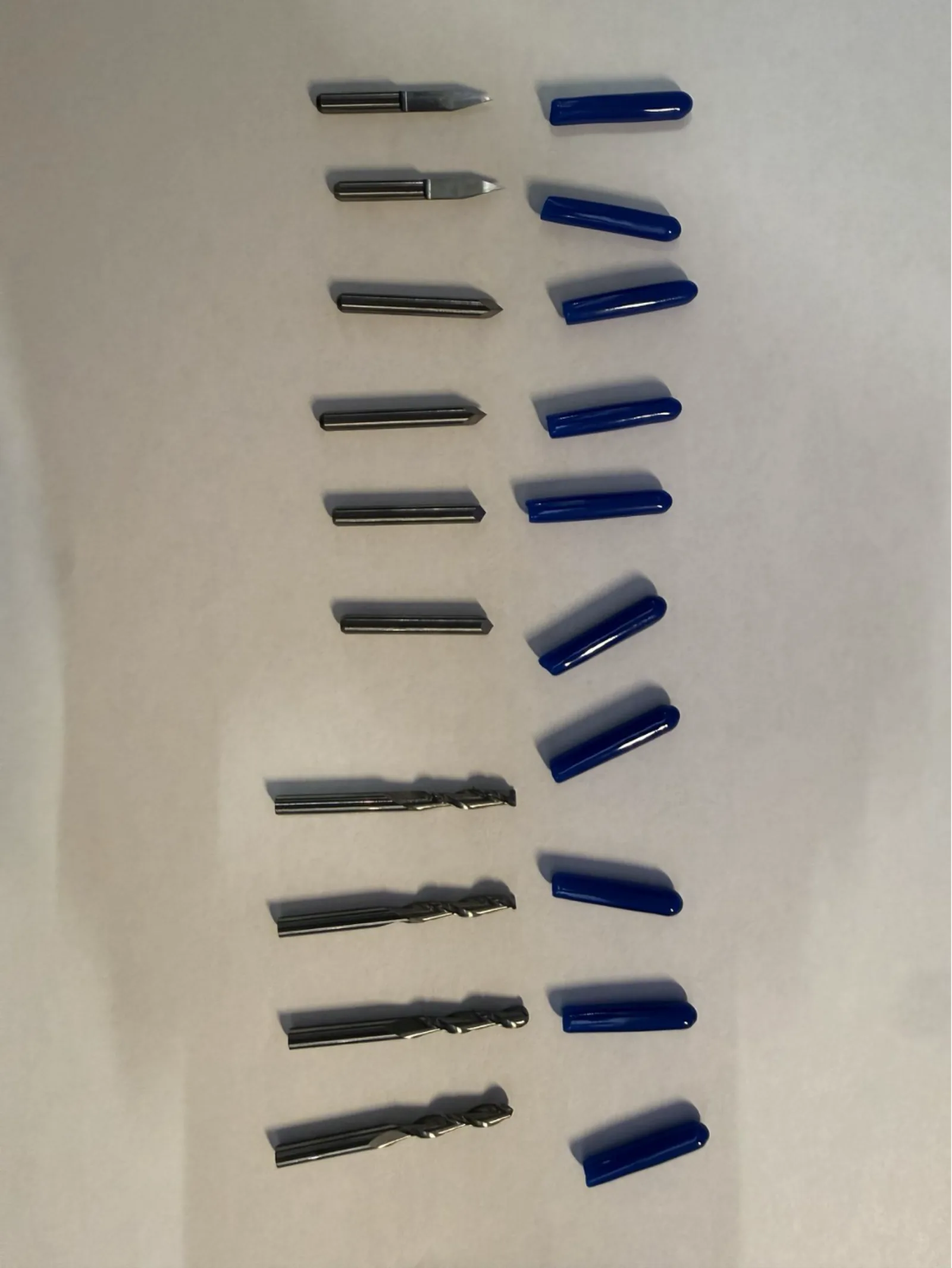
Engraving Bits and End Mills
PCB milling uses two different categories of cutting tool:
- V-bit engraving bits – a sharp-tipped bit with a V-shaped profile. Used to mill isolation channels between copper traces. The cut width depends on the bit angle and the depth of cut: shallower depth = narrower trace channel.
- Spiral end mills – standard CNC router bits with 1–2 flutes. Used for the board outline (profile) cut, drilling holes, and any wide copper removal areas.
It is important to select the correct bit for each operation and to inspect bits before use for any damage or dullness. A broken or chipped bit will ruin the copper traces.
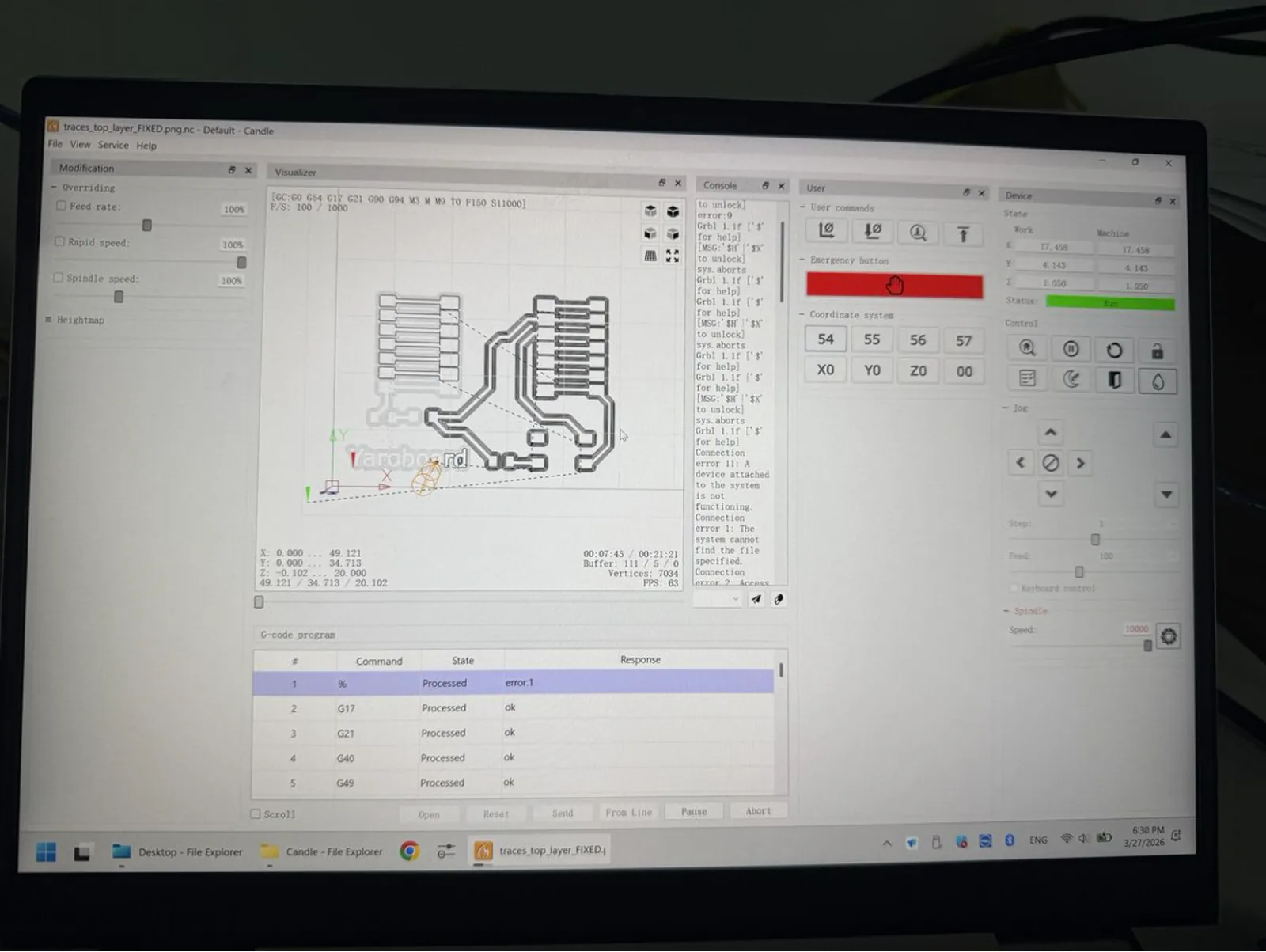
Lunyee 3018 Milling
This time, for milling traces, I wanted to try a V-bit on the Lunyee 3018 CNC machine. I installed it in the spindle and started the milling workflow using Candle, the GRBL sender software recommended by the machine supplier. Candle is beginner-friendly and makes it easy to load the toolpath, set the work origin, and send the job to the machine.
For the outline cut, I used a larger ball end mill. It worked well for releasing the board from the stock, although for smaller details and holes a smaller end mill would be better.
After soldering my second Yaroboard, it worked the same as the first one and was ready for the next operations.
QPad PCB
As recommended, I decided to mill one more board: the QPad PCB for experiments. I found the Gerber files and assembly information on Quentin Bolsee's GitLab page:
https://gitlab.cba.mit.edu/quentinbolsee/qpad-xiao
I also had a XIAO RP2040, so I made one more board for that microcontroller and prepared the electronic components for assembly.
At that time I did not have a small enough end mill to drill the 1 mm holes, so I used a drill press and drilled them manually. This allowed me to install pin headers and remove the microcontroller module when needed, without soldering the microcontroller permanently to the board.
I also received a display and the necessary components for the QPad with the XIAO RP2040, then uploaded test code from Quentin's page.
I tried the Tetris game and it worked well. Based on that test, I asked ChatGPT to help write another game in the style of Space Invaders, with simple graphics and animation.
QPad display test code from Quentin's repository
Create a beginner-friendly Space Invaders style game for an Arduino Uno with a 128x64 I2C OLED display and push buttons.

Hardware setup:
- Board: Arduino Uno
- Display: SSD1306 128x64 OLED display, I2C
- OLED VCC -> 5V
- OLED GND -> GND
- OLED SDA -> A4
- OLED SCL -> A5
- Left button -> D2
- Right button -> D3
- Shoot button -> D6
- Each button uses INPUT_PULLUP
- One side of each button goes to the Arduino pin
- The other side of each button goes to GND
- Optional: buzzer on D9 for simple sound effects

Game request:
Generate a simple Space Invaders style game where the player controls a spaceship at the bottom of the OLED screen, moves left and right, and shoots upward at enemy invaders. The enemies should move across the screen and slowly come downward. The game should include a start screen, score display, simple enemy animation, collision detection, game over screen, and restart option. Please provide complete Arduino Uno code ready to upload, list the libraries needed, explain how the controls work, and briefly explain the main functions of the code in simple language so students can understand and learn from it.
After some tuning and customization of the interface, I could play the game. It has three levels and difficulty progression, which made this a fun extension of the electronics production assignment.
Reflection
This week I learned the full workflow of making a PCB: preparing files, generating toolpaths, milling traces, cutting the outline, soldering components, and testing the final board. It helped me understand that PCB production is not only a digital process; small physical details like bit choice, Z-origin, board flatness, and milling depth can strongly affect the result.
One important highlight was using a V-bit on the Lunyee 3018 CNC machine. The traces came out very clean, and the board needed less cleaning after milling. I also learned that tool selection is very important. My outline bit was a little too large, and I did not have a small end mill for 1 mm holes, so I solved this by drilling the holes manually with a drill press.
I successfully made and tested my second Yaroboard, and it worked the same as the first one. I also milled a QPad PCB for the XIAO RP2040, soldered the components, connected the OLED display, and tested it with example code. Running the Tetris game and then creating a Space Invaders style game with AI support was an exciting extension of the assignment.
For next time, I want to prepare better tools in advance, especially smaller end mills for drilling and outlines. Overall, this week helped me become more confident in PCB production and showed me how design, milling, soldering, and programming all connect together in one complete workflow.
References
- Fab Academy reference (Quentin Bolsee)
- Gerber to PNG converter (FabLab Kerala)
- Namita Aravind - Week 8 documentation
- Yaroboard EasyEDA production project (.epro)
- Yaroboard Gerber archive
- Yaroboard traces RML for Roland milling
- Yaroboard outline RML for Roland milling
- QPad Space Invaders Arduino source code