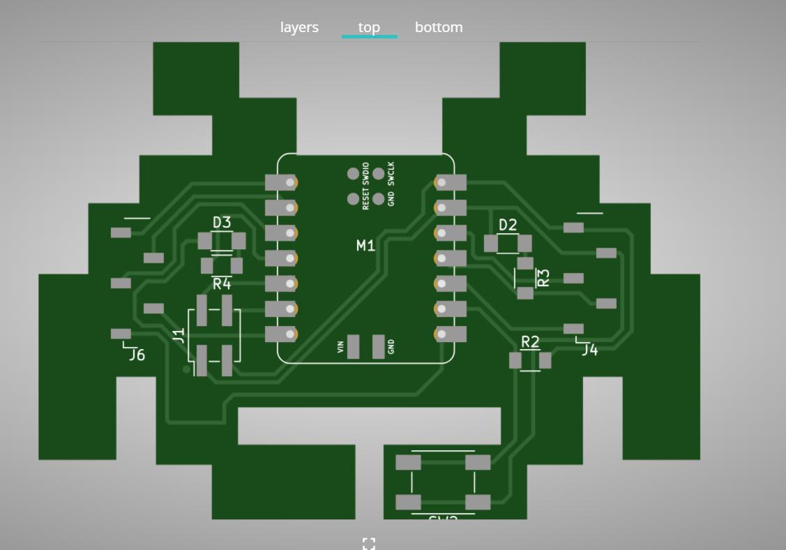
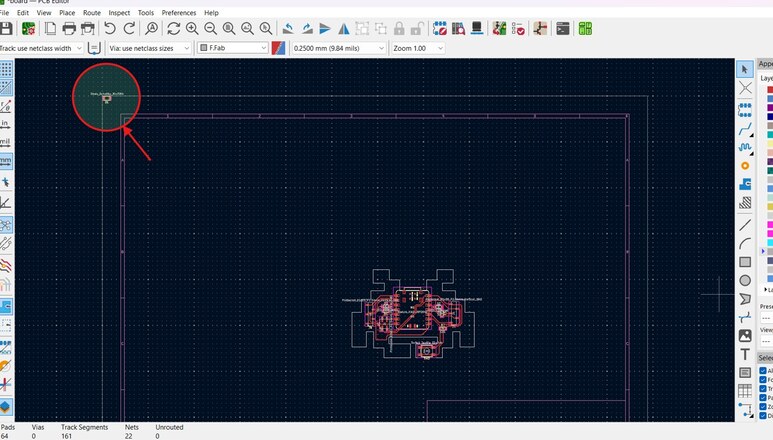
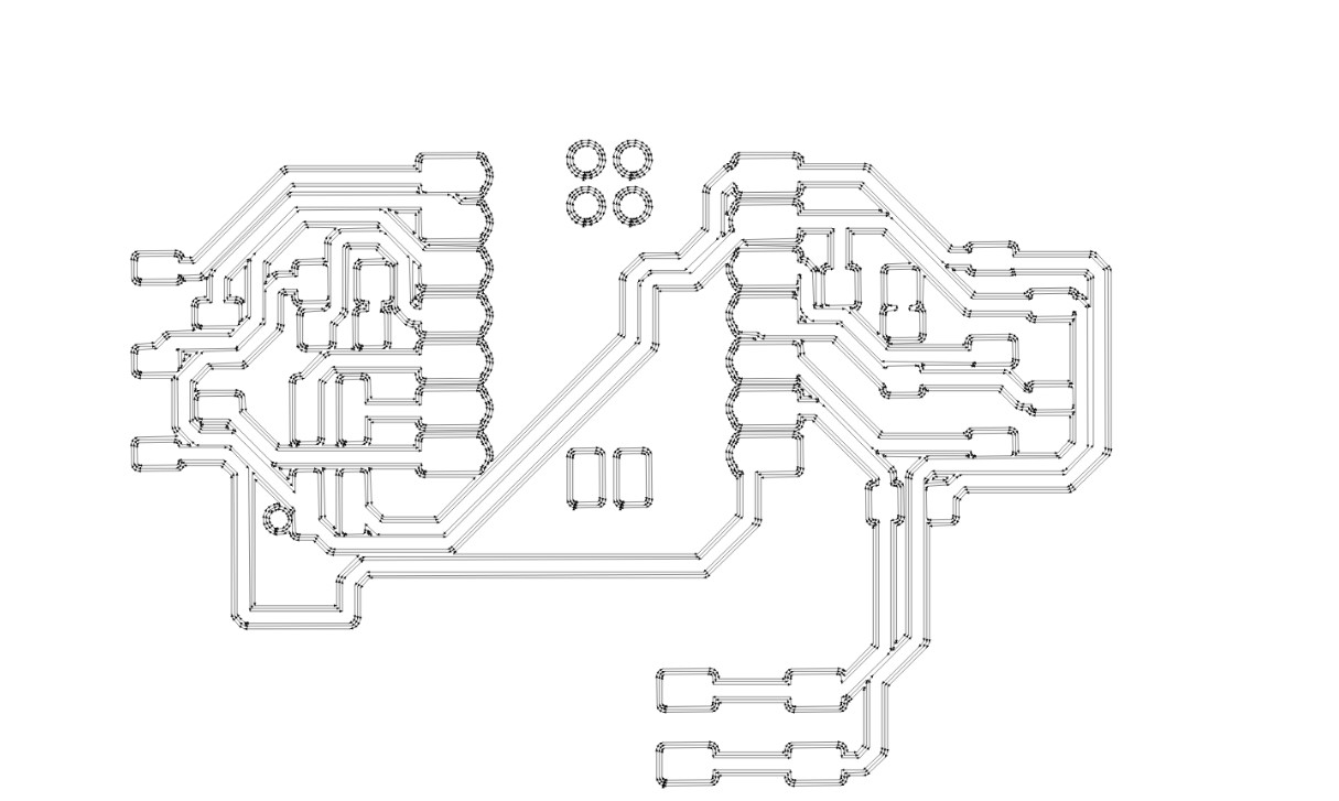
I would be making the space invader PCB that i designed during Week06 where we did electronics designing.
I cross verified the board and checked the dimensions of the design which turned out to be 48 x 66.3cm.
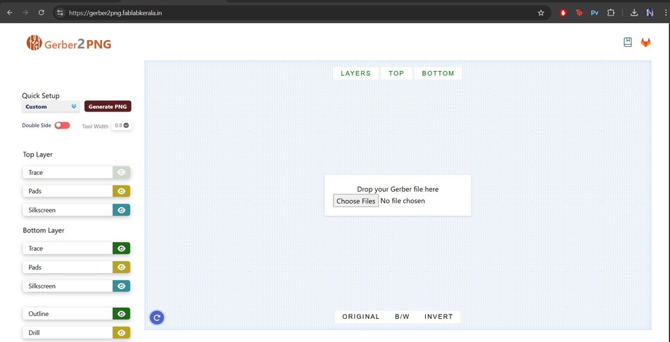
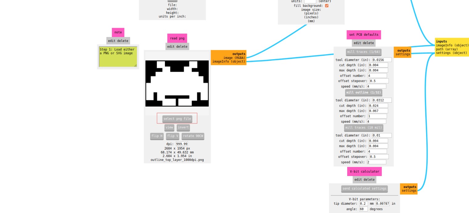
Gerber To Pngs
First thing I did was to convert the gerber files into pngs that will feed the
traces and outlines to the machine.Gerber2png was the website we
used to easily convert the files. It is a website that was developed in
Super Fablalab, Kerala to facilitate this process.
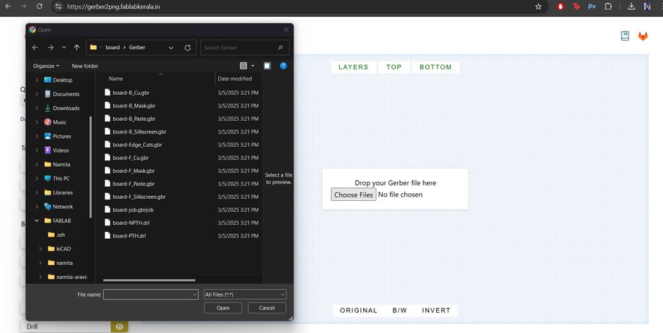
Drop the gerber files on the site
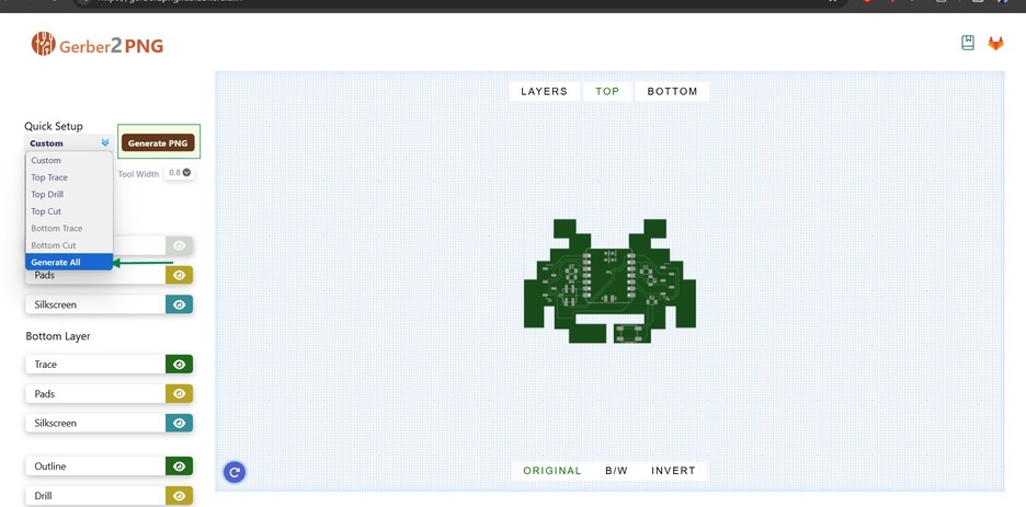
On the quick set up drop down choose 'Generate all'. Then click Generate PNG
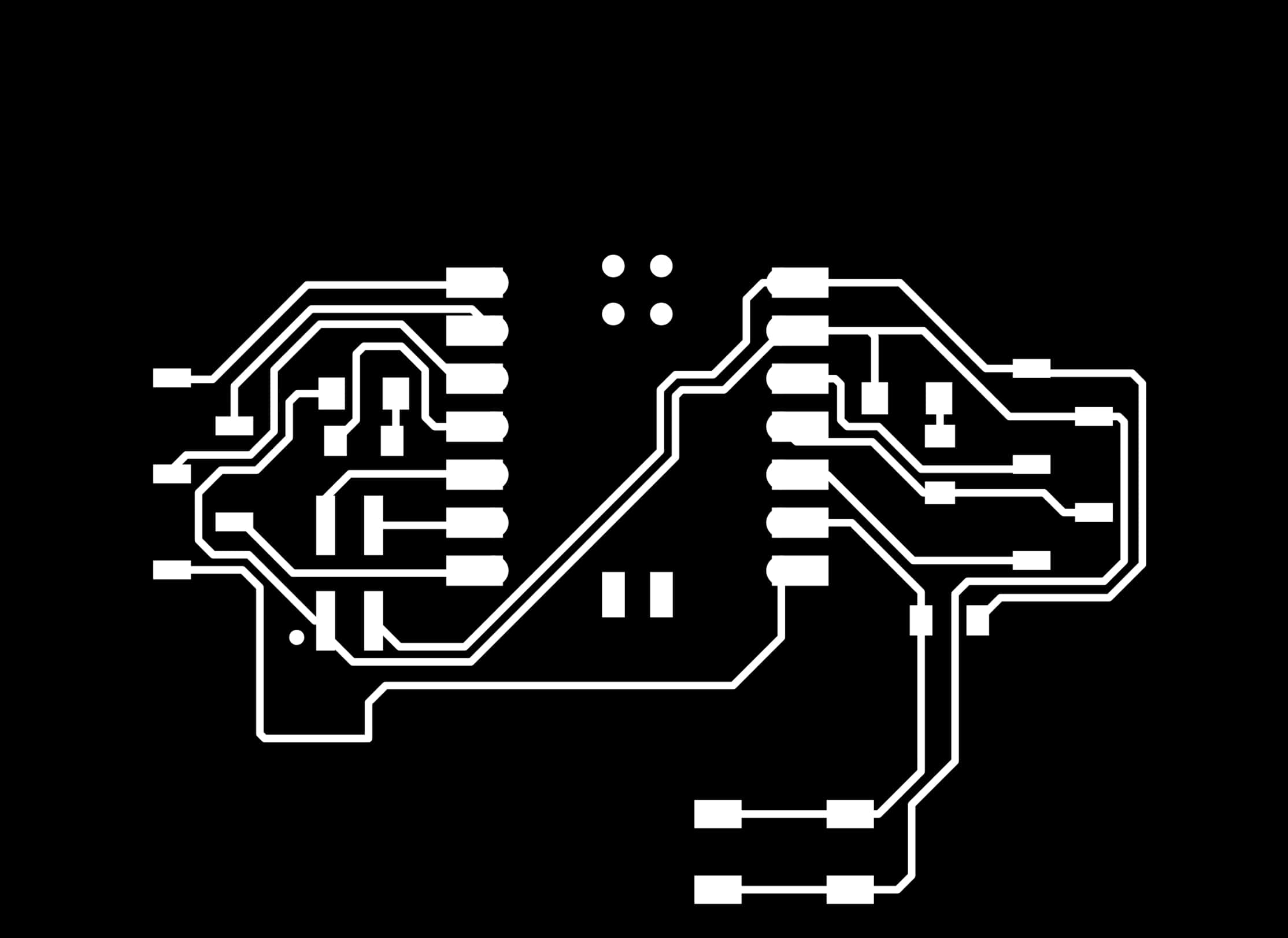
The png of the traces, outlines and drill holes(if any) will be generated
Download the files to upload into the mods software.
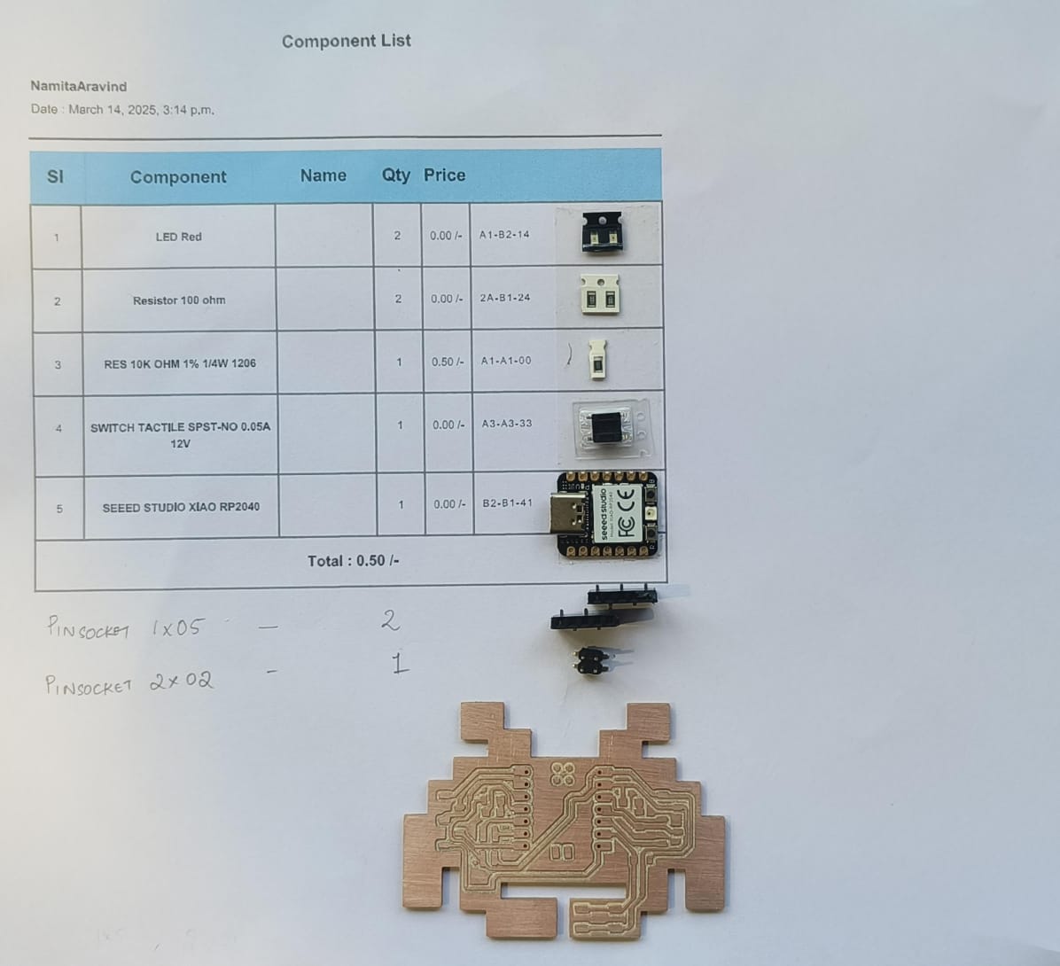
Gathering the components from the inventory
We have to collect the components required for our PCB and prepare a BOM for it.
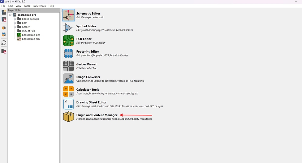
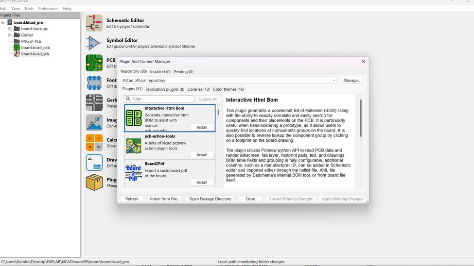
We can obtain the BOM from the PCB easily from a KiCAD plugin. To load the plugin click on Plug ina nd
content manager.
Then install the Interactive Html BOM plugin
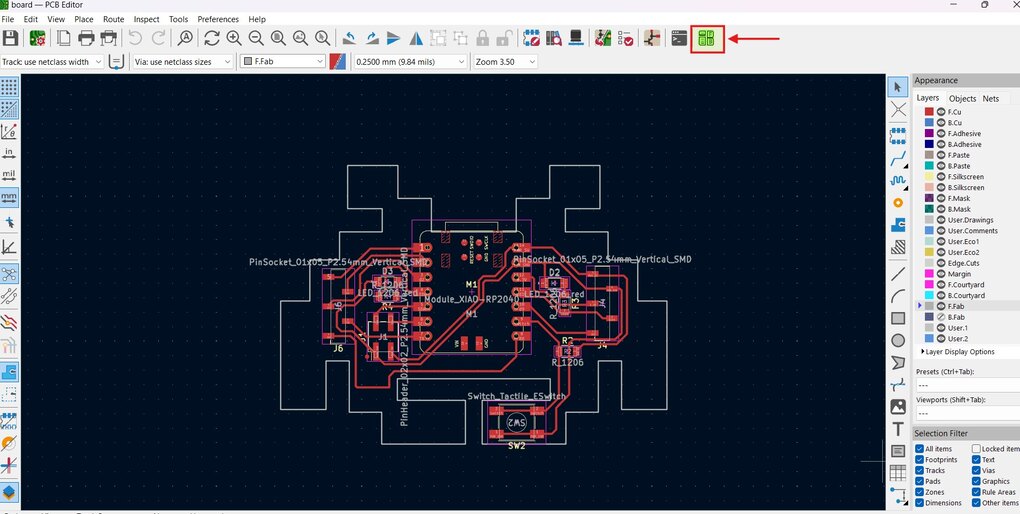
Now we can go to the PCB editor window and click on the plugin we just installed from he ribbon.
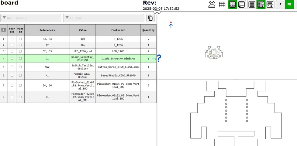
You will get directed to a page where the BOM is displayed along with the pcb with components.
When you hover your mouse over the component on the table U shall see the corresponding part highlighted.
I noticed that a random diode appeard on my list that wasnt present on my PCB. I could not understand how it
happened
first but when my batchmate zoomed out the layout we noticed a diode component floating around far from the PCB.
So make sure to double check the list with the components on the PCB.
I fixed the issue by removing the unnecessary part and this was how the BOM looked like for my PCB.
This is the interactive BOM for my PCB
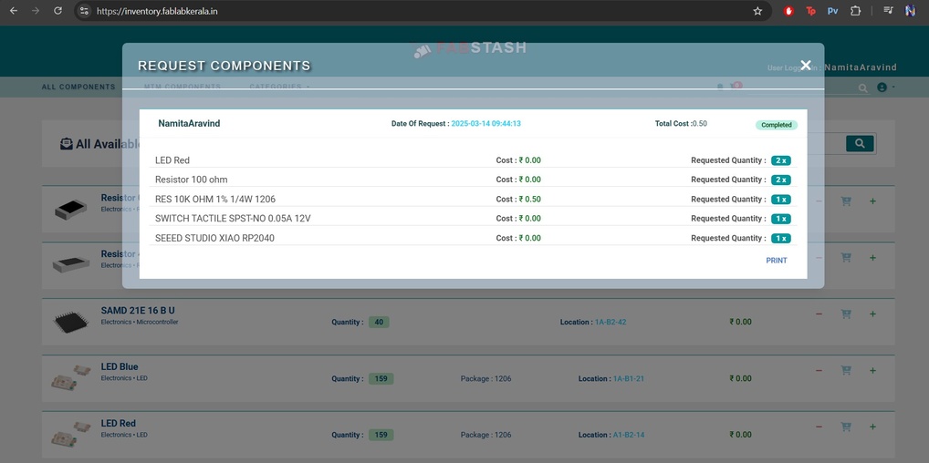
Now we have to check whether all the components that were required is available in our lab's inventory.
We were able to check this easily by using Fabstash website which shows the available stock of components in our
inventory and keep log of incoming and outgoing items.
We can add the parts we need to the cart and send a request to avail them.
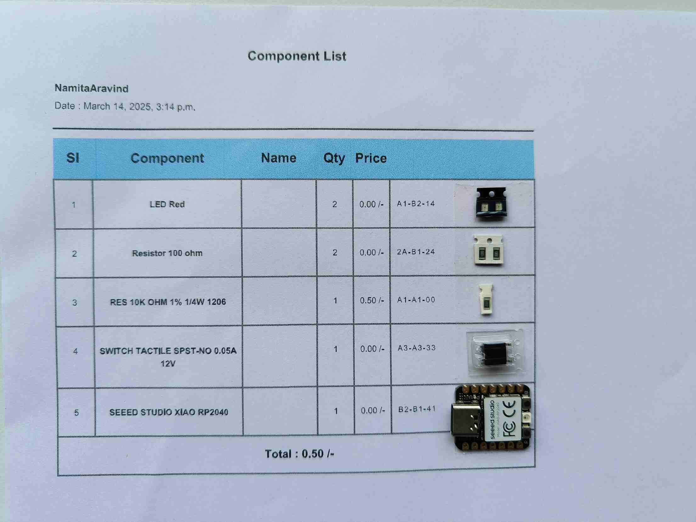
I printed out the form and went on to pick out the components i required and stuck them on to the paper to
easily keep everything in place.
There was some bug on the website that did not show the correct price of the components xD.
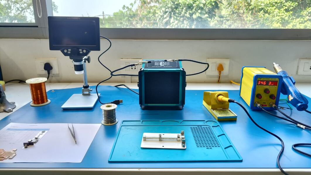
Placing the board to the bed
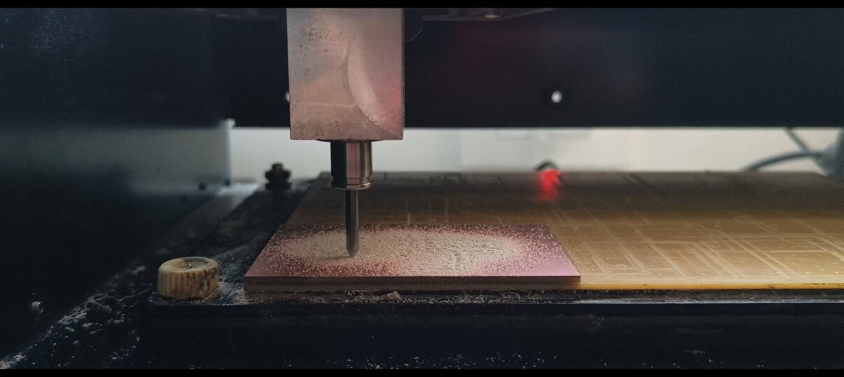
> I sanded the board to remove the oxidation layer . Then I fixed the PCB to the bed using double sided tape.
Position the PCB so that the edges line up with the bed edge.
We got a detailed explanation done by our instructor about the Modela MDX 20 milling machine, which we would be
using to cut out the PCB. This is documented in detail in our group assignment.
Fixing the tool to the machine
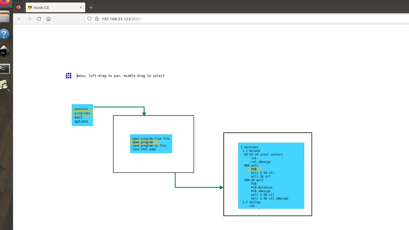
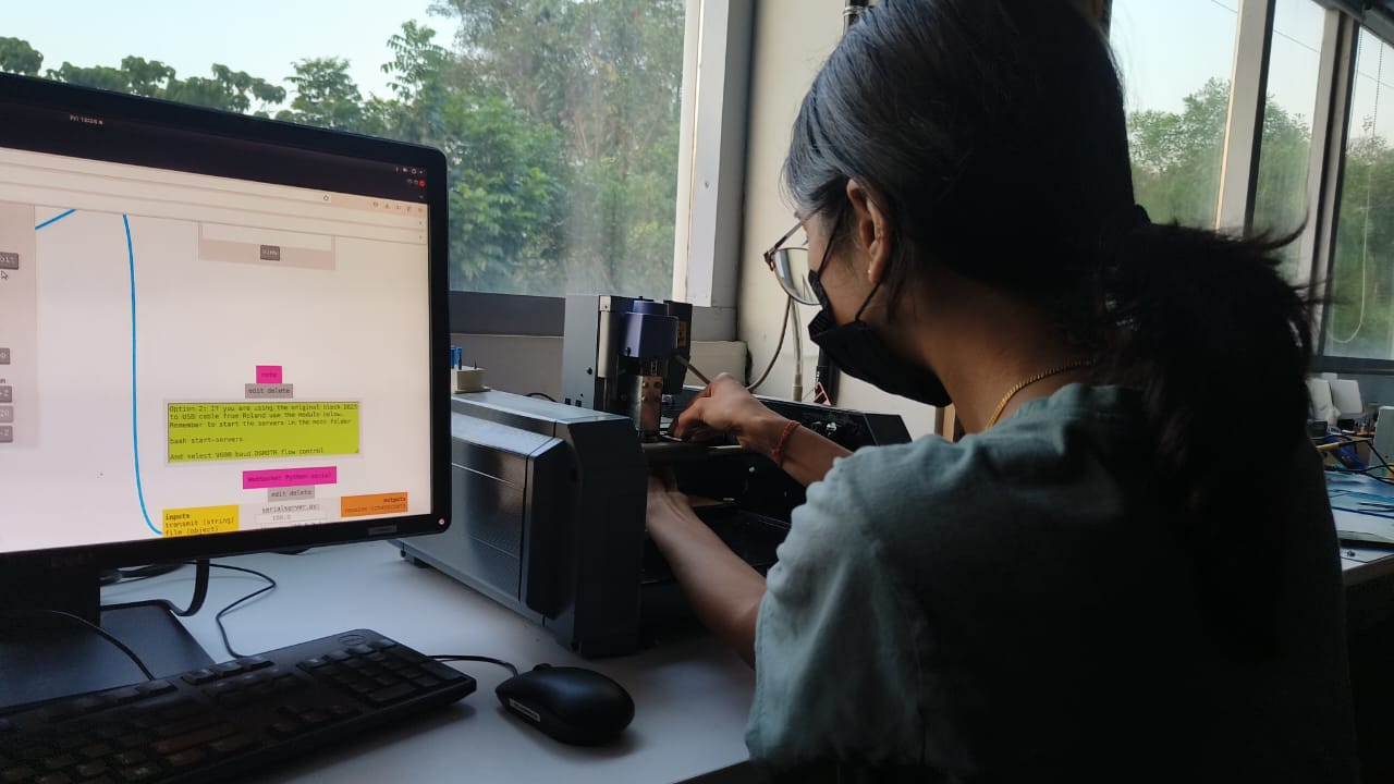
Open the MODS software:
We have to enter a series of commands related to the functioning of the machine.
We need the machine to do the traces in the beginning with a 0.2mm 60 degree V bit first , then we go on to do the
drilling
for the
holes and the outlines with a 1/32" flat endmill at the end.
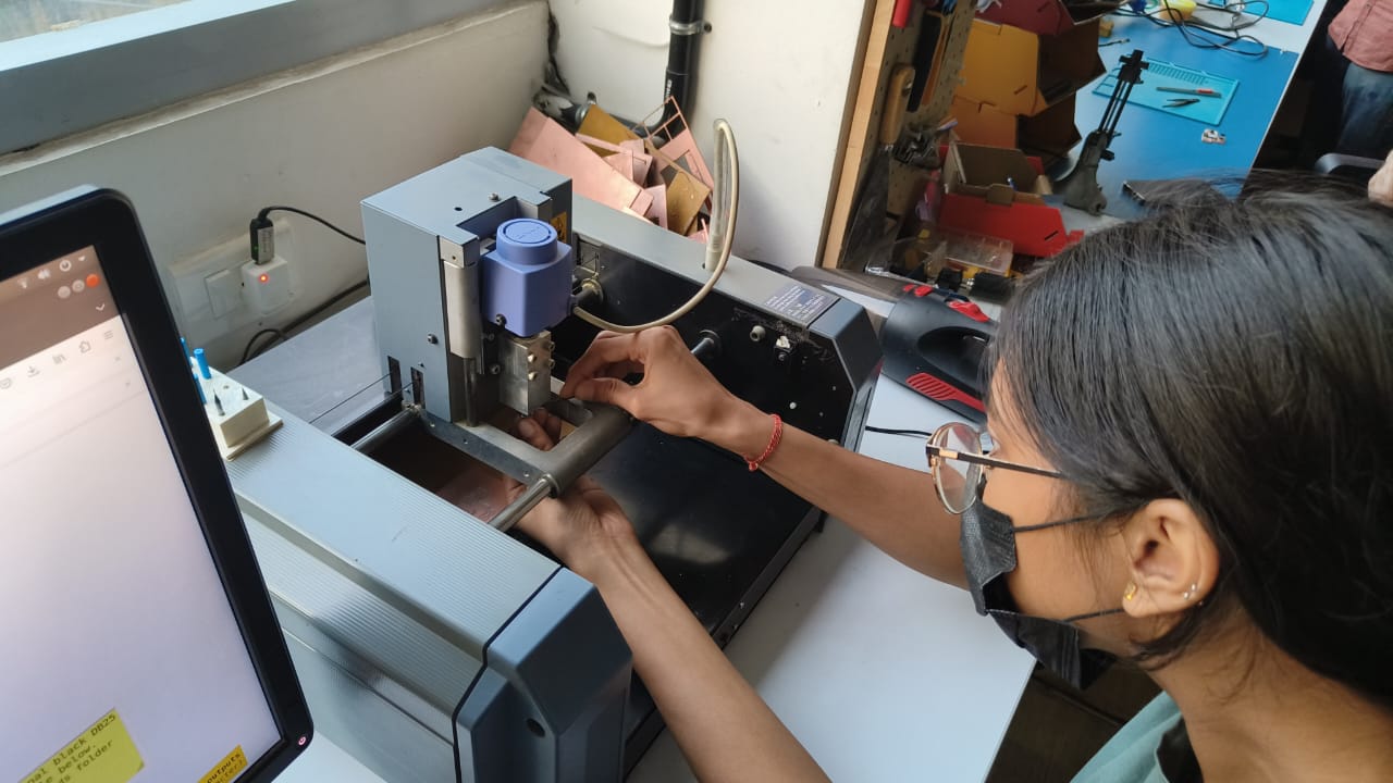
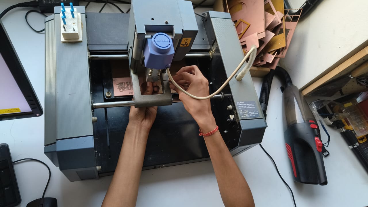
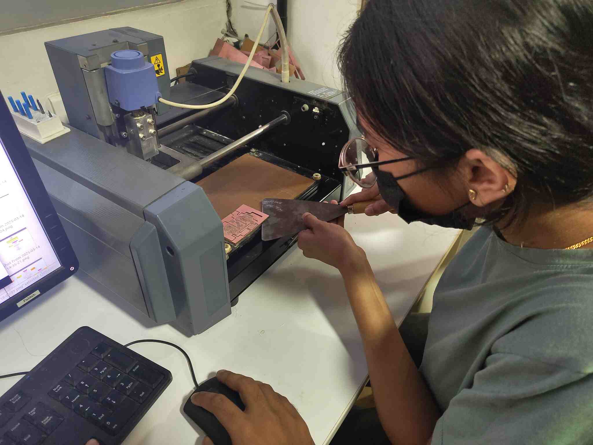
We need to fix the tool to the the spindle of the machine. We should be very careful while handling the bit
because it breaks off very easily.
So while placing and taking out the bit always be cautious of the bit not dropping suddenly.
Go to the mods software and then click on position to change bit. This has been set in our lab for the ease of
changing the the bit .
It is almost at the center of the machine so that our hands could easily maneuver the tool.
Now insert the tool into to the spindle and tighten just enough that the bit won't fall off.
Next we need to bring the tool on top of the PCB by giving values to x and y axis in the mods software.
Then we loosen the bit so that it drops lightly on the bed. Now tighten the bit very well.
This was process was done to find the z axis level.
We need to set our x and y axis now. For this we keep adjusting the values of the x and y offsets until we
reach the corner of the board.
Keep in mind the dimensions of ur PCB so save space and position it accordingly.
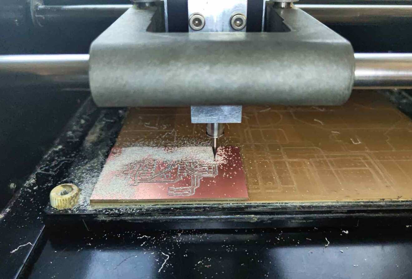
Now that we have set the levels of the machine we can start the process to do the traces.
Setting up the Software(Using MODS) and operating the machine.
To make traces.
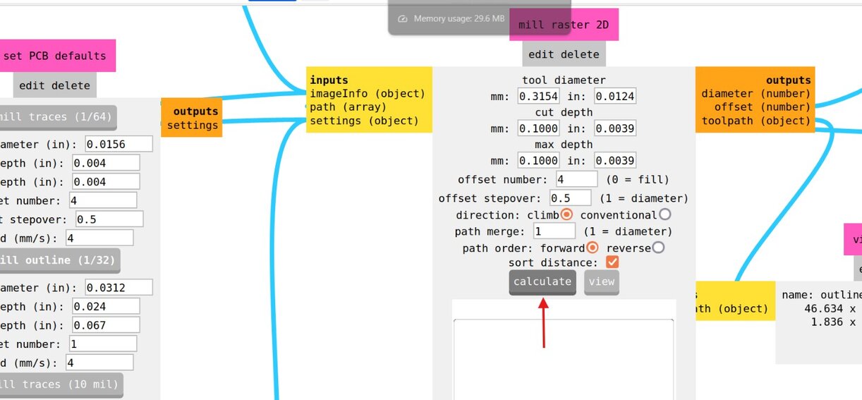
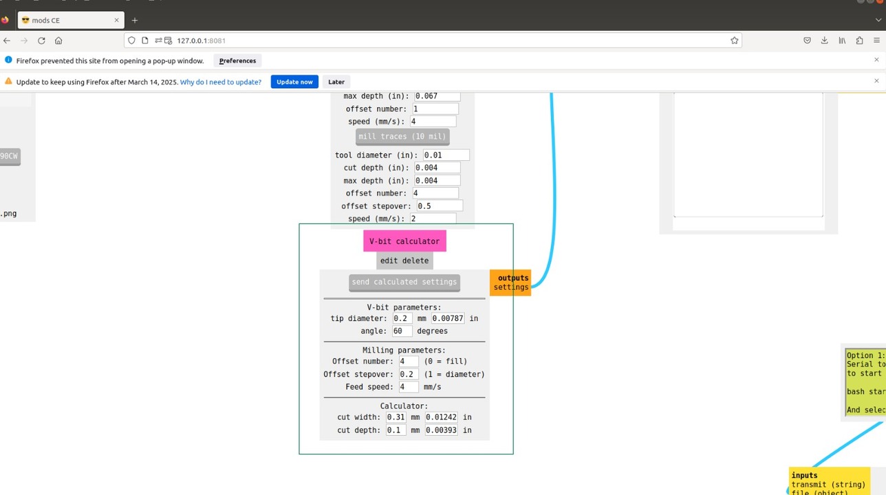
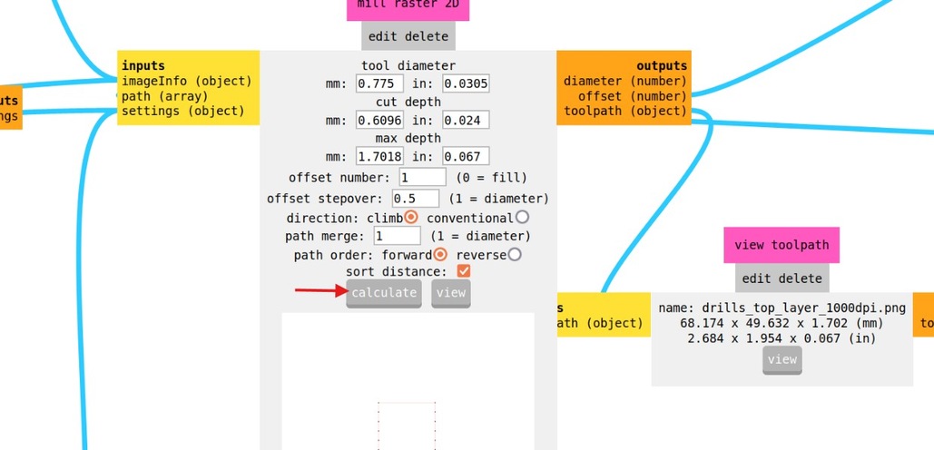
Load the png file to this node .
The next node ask you for the information regarding the tool diameter, depth and ...
For the traces click on vBit and enter dia ad 0.2mm and the degree as 60
Once that is set we can confirm the values on .mill raster 2D Node. After cross checking click on calculate.
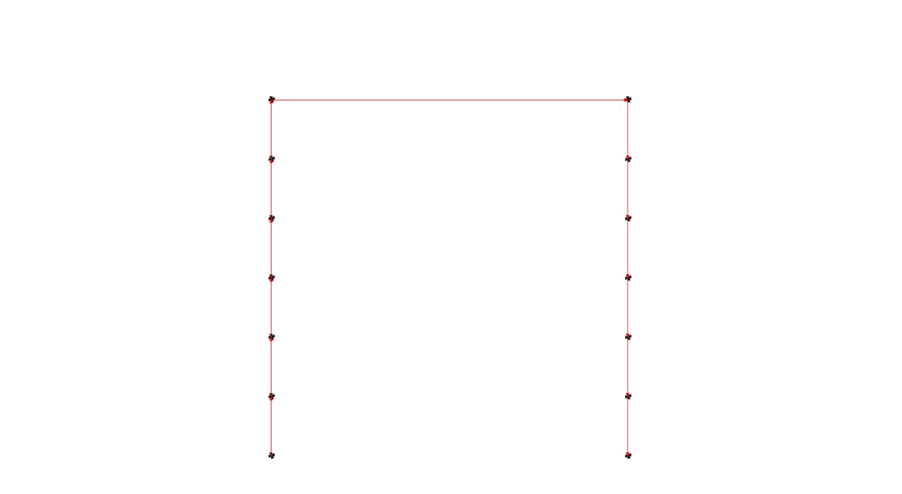
We can click on view to see how the traces will look with the offsets and the tool path.
Then we can click on send file for the machine to start milling.
Once the traces are done ,i moved on to drill holes as it was required in my design.
Clean up the dust gatherd after using the machine with a vaccum.
To make Holes and outlines
I needed to change the the toolbit to a 1/32" flat endmill to drill the through holes.
As we are changing the bit we need to follow the steps that we performed initially when we fixed the V bit.
In MODS replace the trace png with the dillholes png.
Since we changed the bit we have to modify the settings of the tool node
After confirming the values click on calculate. Then we can clcik send file to mmake the machine start the
operation.
After the holes are drilled, we can proceed to cut out the Outline of the PCB. We just need to replace the
drillhole png with
Outline Png for this step as we will be using the same toolbit for this operation.Click on send file to start the
process of milling the PCB.
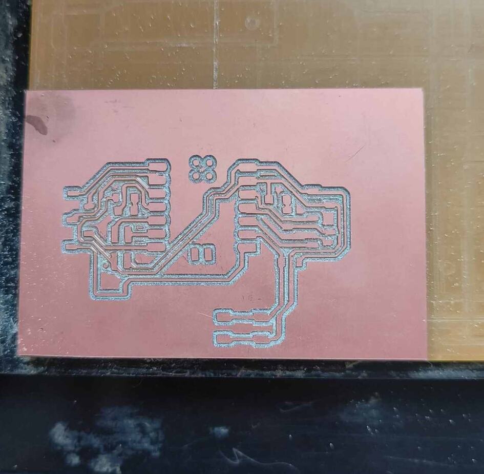
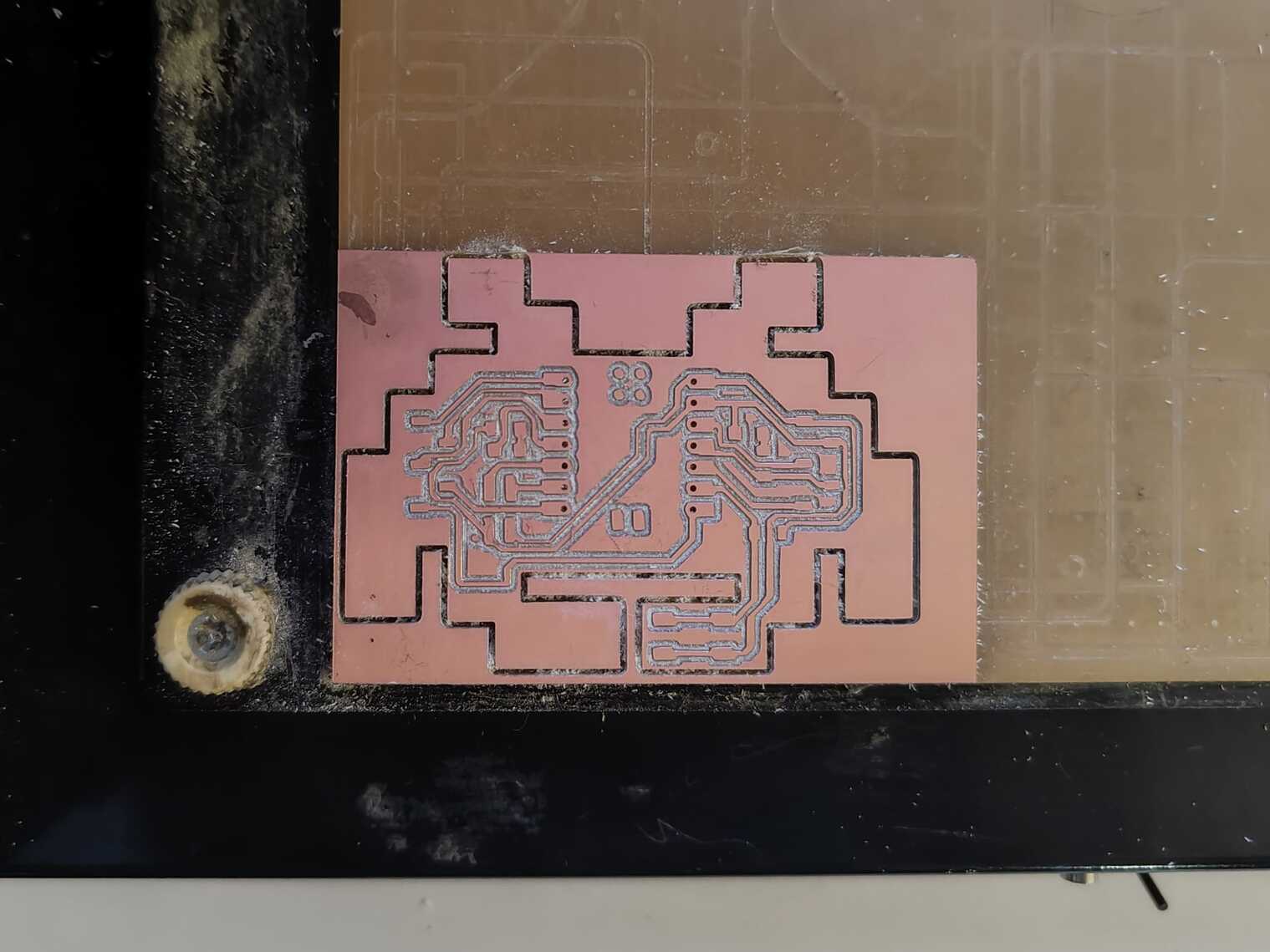
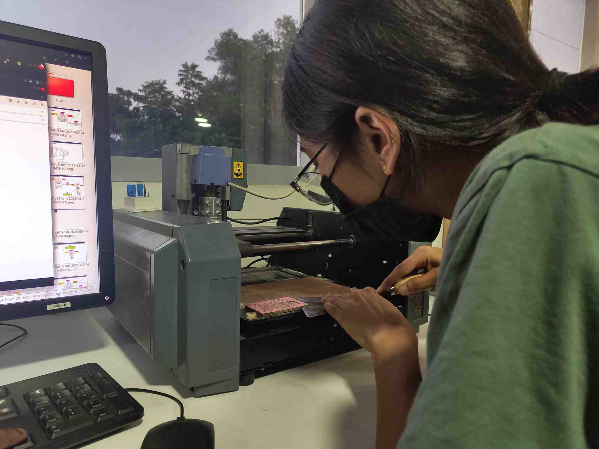
When the milling is completed we can click on view to bring out the bed. Use a scraper to carefully peel out the
pCB from the bed.
Make sure to clean up the dust gatherd around the machine after using it.
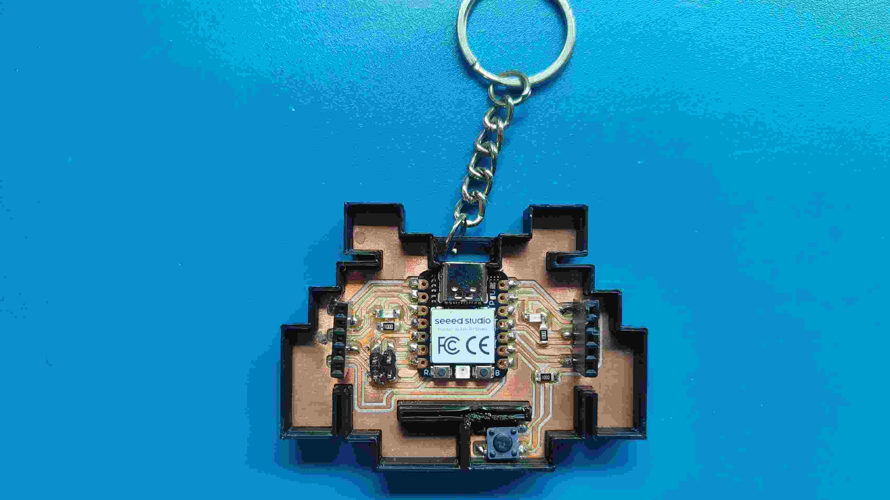
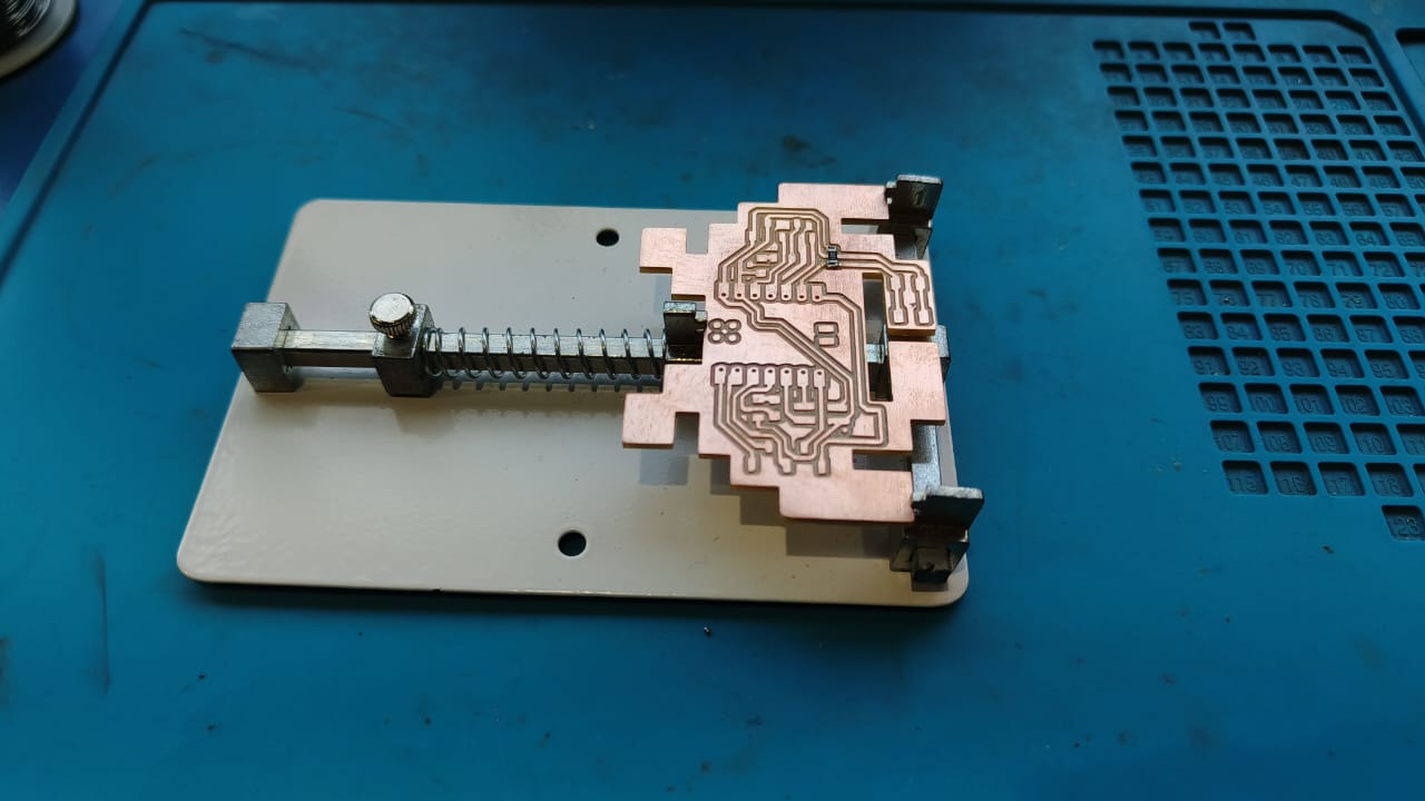
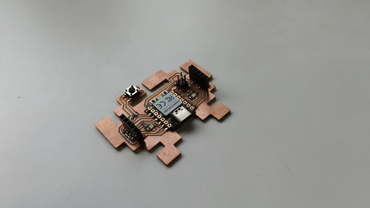
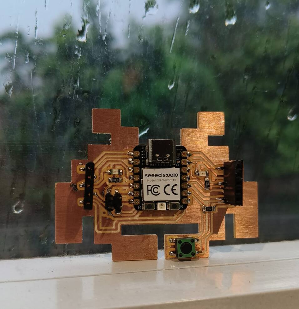
This was my PCB after cleaning the board.
The board with the components to be soldered
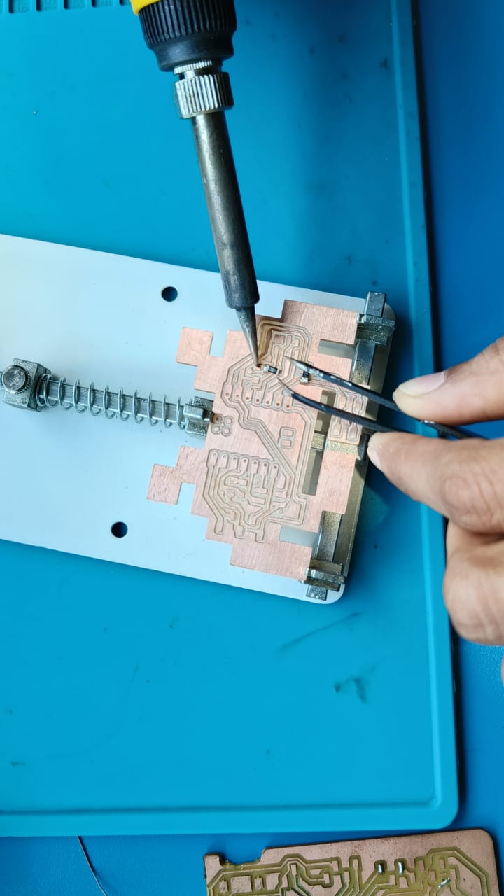
Soldering and Assembly of the components.
The soldering station was setup as guided and the PCB was clamped to keep it stable.
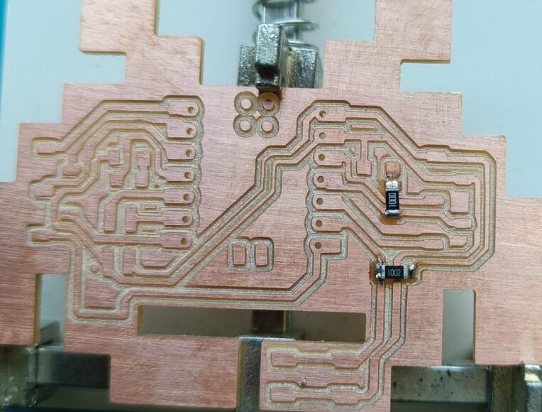
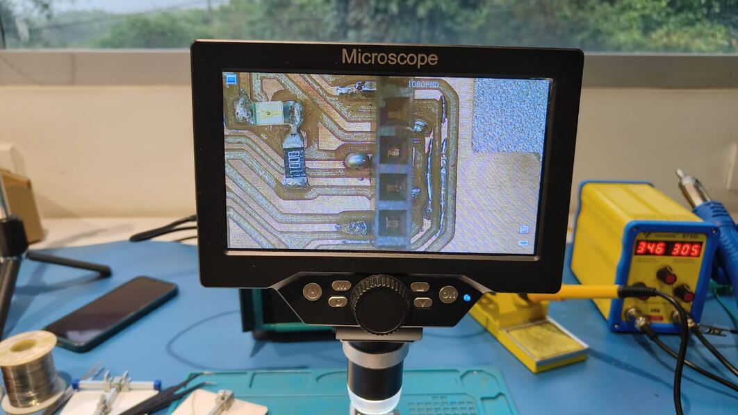
The parts were then soldered on to the pcb carefully
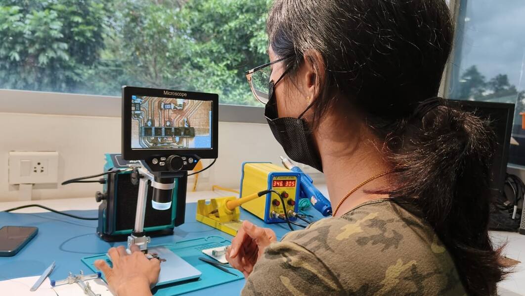
I inspected the solder closely. I found that i accidentally bridged a link but i corrected it.
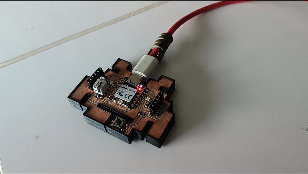
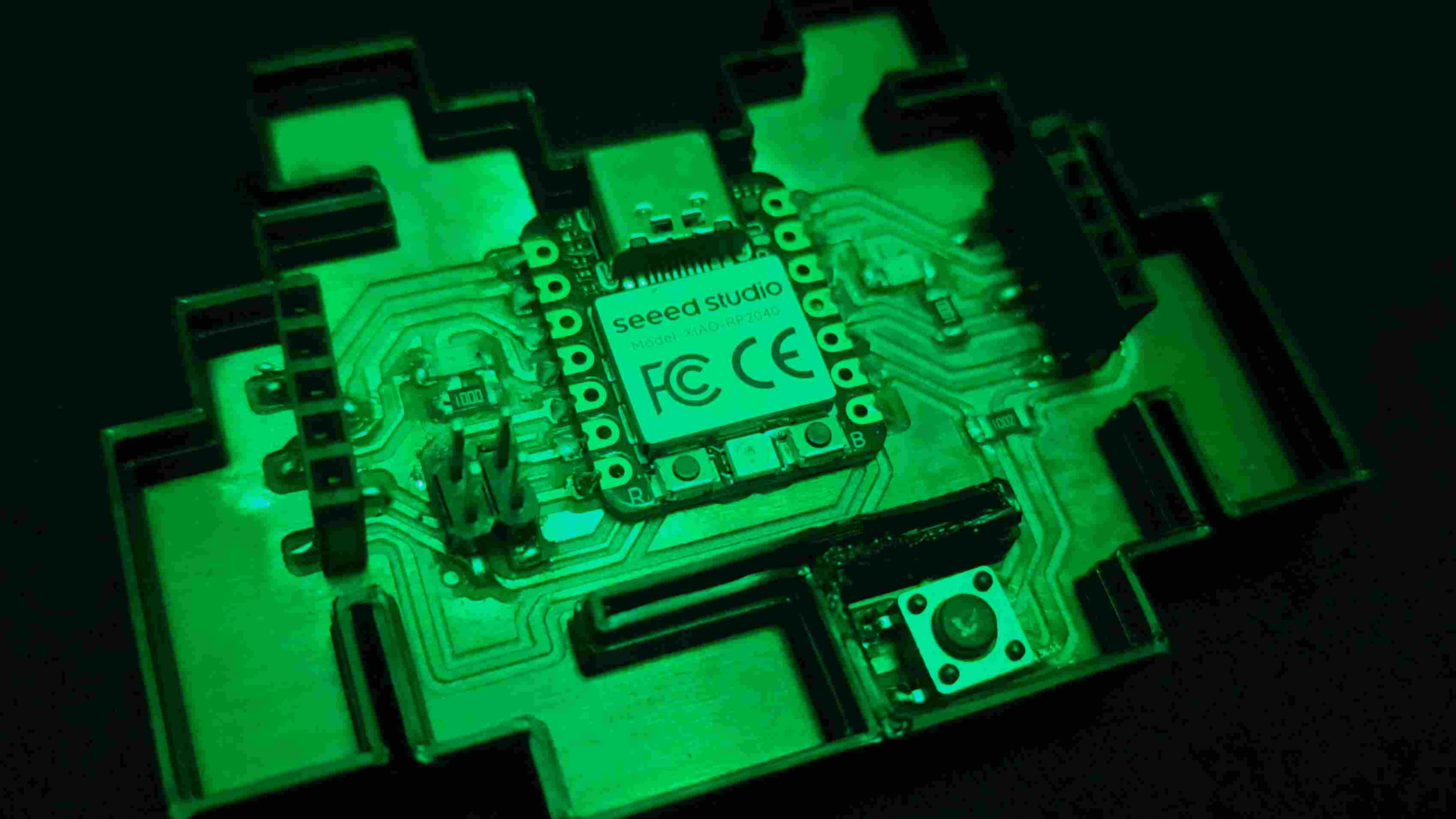
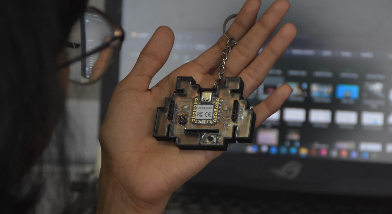
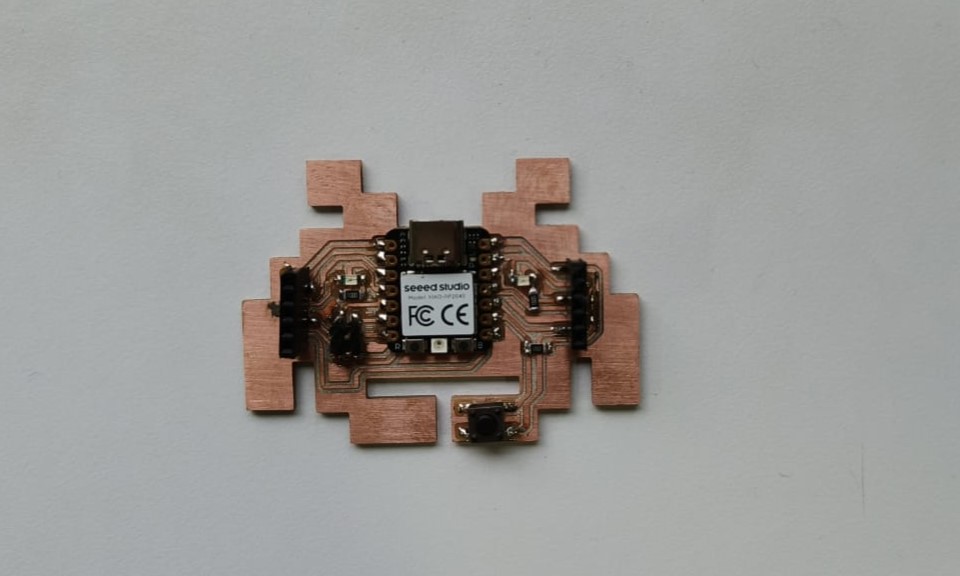
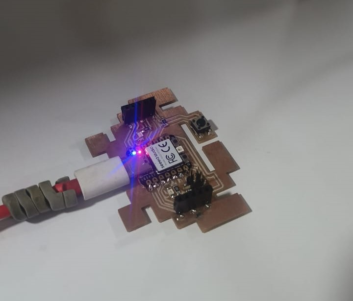
My assembled and soldered pcb looks like this:
Making my PCB blink
I followed the seed studio guide to setup the xiao rp2040
I wanted to make the leds blink continously as long as the switch is pressed. I ran a program to make the leds
work in Thonny using the following code. I played around to get the blink interval right for me.
#Code by Namita
#Code to make the Led on the PCB Blink

from machine import Pin
from utime import sleep

print("Hello, Pi Pico!")

led1 = Pin(3, Pin.OUT)
led2 = Pin(29,Pin.OUT)
button = Pin(2,Pin.IN)

while True:

        if button.value() == 1:
           print ("button on")
           led1.value (1)
           led2.value(1)
           sleep(0.1)
           led1.value (0)
           led2.value(0)
           sleep(0.1)


        else :
           led1.value(0)
           led2.value(0)
I changed the values of the switch to make the pcb stop blinking when the switch is pressed just for fun.
#Code by Namita
#Code to make the Led on the PCB Blink

from machine import Pin
from utime import sleep

print("Hello, Pi Pico!")

led1 = Pin(3, Pin.OUT)
led2 = Pin(29,Pin.OUT)
button = Pin(2,Pin.IN)

while True:

        if button.value() == 0:
           led1.value (1)
           led2.value(1)
           sleep(0.1)
           led1.value (0)
           led2.value(0)
           sleep(0.1)


        else :
           led1.value(0)
           led2.value(0)
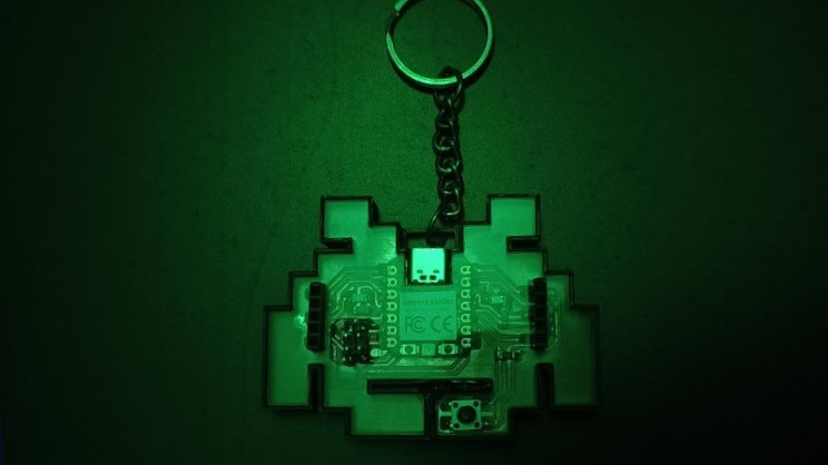
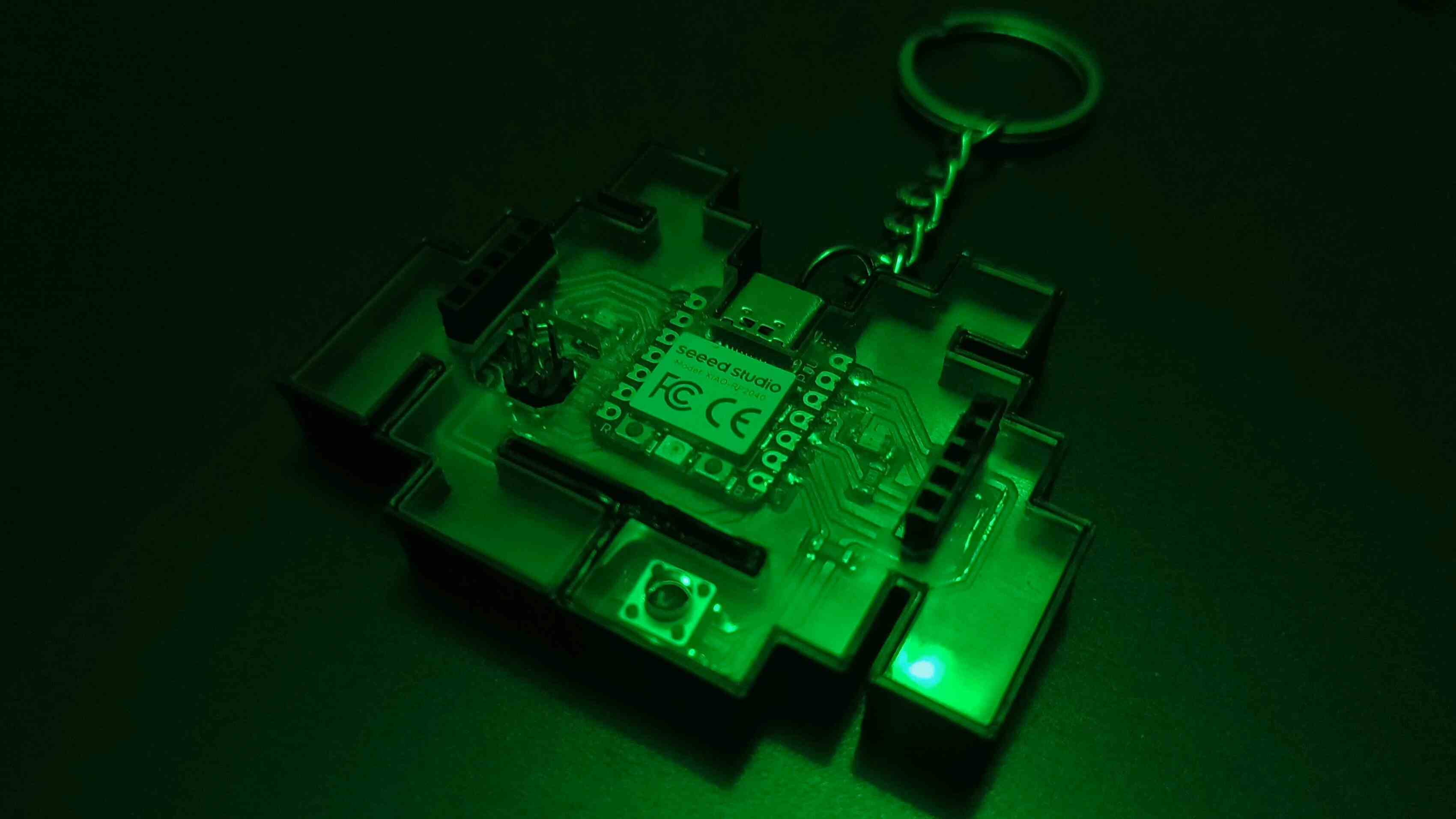
Making a case for the PCB
i had designed a case for the pcb in the last weeks' assignment. So went on to print the case.
Space Invader PCB
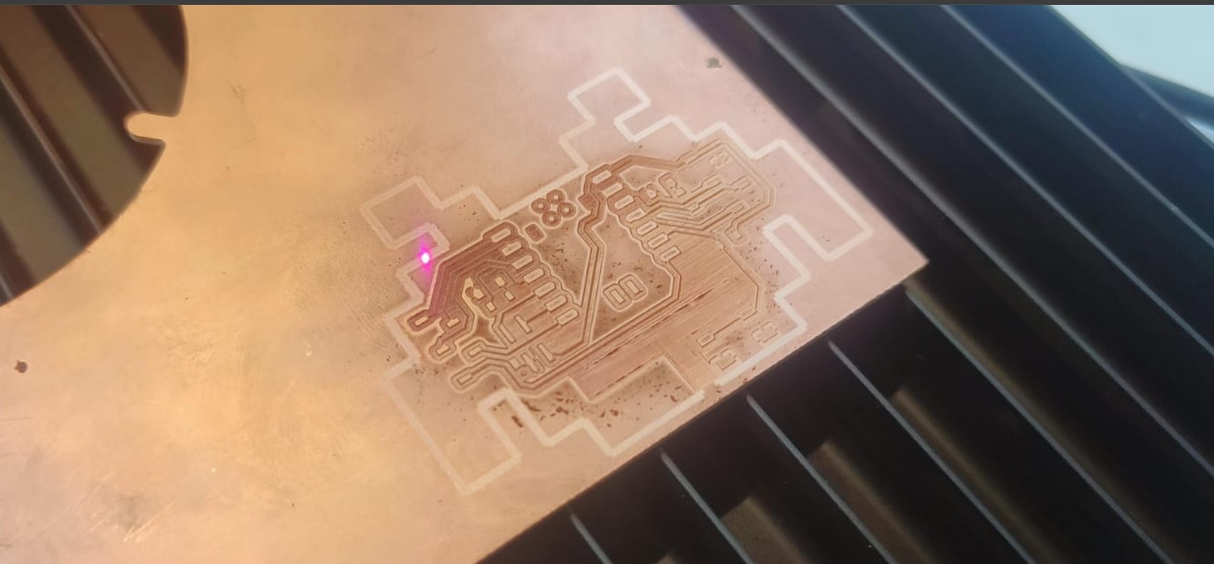
2. Making the PCB by laser engraving/cutting using Xtools F1 ultra
I wanted to make the the same pcd using laser engraving and the apply the solder mask to give its distinct
green colour that goes with the character too.
There was some issues while engraving. The machine was not taking off the copper layer. We are trying to
understand the issue to resolve it.


 There was some bug on the website that did not show the correct price of the components xD.
 We have to enter a series of commands related to the functioning of the machine.
We need the machine to do the traces in the beginning with a 0.2mm 60 degree V bit first , then we go on to do the
drilling
for the
holes and the outlines with a 1/32" flat endmill at the end.
We have to enter a series of commands related to the functioning of the machine.
We need the machine to do the traces in the beginning with a 0.2mm 60 degree V bit first , then we go on to do the
drilling
for the
holes and the outlines with a 1/32" flat endmill at the end.

.jpg)