6.Electronics Design
This week for :
Group assignment:
GROUP ASSIGNMENT
You can view our group assignment here!
INDIVIDUAL ASSIGNMENT
Printed circuit Board
PCBs are thin boards that contains electrical circuits that connect multiple components to form a complete system used to power our devices. The components are connected to the board by soldering them to the board. The board is made up of materials with poor conductivity the board can be of one , two or multi layers.
A PCB needs to be designed first before it cn be printed. This can be done on by PCB design CAD tools.
Components of a PCB
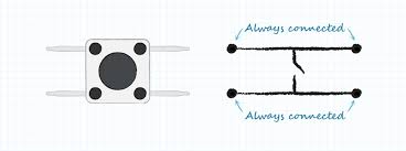
Switches:can either allow current or block depending if they are closed or open. There are several different types of switches available such as slider, push button, lever, toggle, key switches etc.
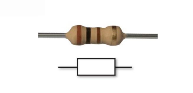
Resistors:Resistors are one of the most commonly used components in PCBs. They are used to resist the flow of current by dispersing the current flowing into it as heat.
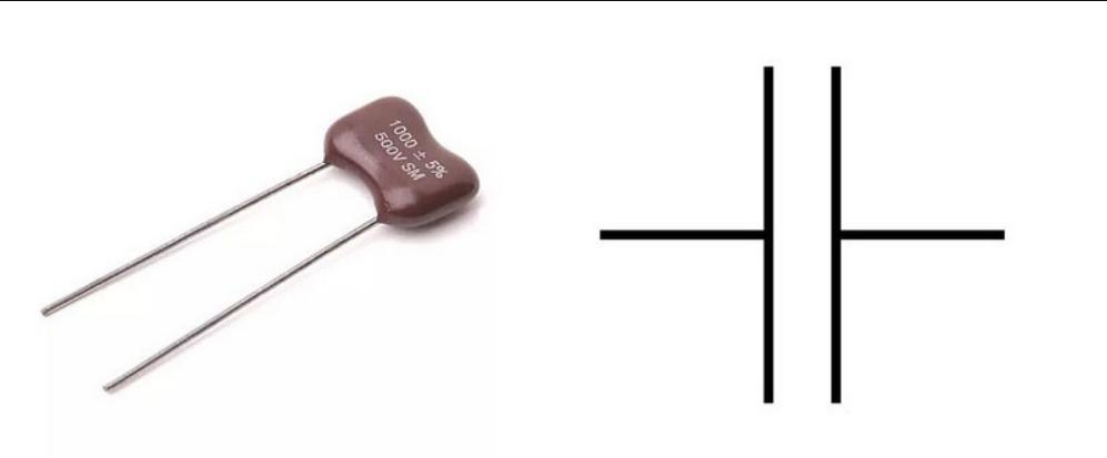
Capacitors: Another common component seen in PCBs. They temporarily hold electric charge and then dispersed whenever more power is required in th ecircuit. It functions by collecting opposite charges on two conductive layers with a insulating material in between.
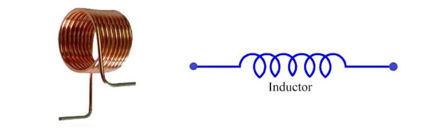
Inductors: They store energy in the form of magnetic field which is formed when current flows through an coil of wire. They are used to block or filter out certain signals.
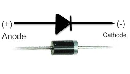
Diode: This device only allows current to flow from the anode to cathode i.e. only in one direction. This helps to stop current to flow not the wrong path which may cause damage. LEDs are semiconductor light sources that emit light when current flows through it in the correct direction.
Transistors: the are used to amplify the charge or as electronic switches. They can either be n-channel transistor or p-channel transistors. The NPN transistors .
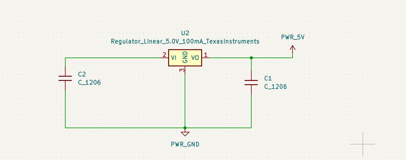
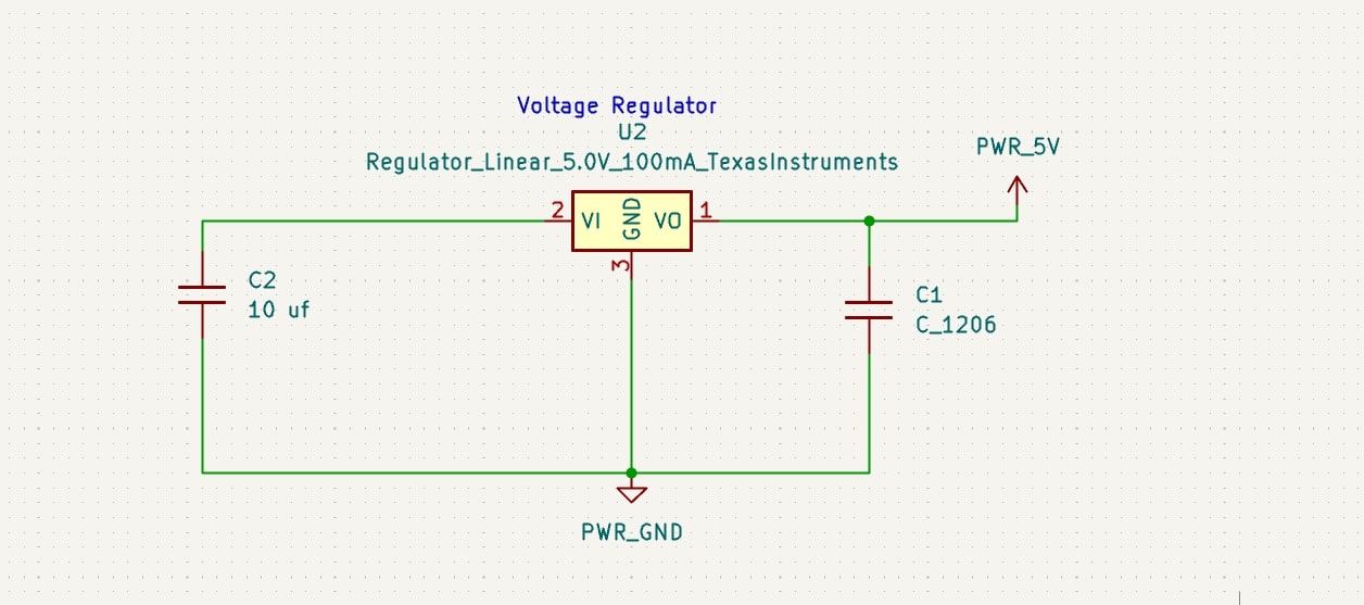
Designing a PCB
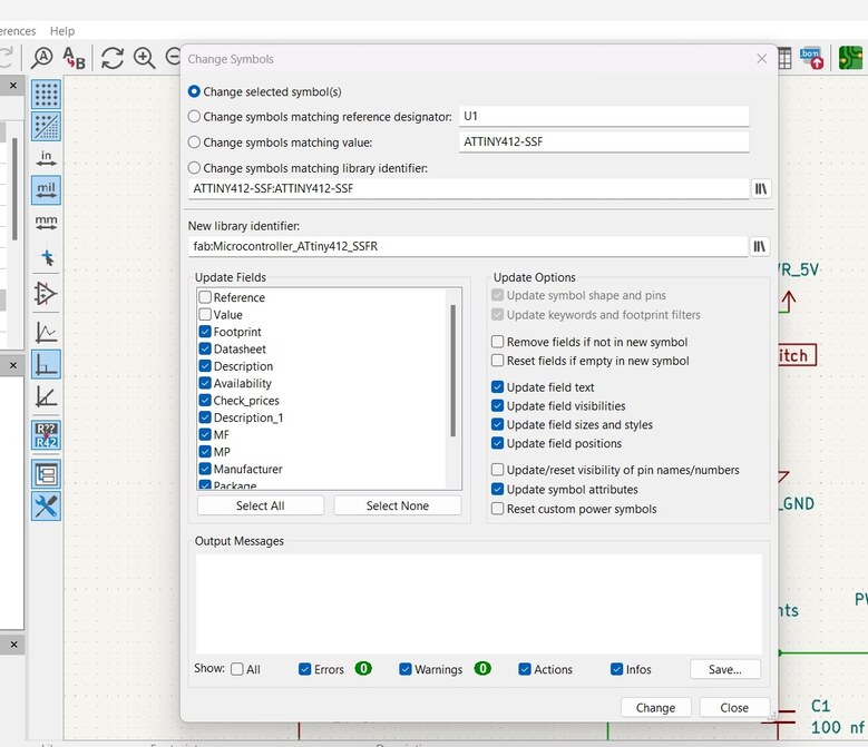
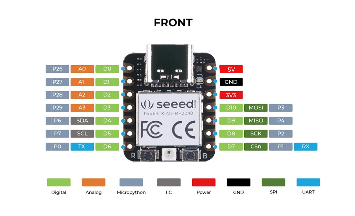
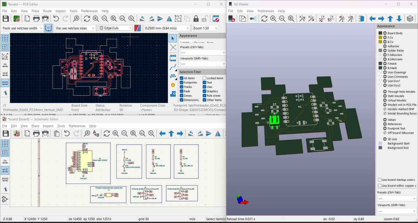
We have to design and map out a PCB before it is built. To do so we have to seek out CAD tools such as Eagle,EasyEDA,kiCAD,OrCAD etc. The software is used for designing the PCB is kiCAD.KiCad is an open-source Electronic Design Automation (EDA) software that helps users to create schematic diagrams of electronic circuits and convert them into PCB layouts and 3d models.There PCB design can be separated into 2 categories; schematic diagram of the the PCB and PCB layout to help design how the components will be mapped out physically on the board.
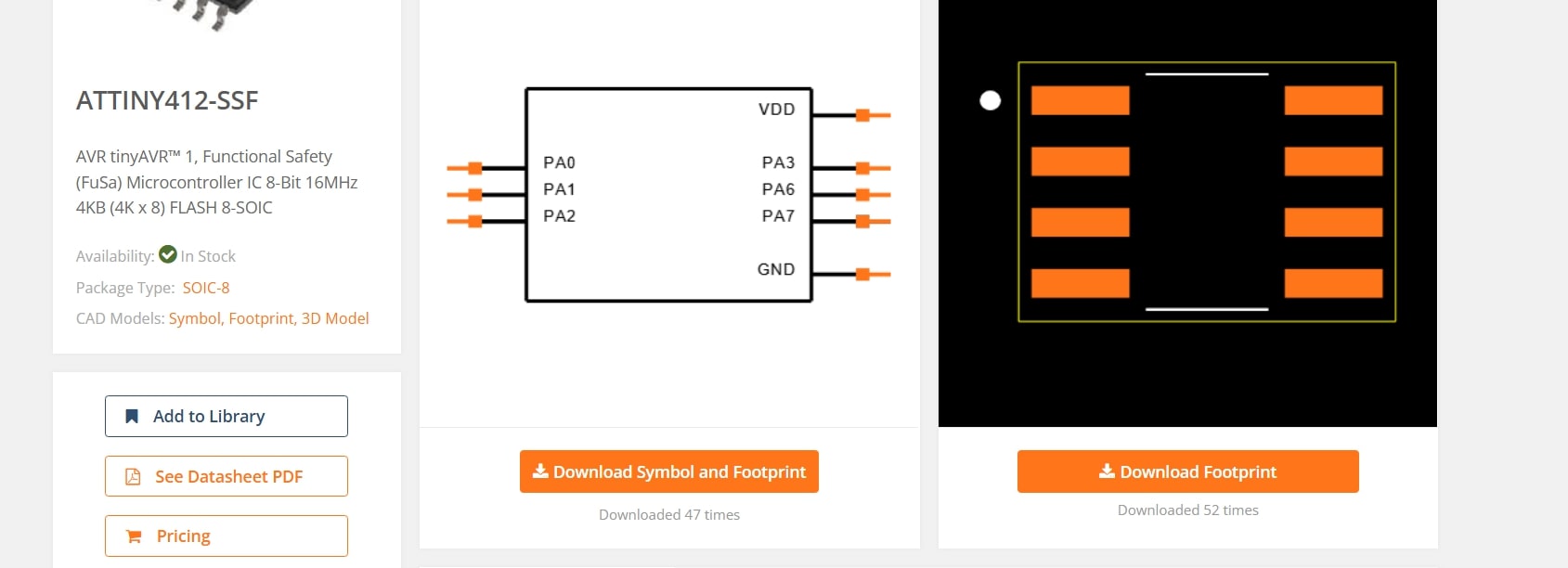
To access Fab Academy's library of symbols and footprints for KiCad, A .zip file is to be downloaded from https://gitlab.fabcloud.org/pub/libraries/electronics/kicad
Now we go to our GitLab profile and go to code and then copy the ssh key .
We now need to open GitBash in out Local kiCad folder and type in the clone command.
 Similarly to add footprints library:
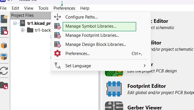
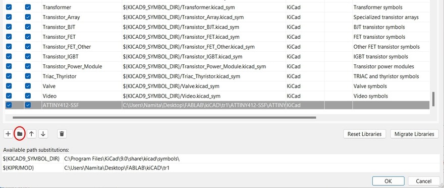
1.Open KiCAD. Go to preferences.
2.Click on 'Manage Symbol Libraries'.
3.Click on "Add file" and select the symbols library that we downloaded.
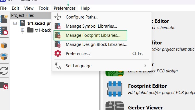
Similarly to add footprints library:
1.Open KiCAD. Go to preferences.
2.Click on 'Manage Symbol Libraries'.
3.Click on "Add file" and select the symbols library that we downloaded.
 This will import Fab Academy's symbols and footprints library into our KiCad project, so that we can access them
for the schematic design and PCB layout.
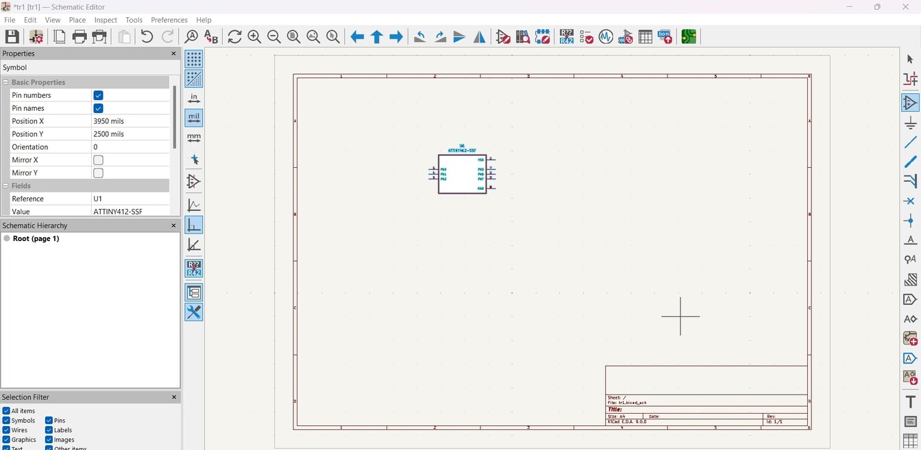
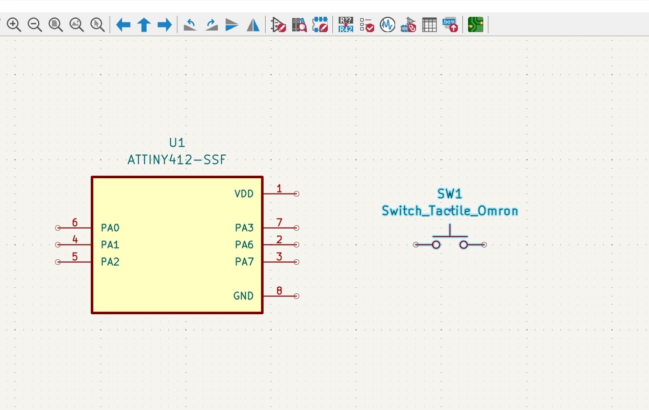
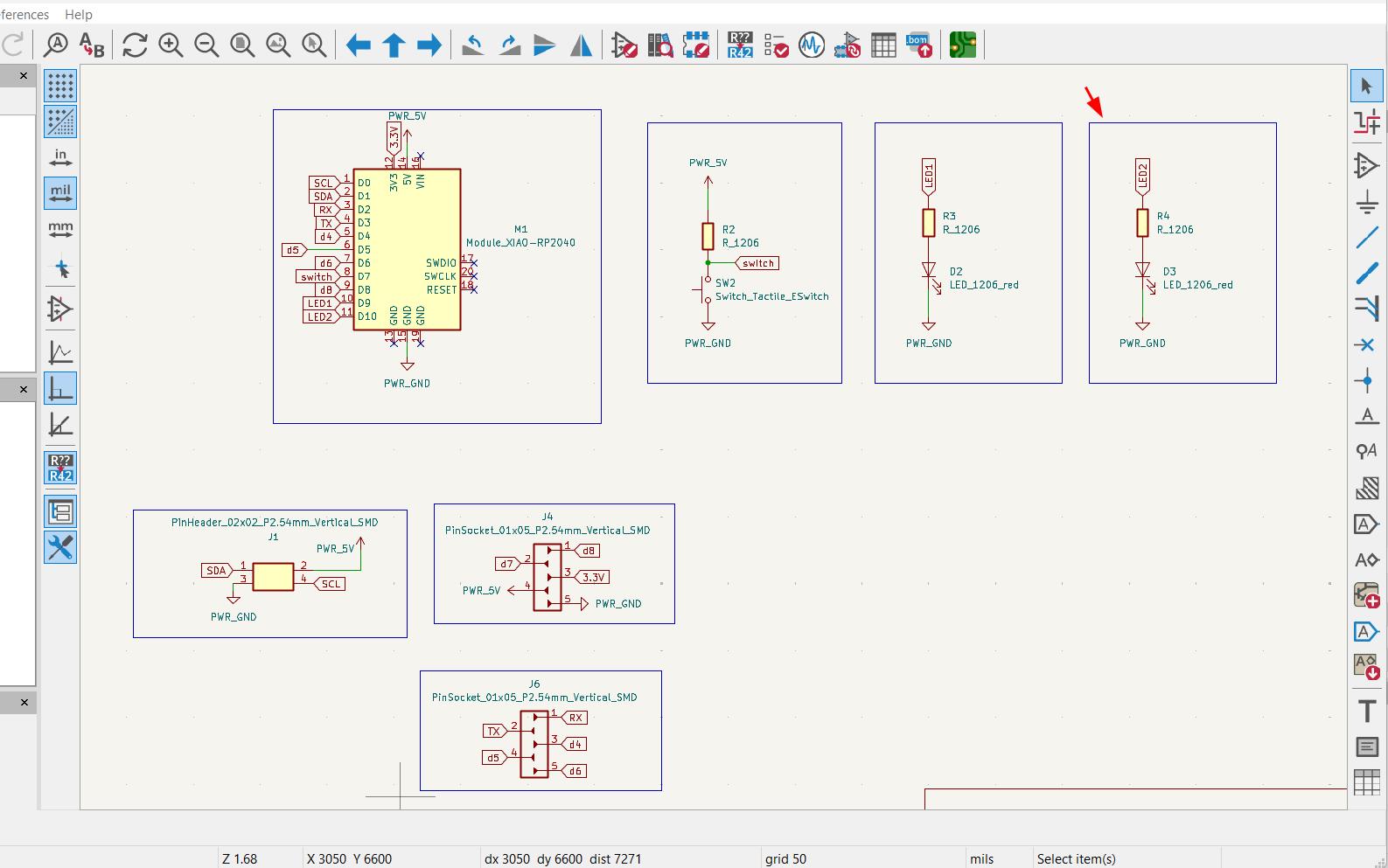
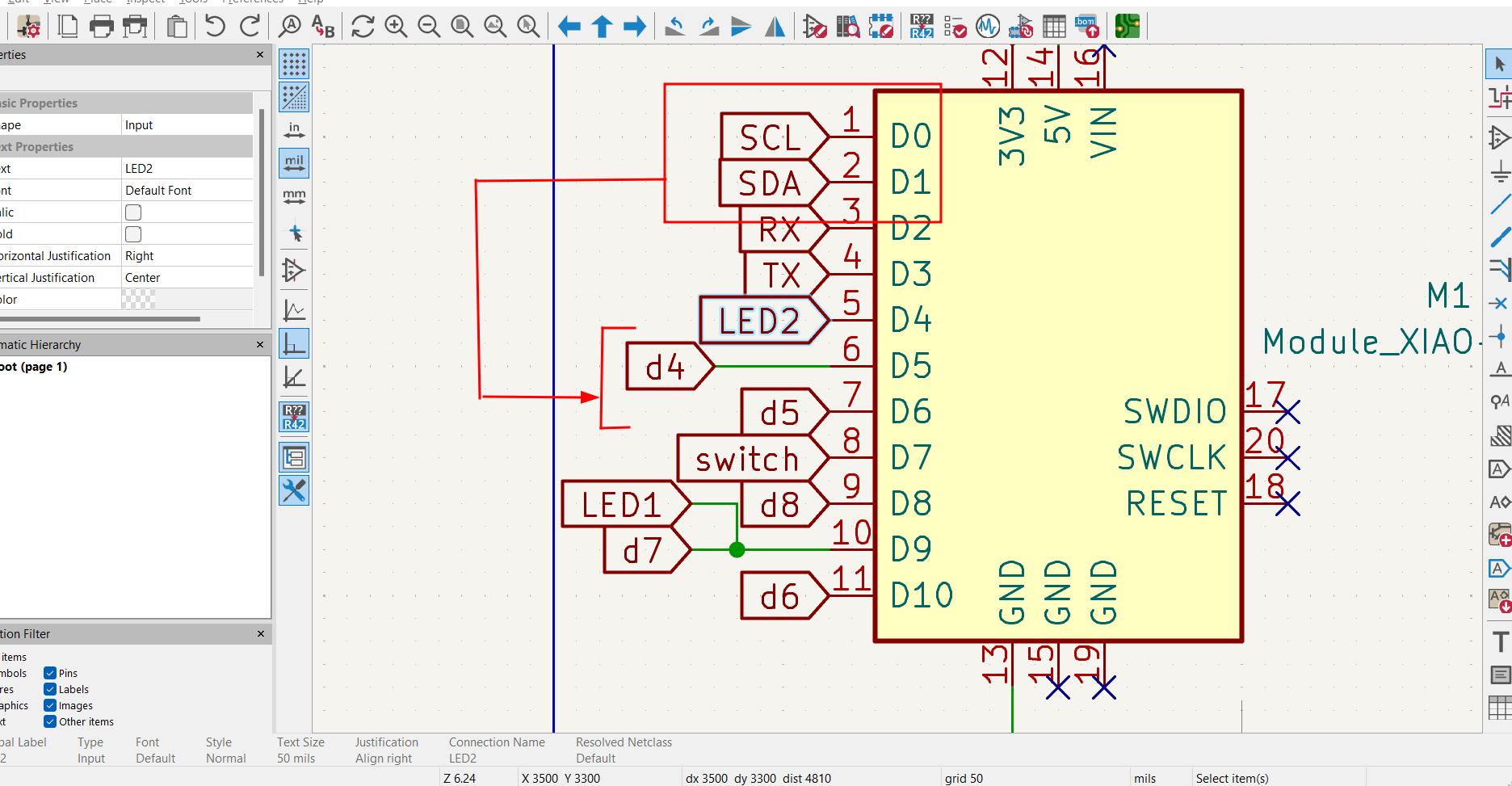
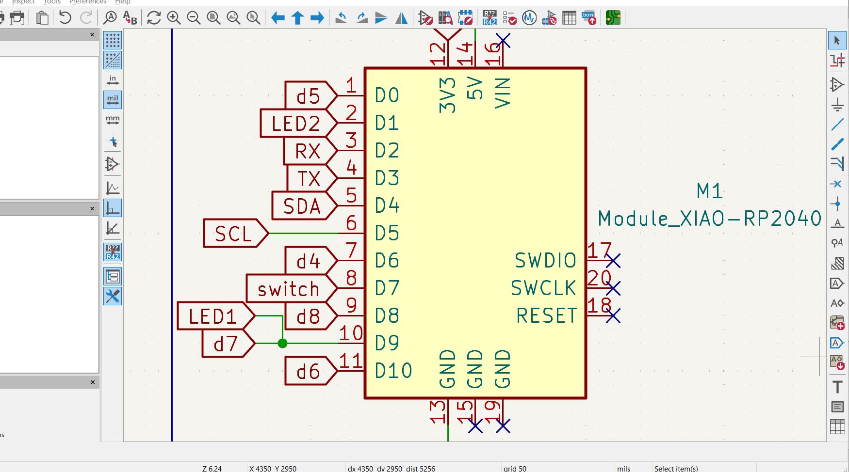
We start the bulid by working on the Schematic Diagram first. Since we were using kiCAD for the first time we did
a project just to understand the workflow of buildinga a PCB.
This will import Fab Academy's symbols and footprints library into our KiCad project, so that we can access them
for the schematic design and PCB layout.
We start the bulid by working on the Schematic Diagram first. Since we were using kiCAD for the first time we did
a project just to understand the workflow of buildinga a PCB.
To insert the symbols file into KiCad, follow these steps:
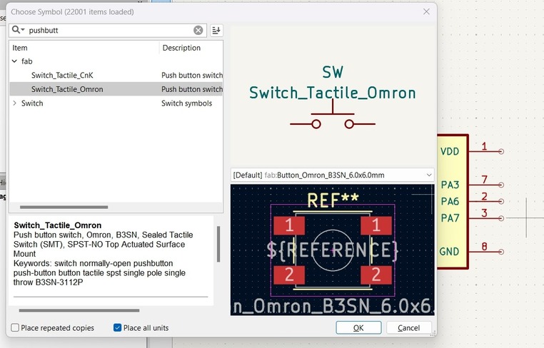
adding a switch
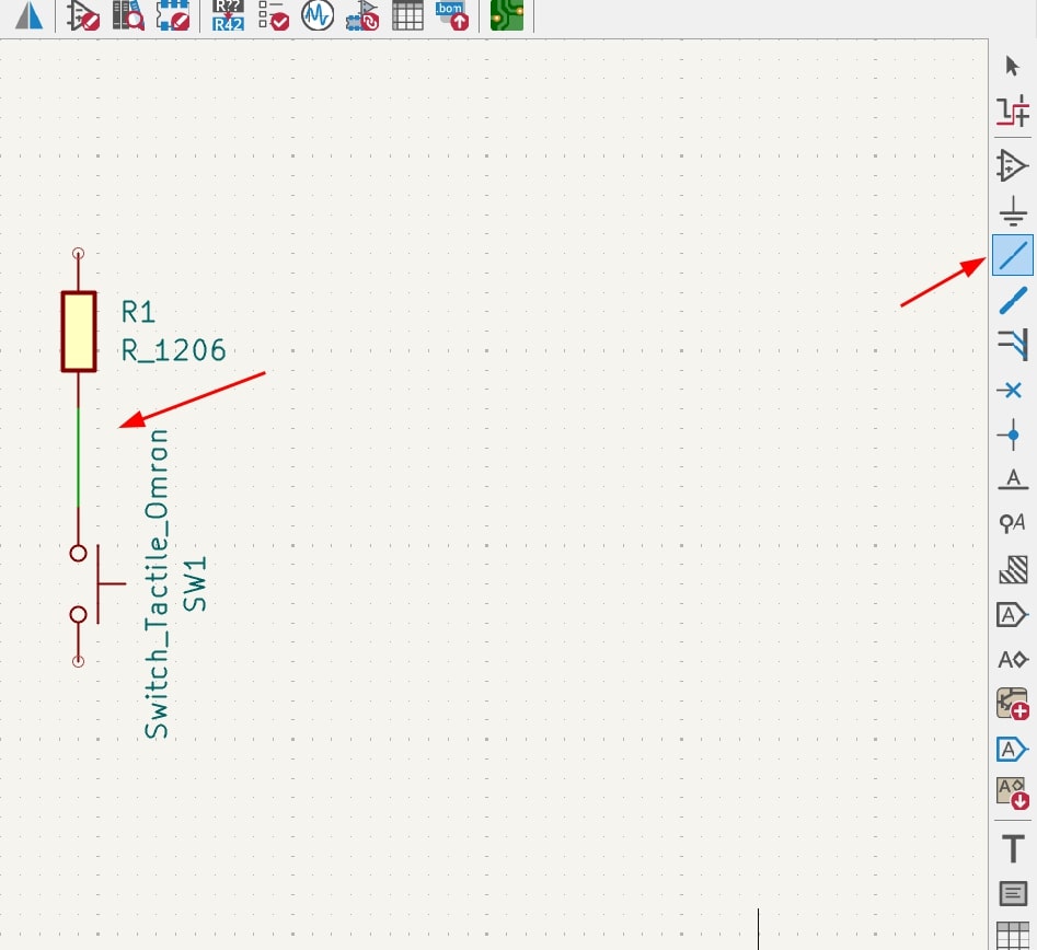 Use the draw line command ( shortcut key 'L') to draw wire connecting
the parts.
Use the draw line command ( shortcut key 'L') to draw wire connecting
the parts.
We can name each section of the circuit using the text tool from the tool bar.
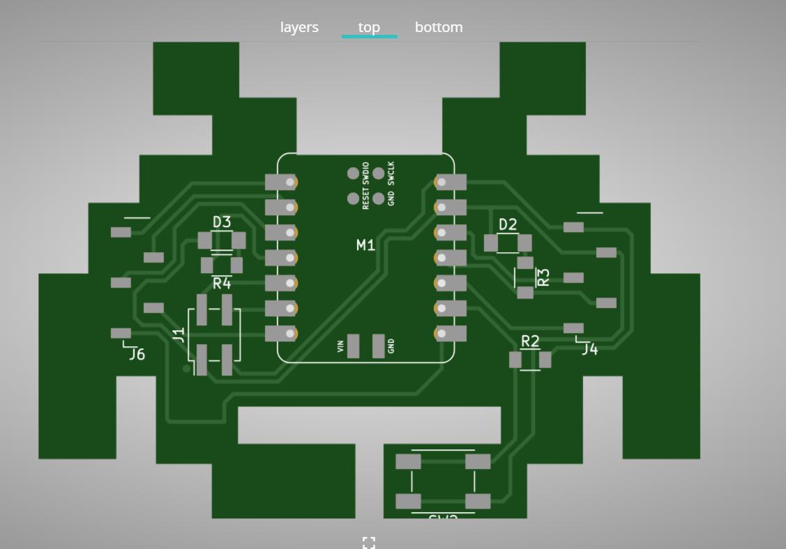
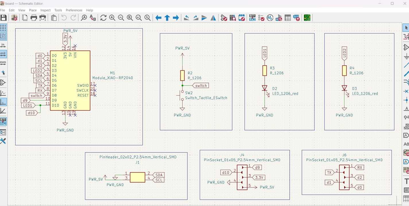
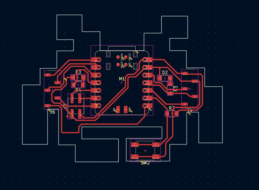
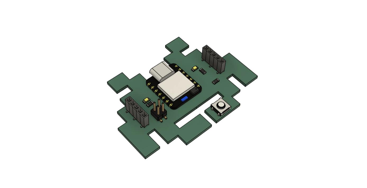
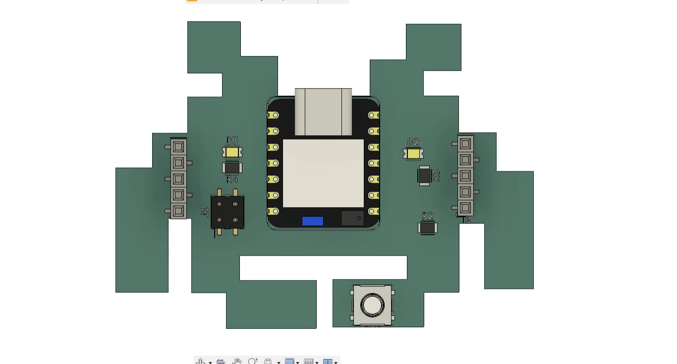
Designing a custom PCB
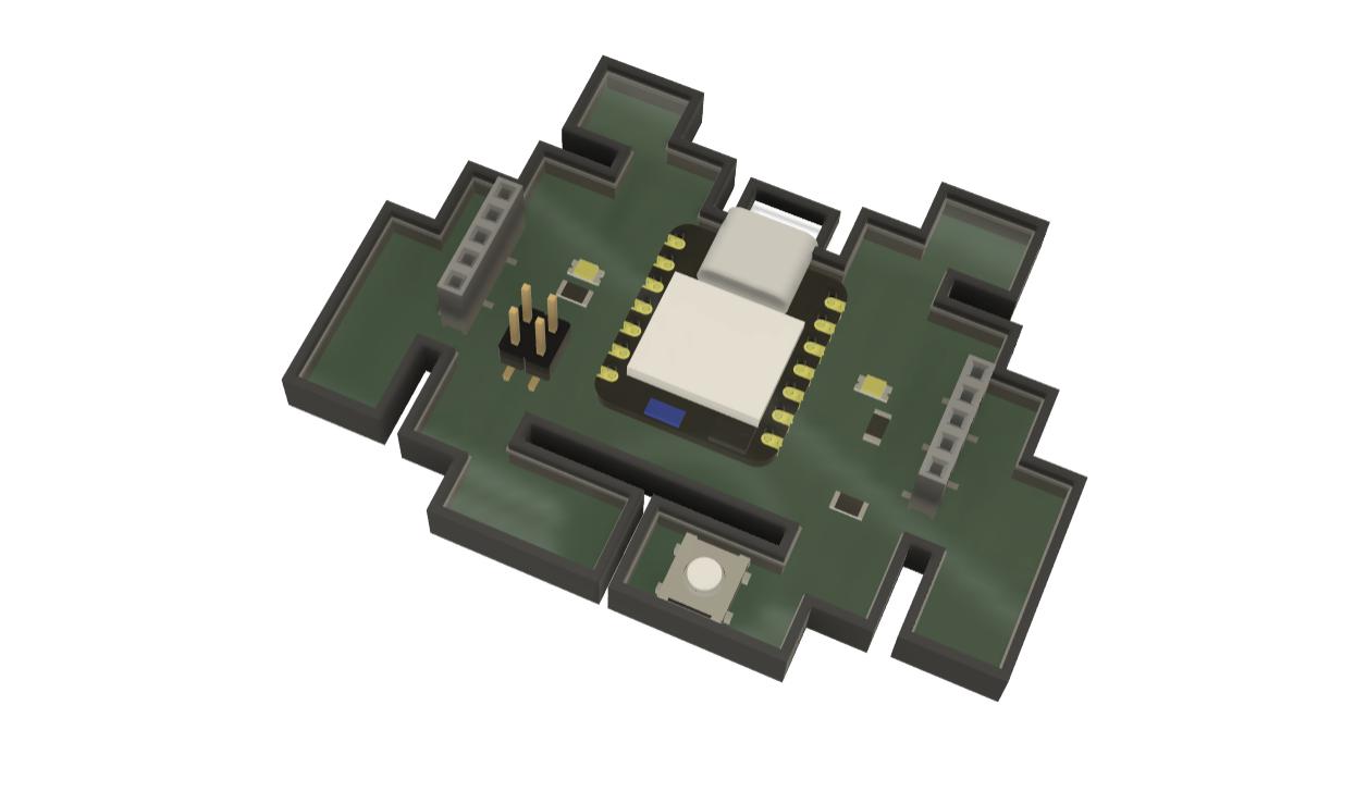
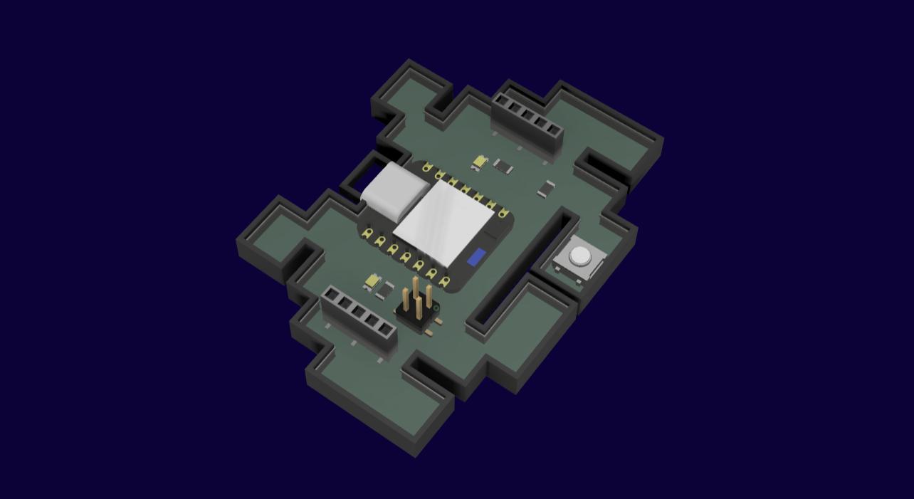
For this assignment we could create a custom PCB by ourselves. I wanted to use a 'Space Alien Invader'
video game
character as the shape of my board, because for some reason they remind me of PCB boards!


The components i used are
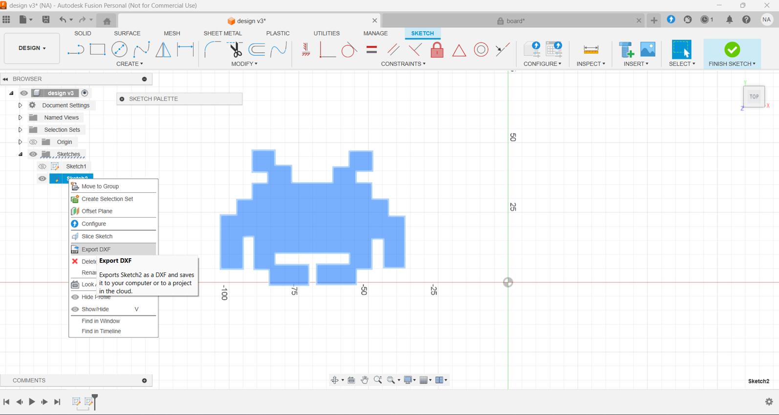
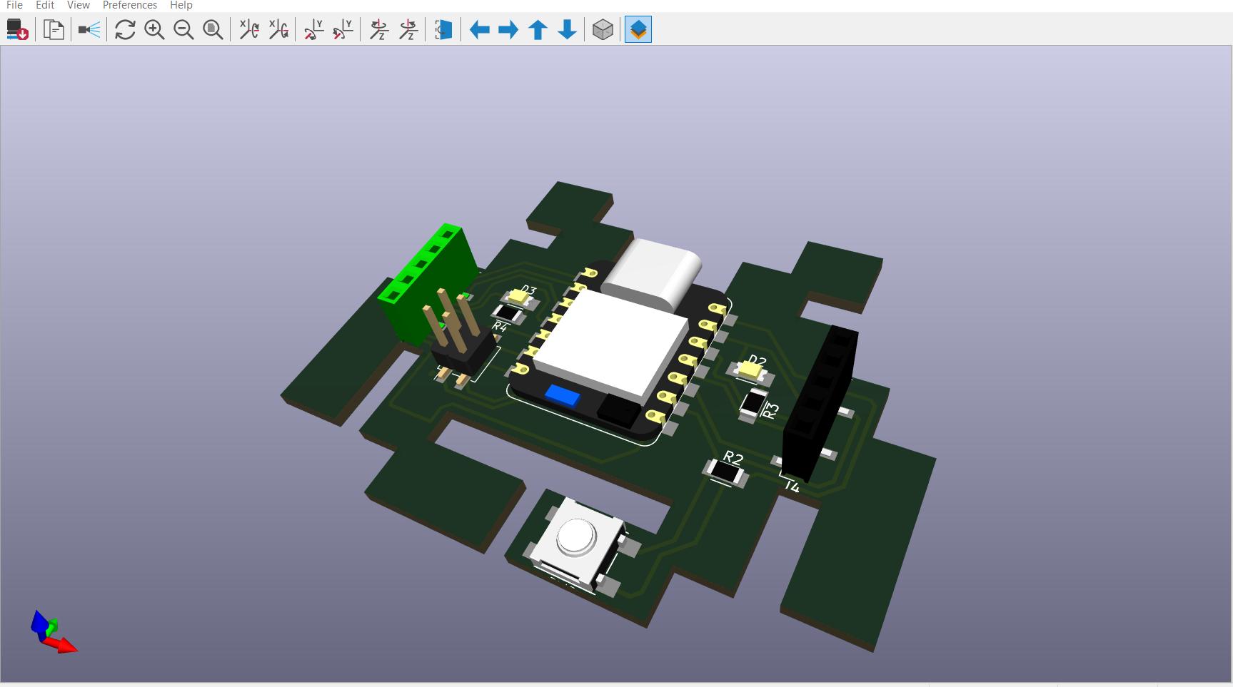
Creating a case for the PCB
I modeled a case for the PCB on fusion360. I also added a keyring hole so that it can be attached to a chain or hook.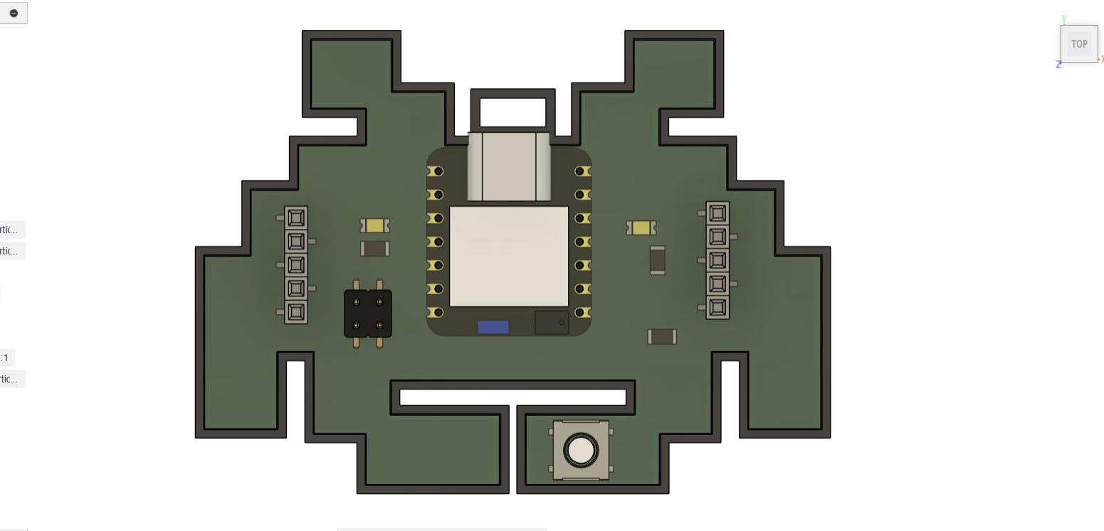
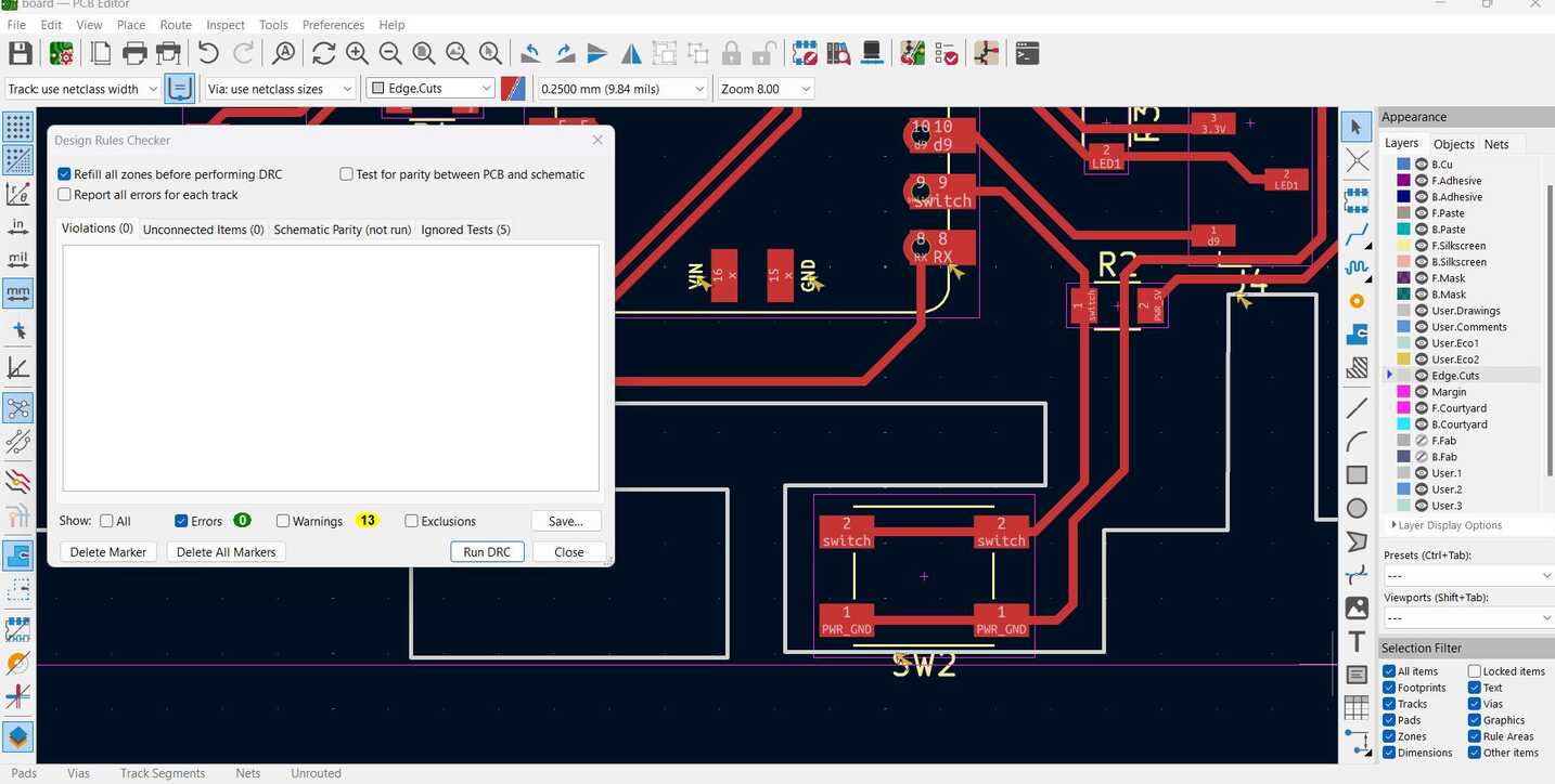
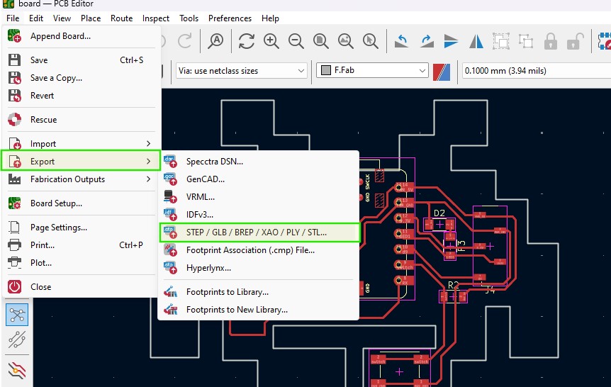
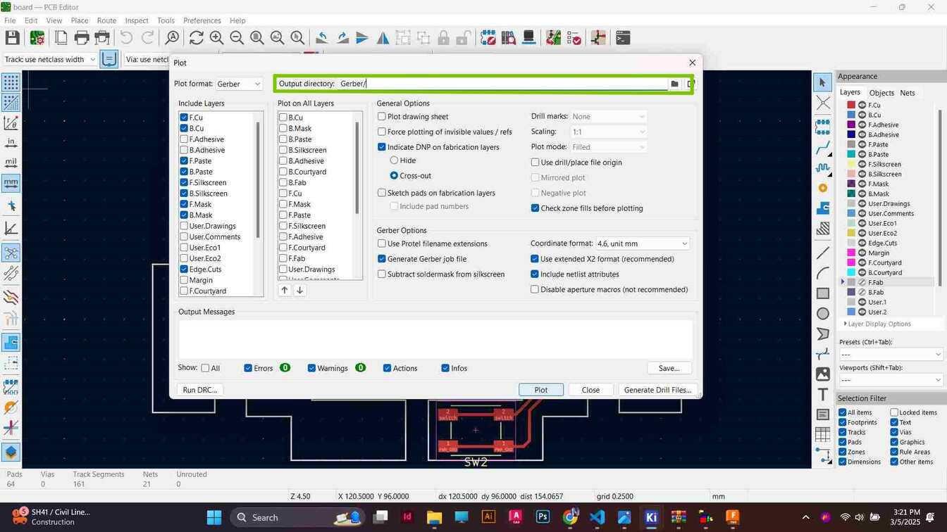
Making a Gerber File
The file we have currently needs to be converted into a gerber file so that it can be sent for manufacturers of the PCB. Gerber is a standard file format that contains the design data for a PCB. It includes the differnt layers PCB's , including copper traces, solder mask, and silkscreen, position of each component, such as pads, vias, and drill holes etc. To create a gerber file Go to Fabrication outputs> Gerber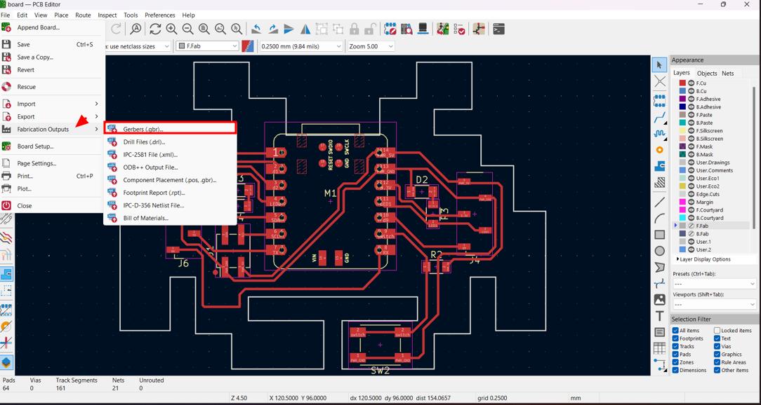 A plot dialogue box appears. On the output directory field enter "/gerber". This is done so that a gerber folder with all the files will be plotted in one place.
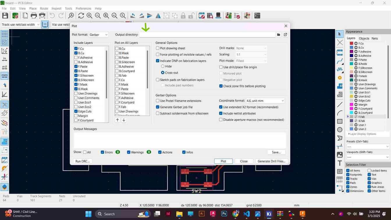
 Click on Generate Drill files
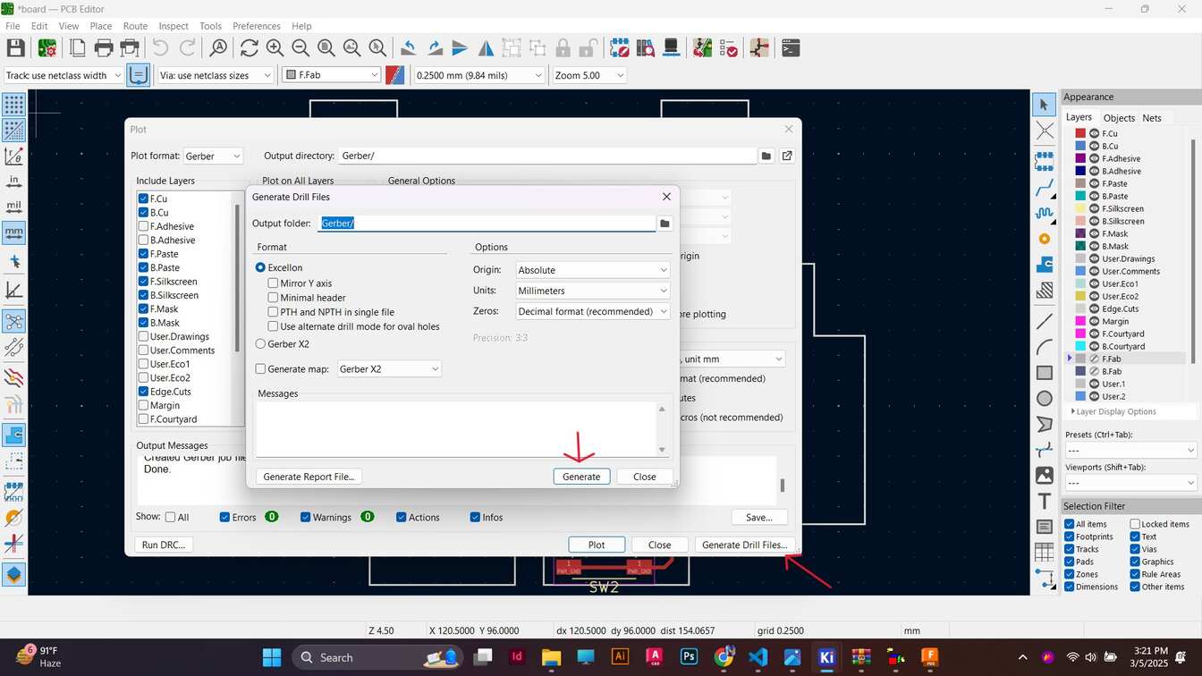 Then click plot. Now go to PCBway and drop the files within the gerber folder we created there. The PCB will be generated using the information.