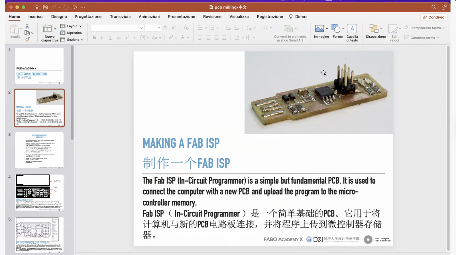
Week 06 — Electronics Design
Documentation
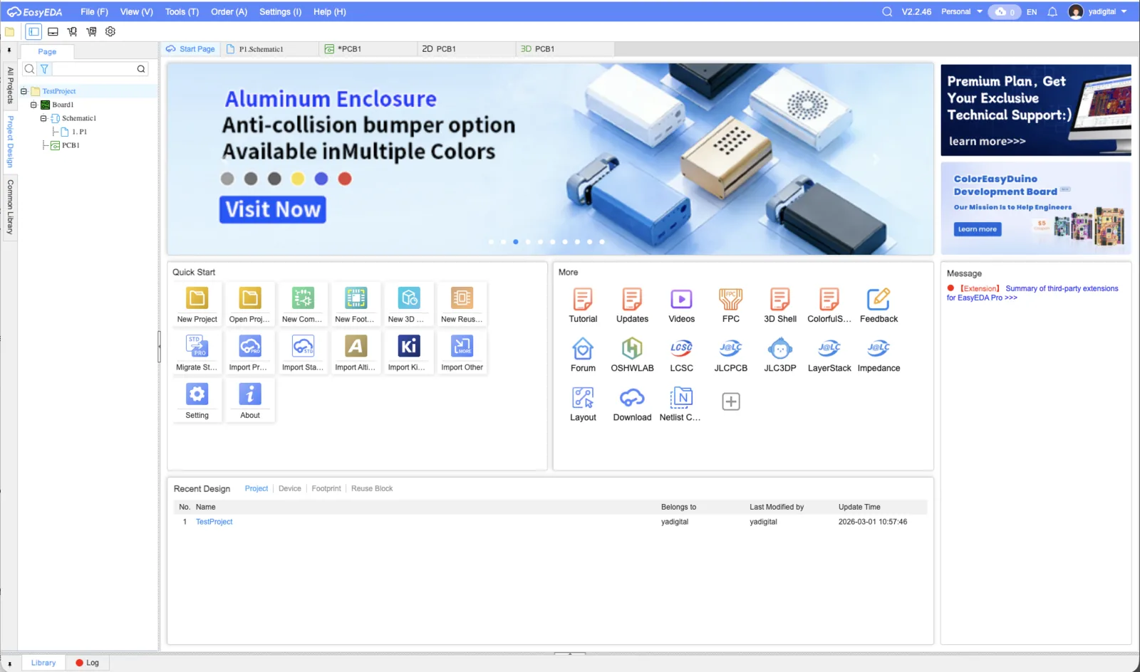
This week I focused on learning a complete electronics design workflow for a small embedded board. I first tried several EDA tools, then chose EasyEDA for this assignment, built a schematic around the XIAO ESP32-C3 form factor, added a button and LED as input/output components, checked the fabrication rules, and exported the final board for production.
Group Assignment
- Use the test equipment in your lab to observe the operation of an embedded microcontroller.
Individual Assignment
- Simulate a circuit.
- Use an EDA tool to design an embedded microcontroller system using parts from the inventory, and check its design rules for fabrication.
- Extra credit: try another design workflow.
- Extra credit: design a case.
Trying Different EDA Tools
I started by installing KiCad and the Fab library plug-ins. The installation itself was straightforward, but the environment felt unfamiliar and I could not move quickly yet.
I also installed Autodesk Eagle, but the result was similar. I understood that I would need much more time to be comfortable in that interface.
After a workshop with classmates, I switched to EasyEDA. For a first electronics design assignment, the online workflow felt much easier to understand. I also looked at LCEDA and existing Fab Academy examples to understand what kind of board I wanted to make.
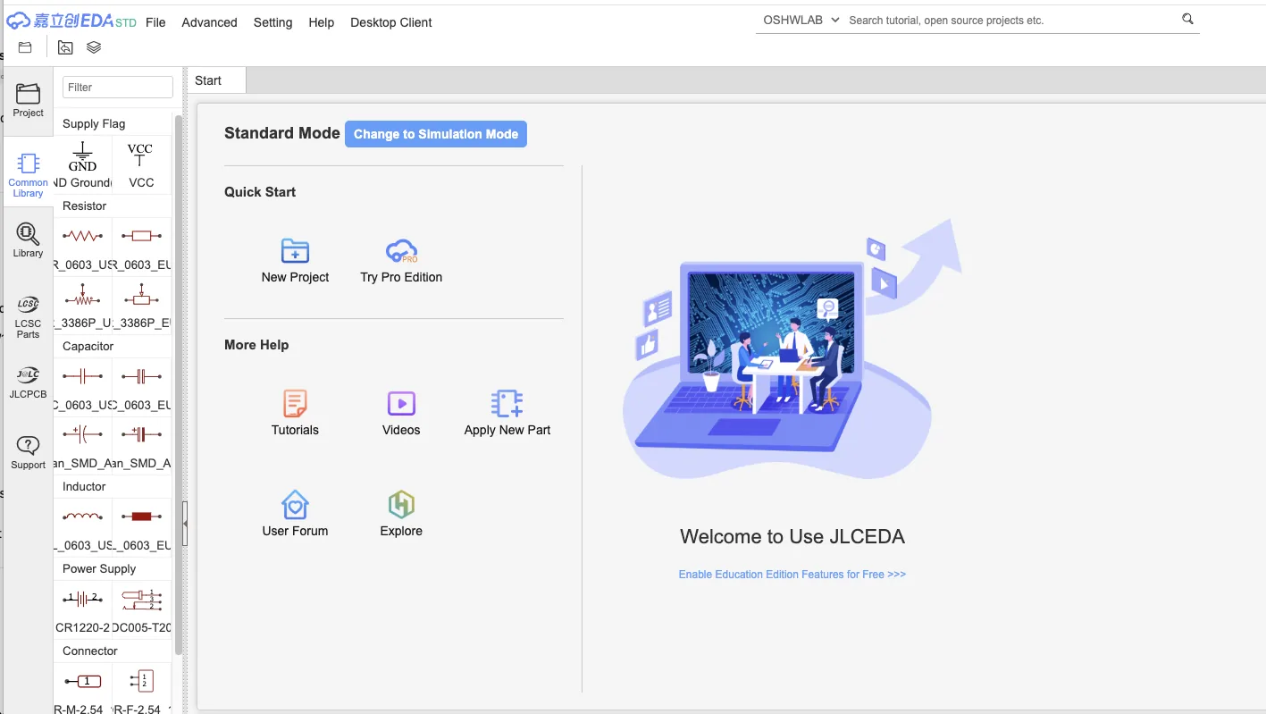
EasyEDA
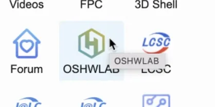
On EasyEDA interface, we can also observe different projects using this icon OSHWLAB. This is a project from other users, and it's worth scrolling and exploring something interesting.
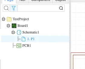
When creating a new project, we can see two files: schematic and PCB. These two files are created together and they will reflect changes from each other. Usually, first we need to edit the schematic, and then we can adjust the PCB. For adding new electronic components in a schematic, we can press this electronic chip icon, and then we can find the library of components and select what we need.
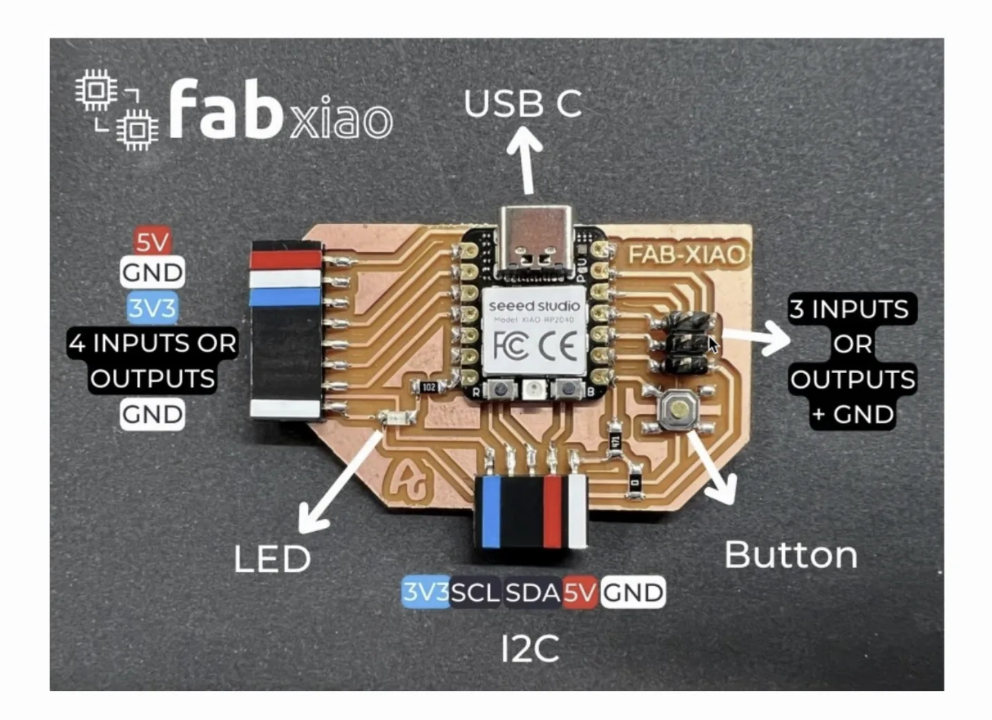
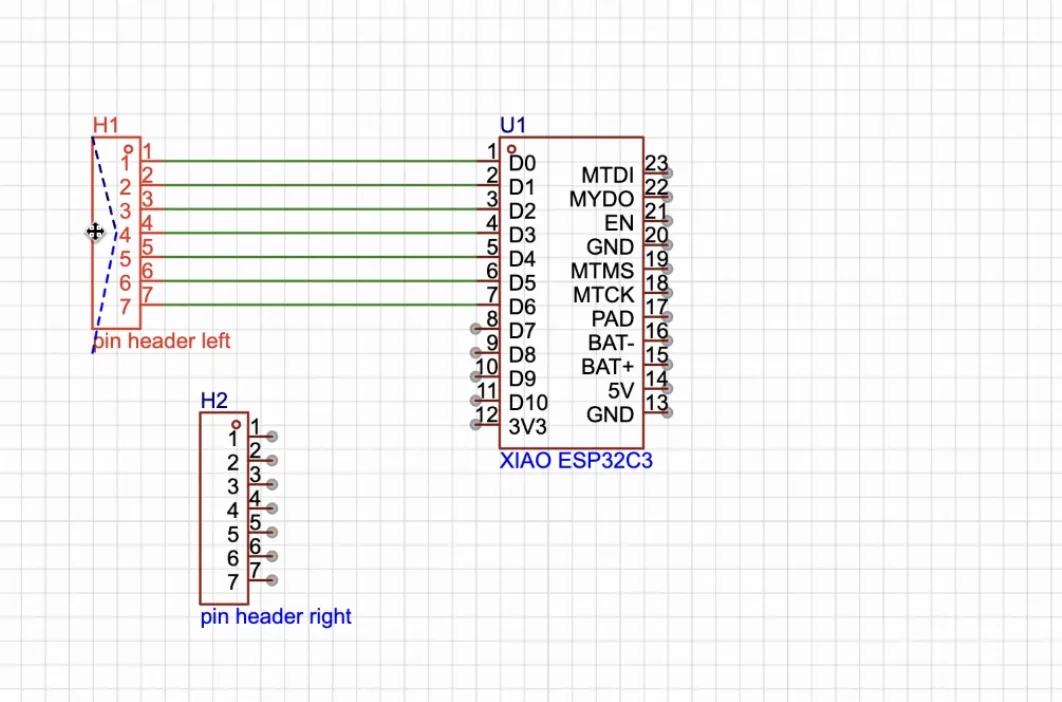
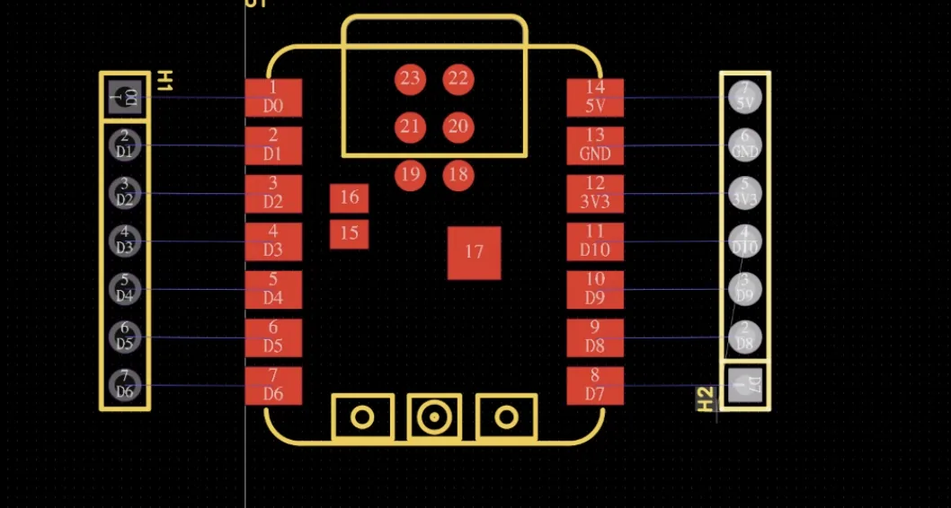
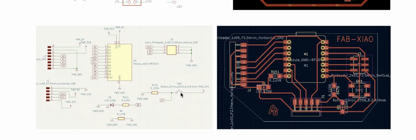
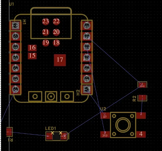
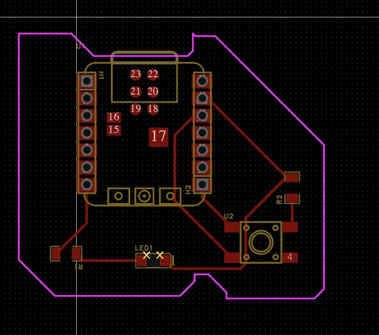
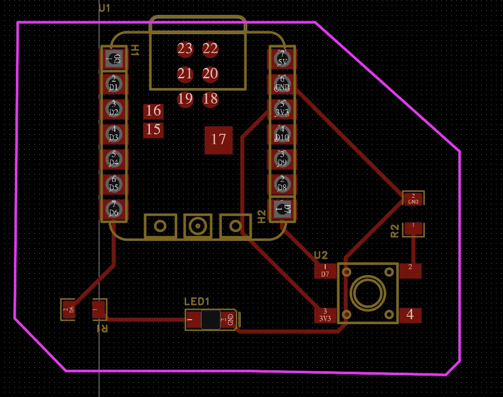
Board Concept: A Universal XIAO Carrier
My idea was to design a PCB that can hold different XIAO boards with the same form factor. The exact chip can be different, but the footprint is similar, so a small carrier board with headers, an LED, and a button can be reused for several boards.
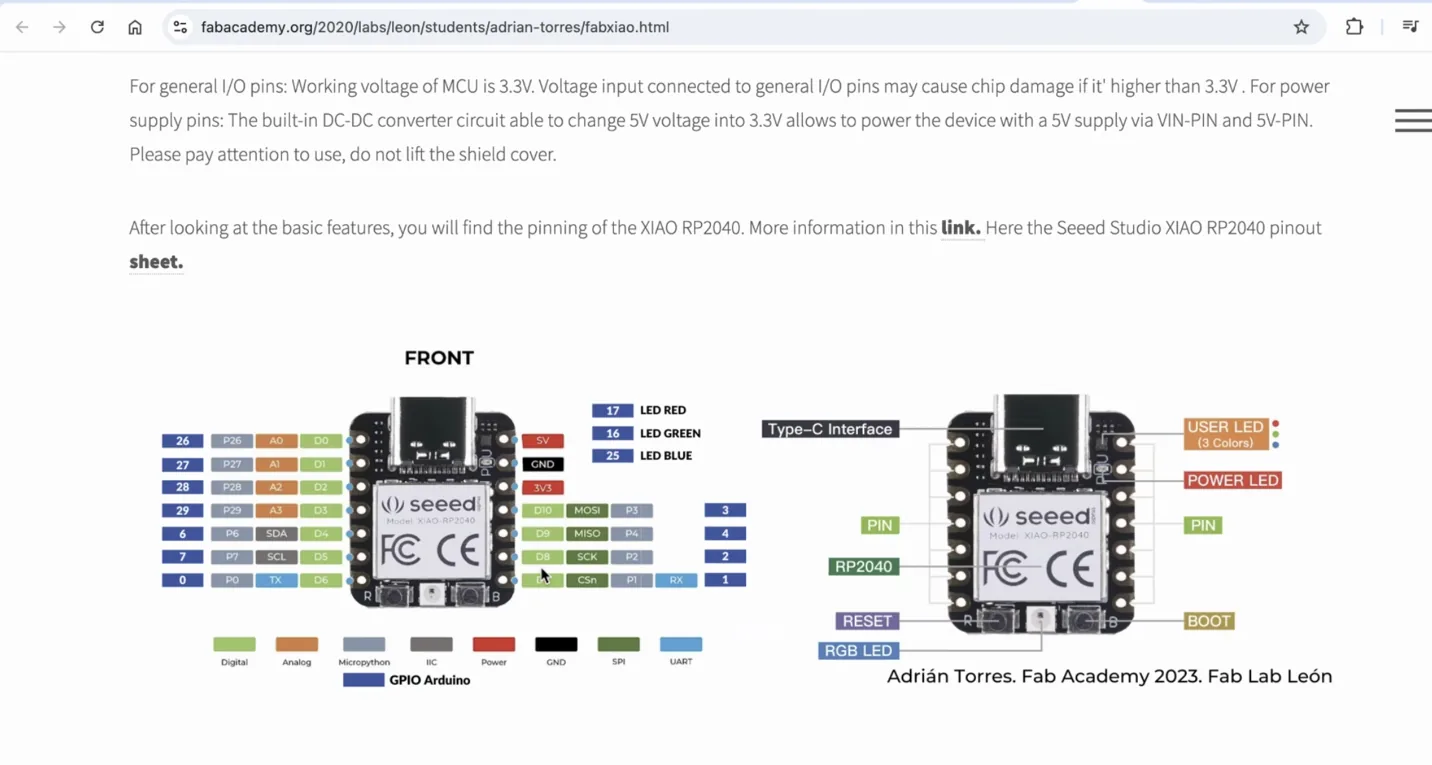
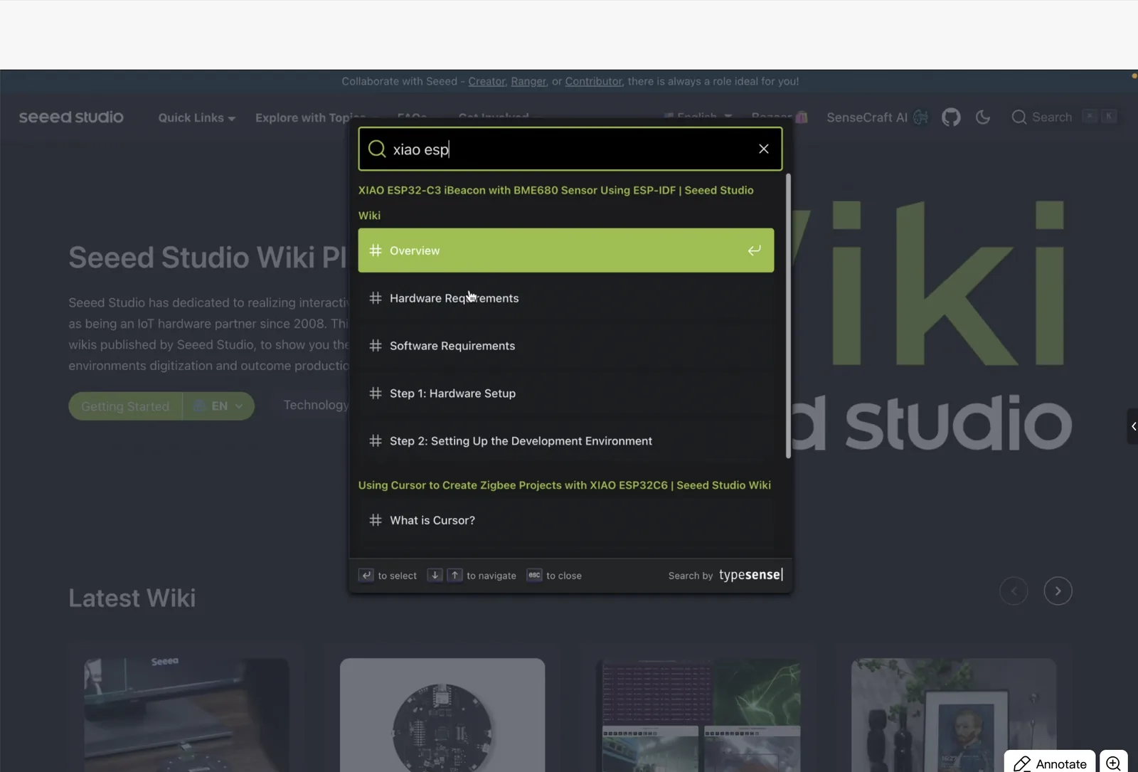
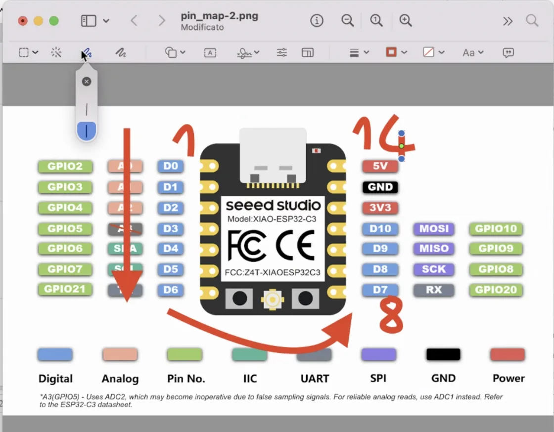
I used Adrian Torres's Fab XIAO project and the official XIAO ESP32-C3 documentation as references. I compared the board pinout, the schematic representation, and the real physical layout to understand how the pins should be mapped.
- Adrian Torres - Fab XIAO reference
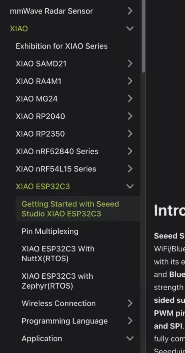
- Seeed Studio XIAO ESP32-C3 documentation
- Another XIAO-based board reference
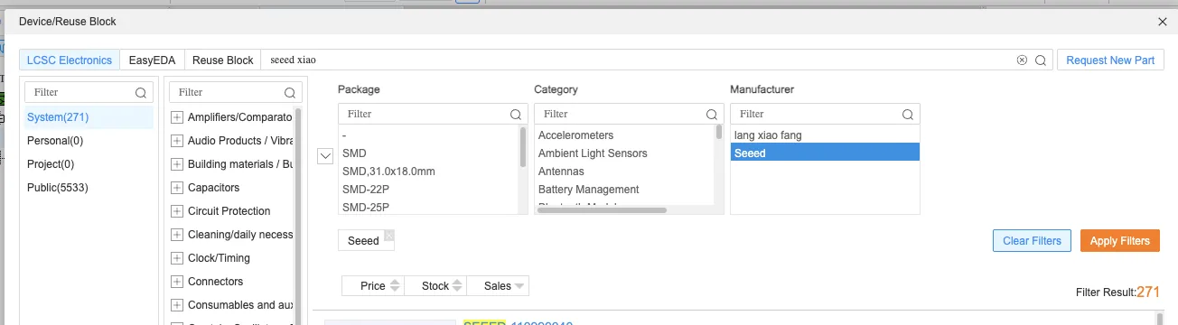
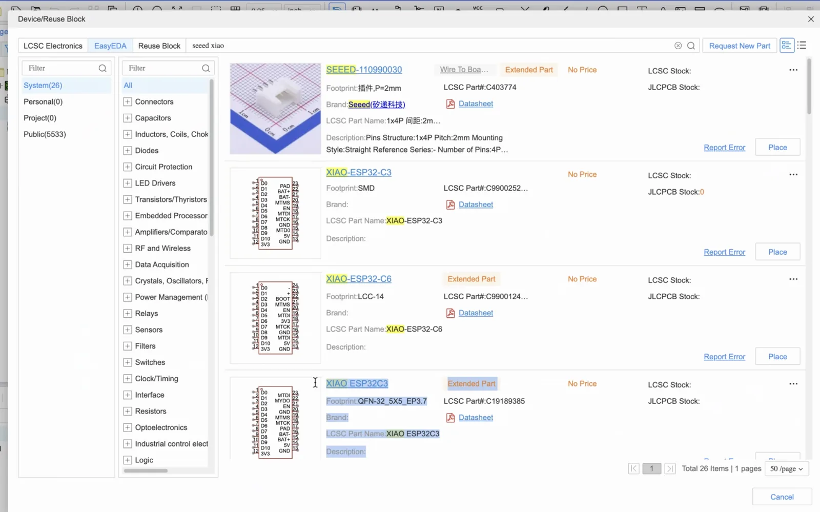
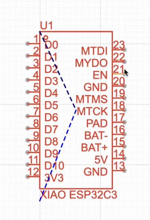
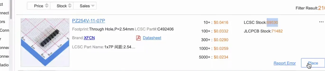
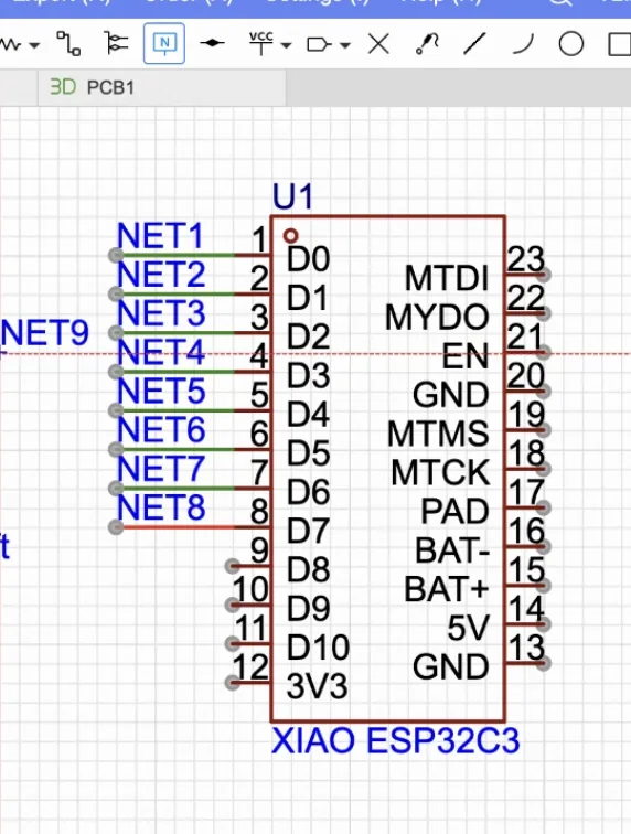
First, in electronic design, we can start from placing the actual microcontroller, in our case it is ESP32 XIAO C3. We can search for this electronic component using the brand name, the ship name, or company name because it's unique, such as "seeed".
Also, for one chip, we can see different examples of the electronic components' placement and with different links or providers who made it. Different links can contain different packages for this specific component. Also, I heard that the Chinese version of EasyEDA contains more electronic components, so when on the schematic it can look the same, when we can generate a PCB or 3D view, some features can be mixed. It's always good to compare the pins from the layout with the official documentation to count the number and to see the order.
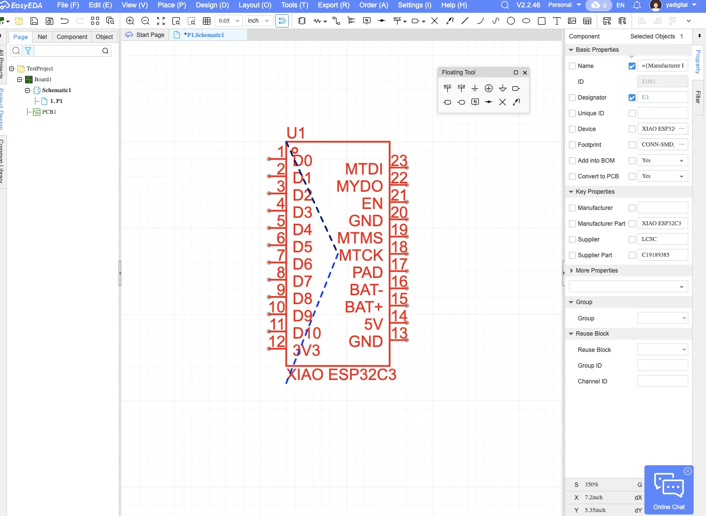
The naming of the pins happens in a counterclockwise direction, usually from the top left corner in the schematic. The real picture can be not the same as it looks, because some pins can be behind the board. It also can be demonstrated in a 2D schematic view, as in our case we see it, XIAO ESP32 C3.
Building the Schematic First
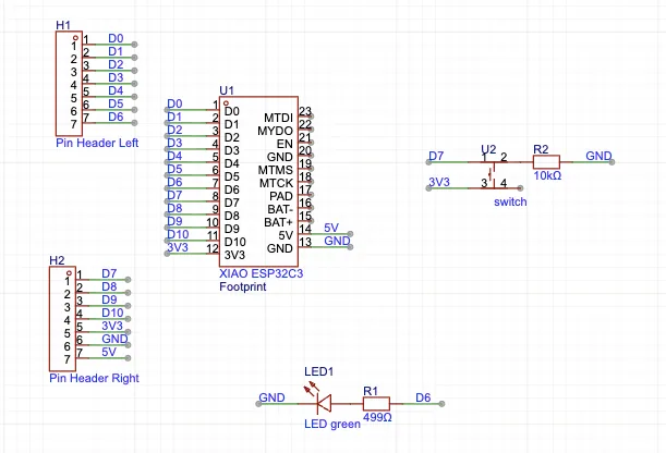
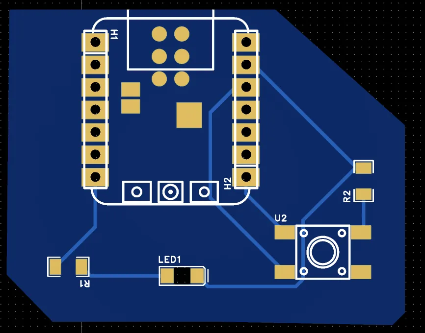
A PCB in EasyEDA starts from the schematic. I first placed the XIAO C3 component, then generated the PCB from it and continued editing only through the schematic whenever I needed to change the logical connections.
When PCB view is generated, we also can generate 2D and 3D view of the board. There are icons 2D and 3D for generating the graphics based on PCB.
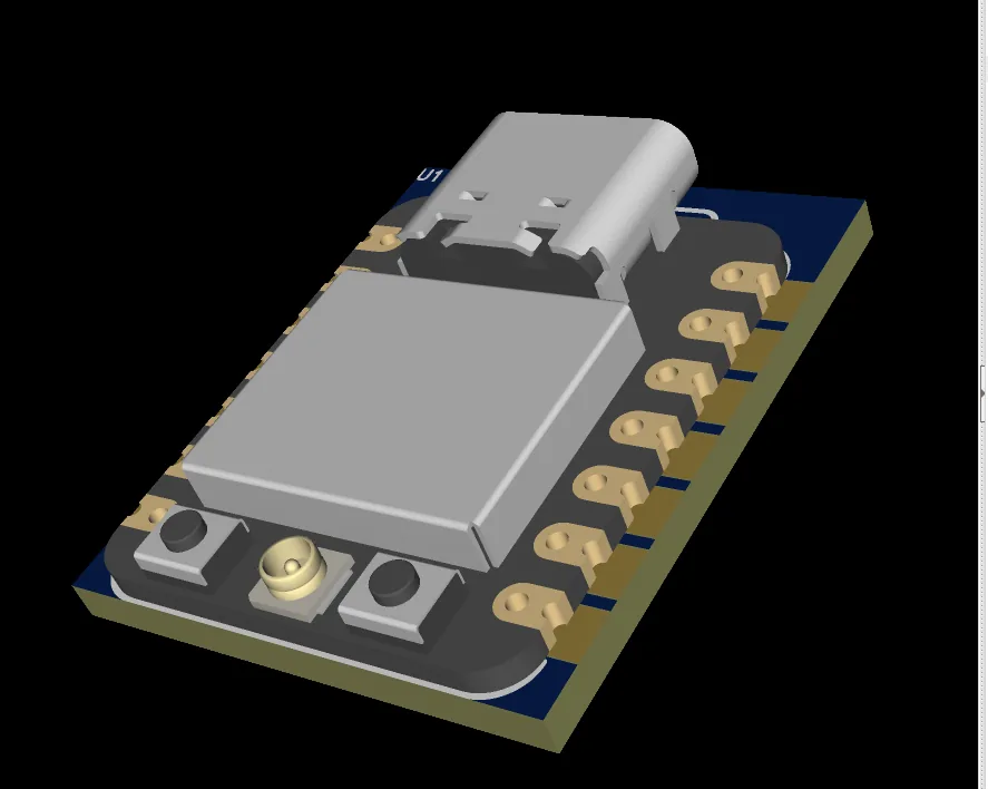
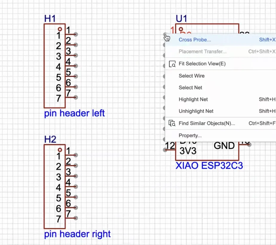
The next step - to add pin headers. Because I wanted to support the XIAO footprint, I needed a one-row, seven-pin header with 2.54 mm pitch. This standard pitch is a common electronics connector size.
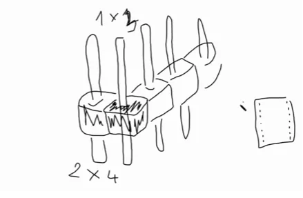
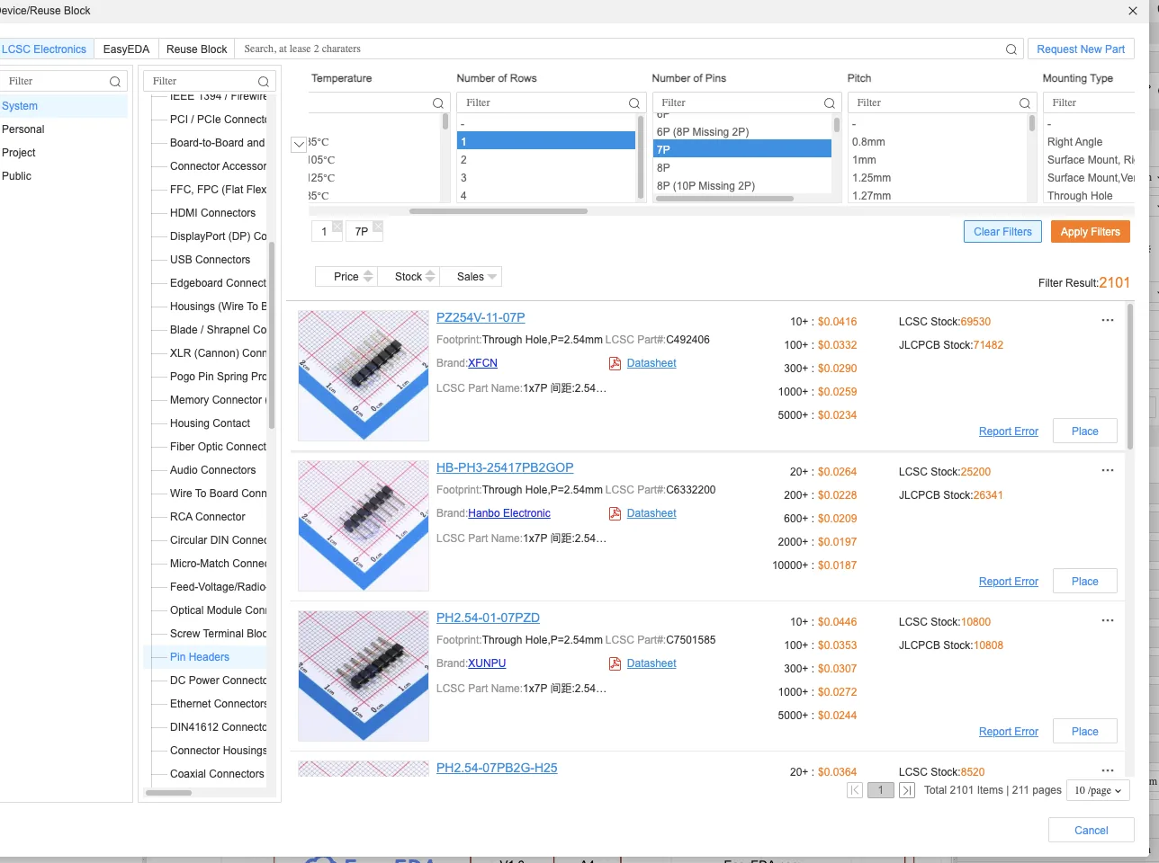
By pressing Add company and icon, we also can use a filter and choose "Connectors" - "Pin headers" section In the EasyEDA library, we can find different types of headers. In this case, we need a one-row, seven-pin header with 2.54 mm pitch. This standard pitch is a common electronics connector size.
After placing a component, we can rotate it, Flip it, move it, and position on our canvas as we need for our base design.
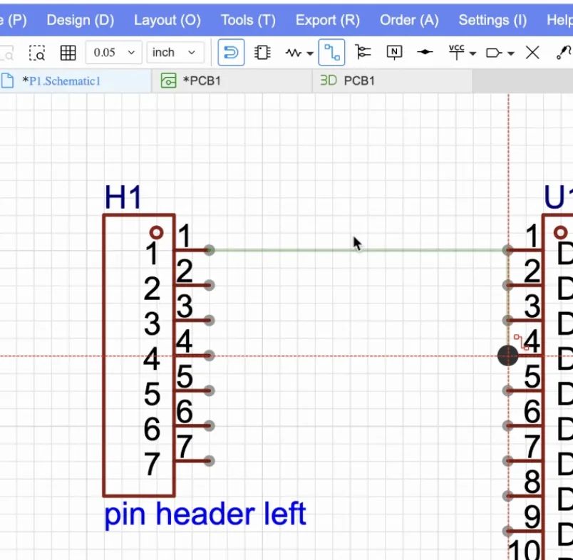
I tested two connection methods. The first was drawing wires manually. By pressing the icon with lines between two squares from the menu. Also, it's possible to move the whole pin header component and touch the pins from the shower component, then move it back, and all touched pins will be connected. he better method was using unified net names, because the schematic stays cleaner and the logic is easier to understand. In the EasyEDA, we can name the nets by pressing the net name icon and then typing the name.
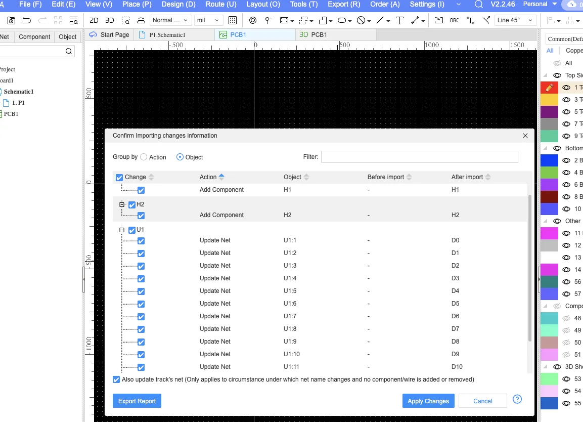
After finishing connection and naming the pins, we can generate the PCB view again. Then it will be a dialog
that says a new connection was found, and would we like to apply changes. After applying changes, the connection
will be established, and we can see it on the PCB and 3D view.
Matching the Footprints
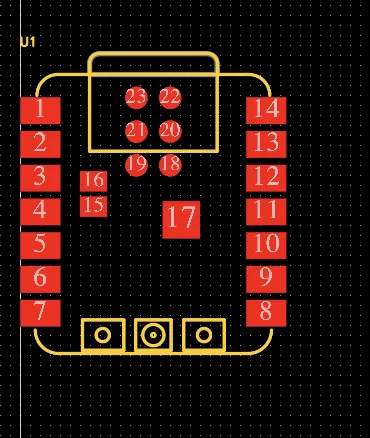
When I first generated the board, the header positions did not match the actual XIAO board location. I had to compare the footprints against the official documentation and then move or modify the footprint so the board would align with the real hardware.
For best practice, we can find the official footprint from documentation and use it to place the microcontroller on the PCB board. For the current case, it was a bit complicated to find the right footprint for Xiao ESP32-C3, so I just moved it manually.
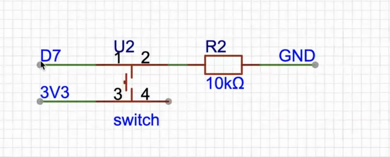
Adding an LED and Button
To satisfy the input/output requirement, I added an LED and a pushbutton. For the LED I also added a resistor as a current-limiting resistor. I used 1206 SMD components, because they are large enough to handle more comfortably during a first board design and later soldering.
It's useful to check more details about the existing schematic from Fab-Xiao and also to understand how the button actually works for better connection.
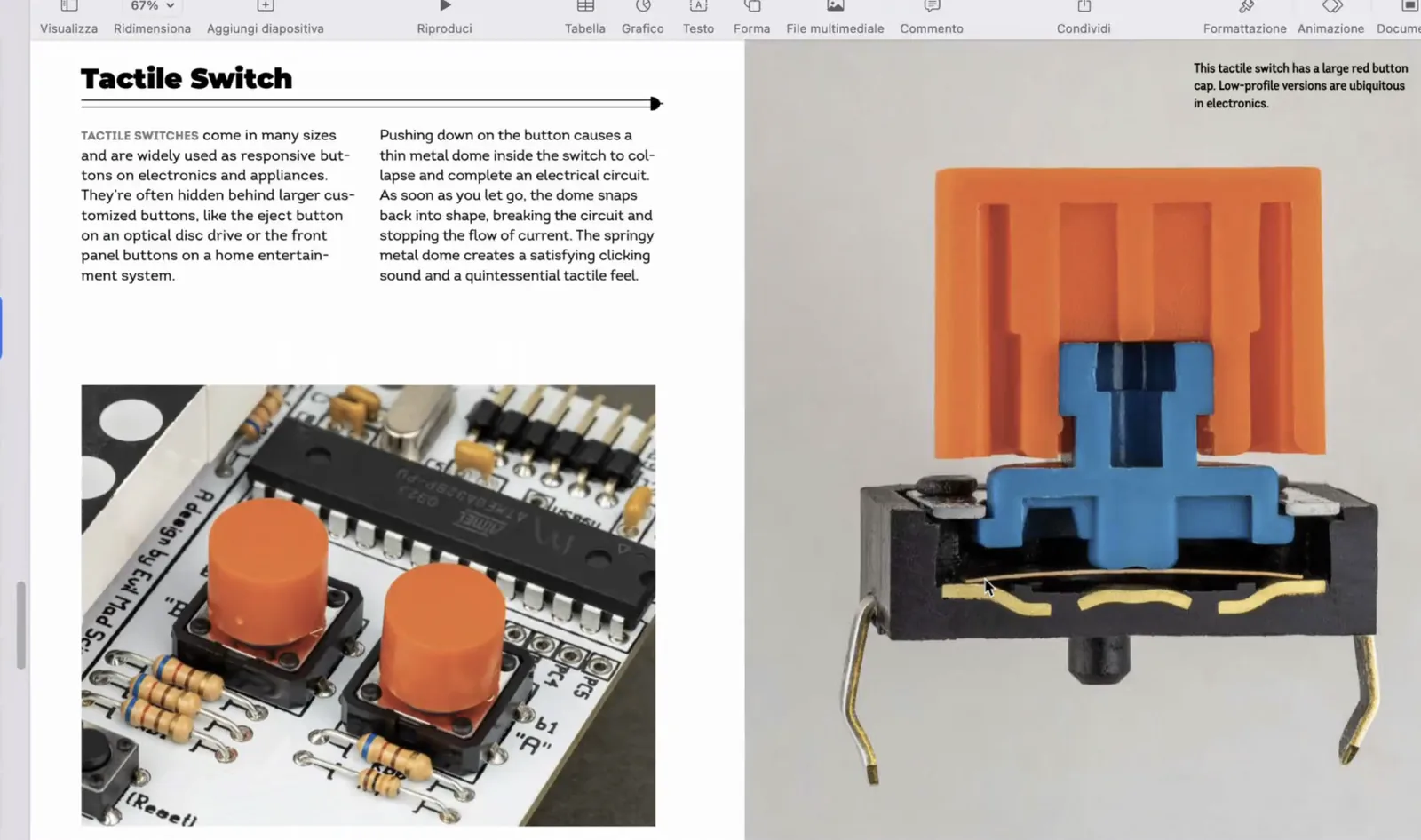
The button connection needed more attention, because it can easily create a wrong or unstable circuit if it is wired carelessly. I followed the reference logic and kept in mind that the XIAO board works at 3.3 V, so the external circuit should also stay within that limit.
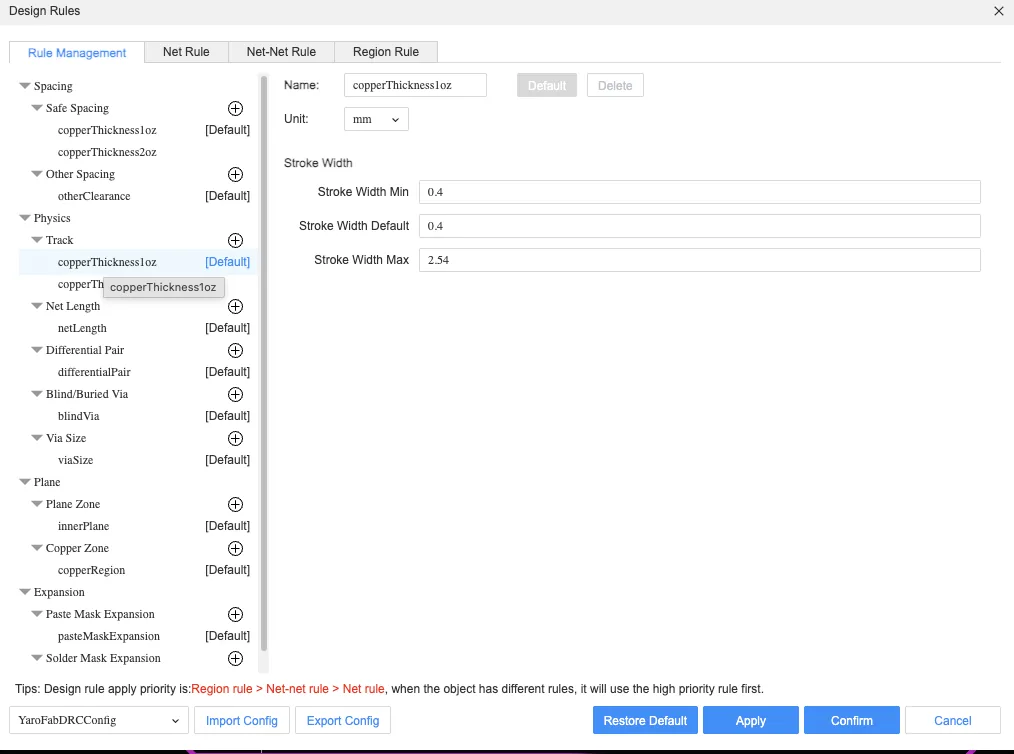
Design Rules for Milling
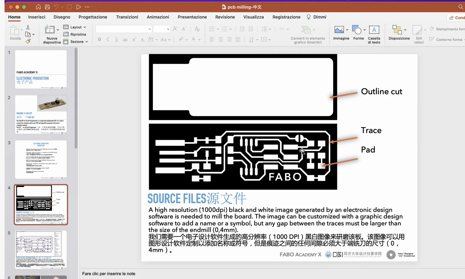
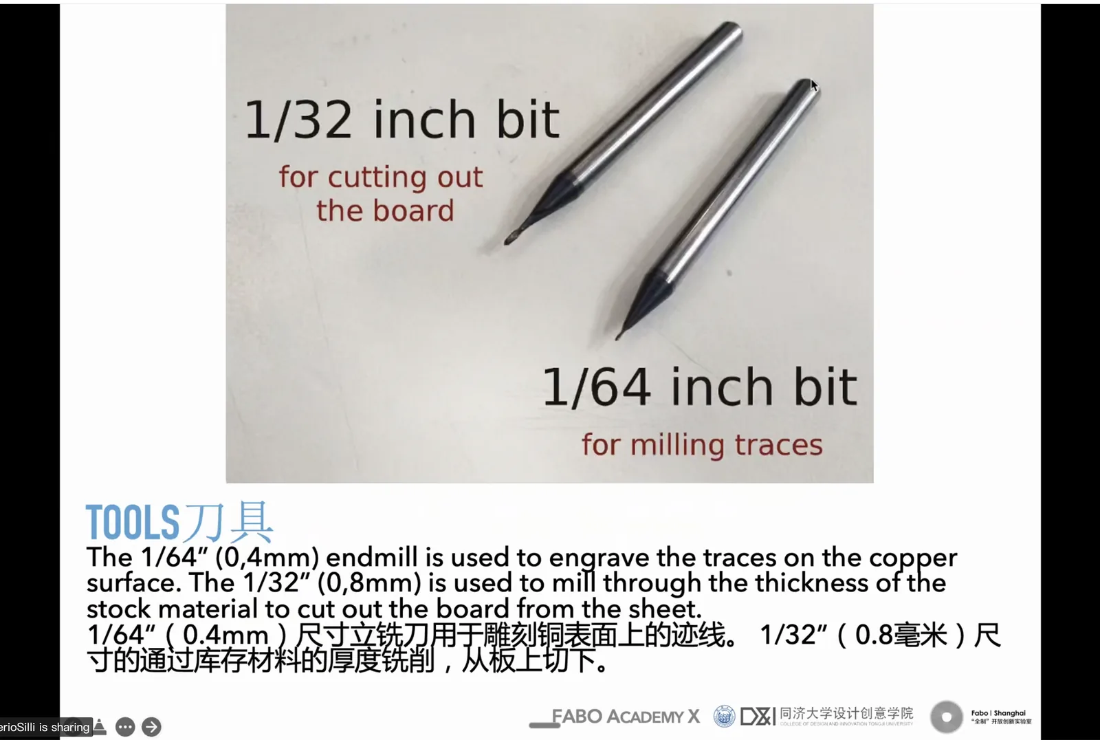
After the functional schematic was ready, I shifted to fabrication constraints. For PCB milling I needed to think about the two exported files, the board material, the milling bit diameter, and the minimum spacing between pads and traces. For future export, we will need Outline cut PNG file and traces PNG file. Outline cut PNG file will be used for the board outline, and traces PNG file will be used for the copper traces. Later on, we will use tool path generation software for PCB milling. For this case, we are about to use two end mills: 1. 1/32 in. bit for outline cut 2. 1/64 in. bit for traces and pads It will be two jobs for the CNC machine, and we will need to change end mills.
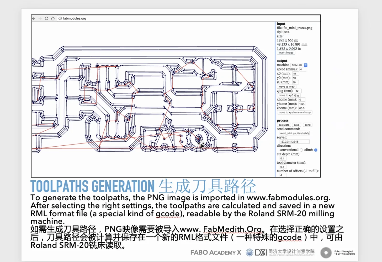
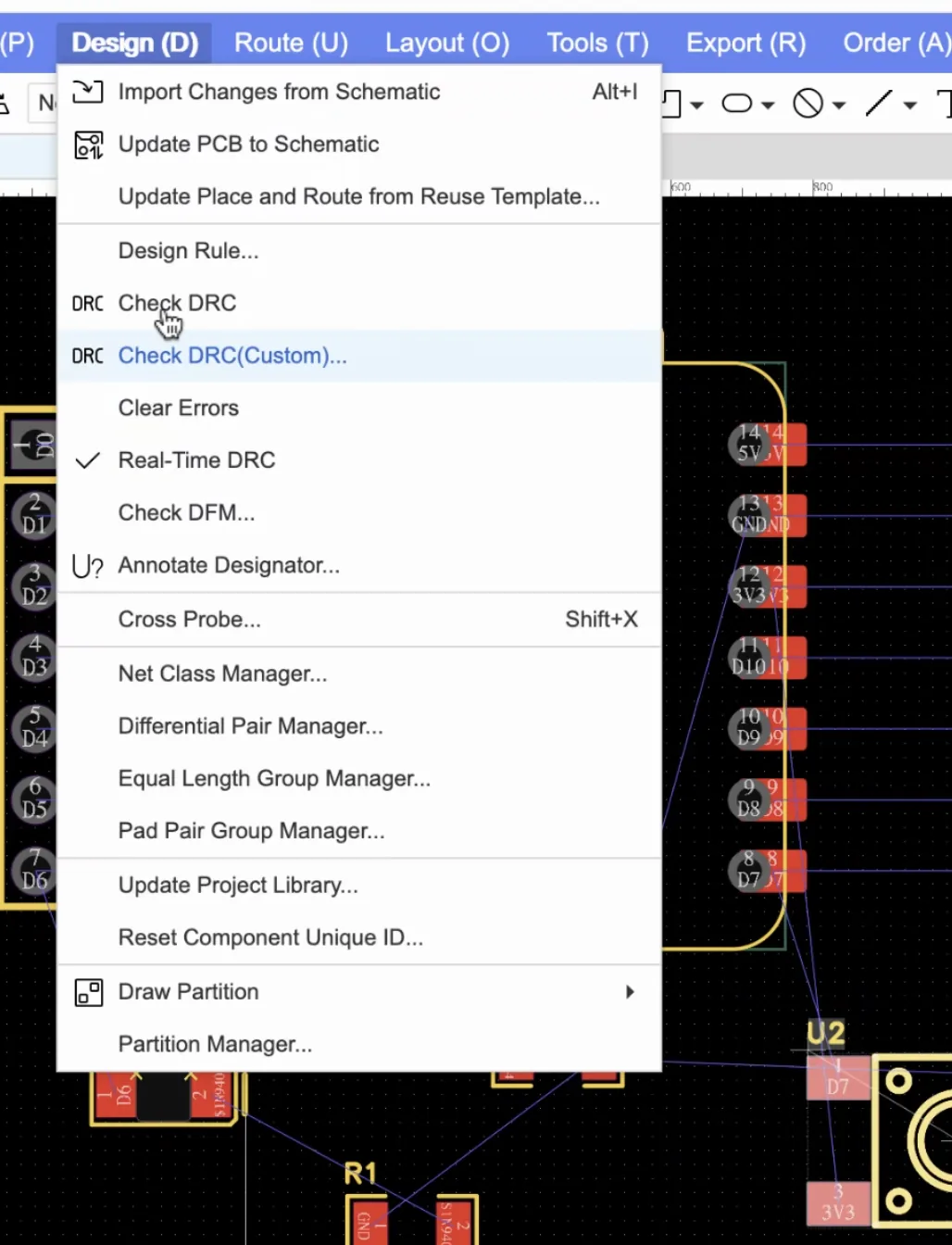
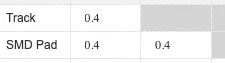
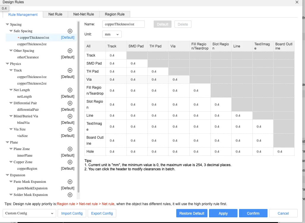
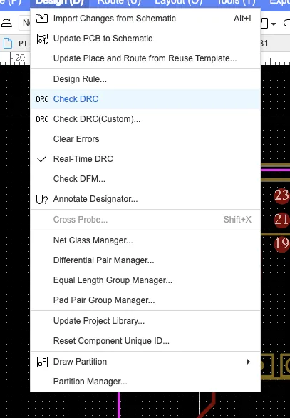
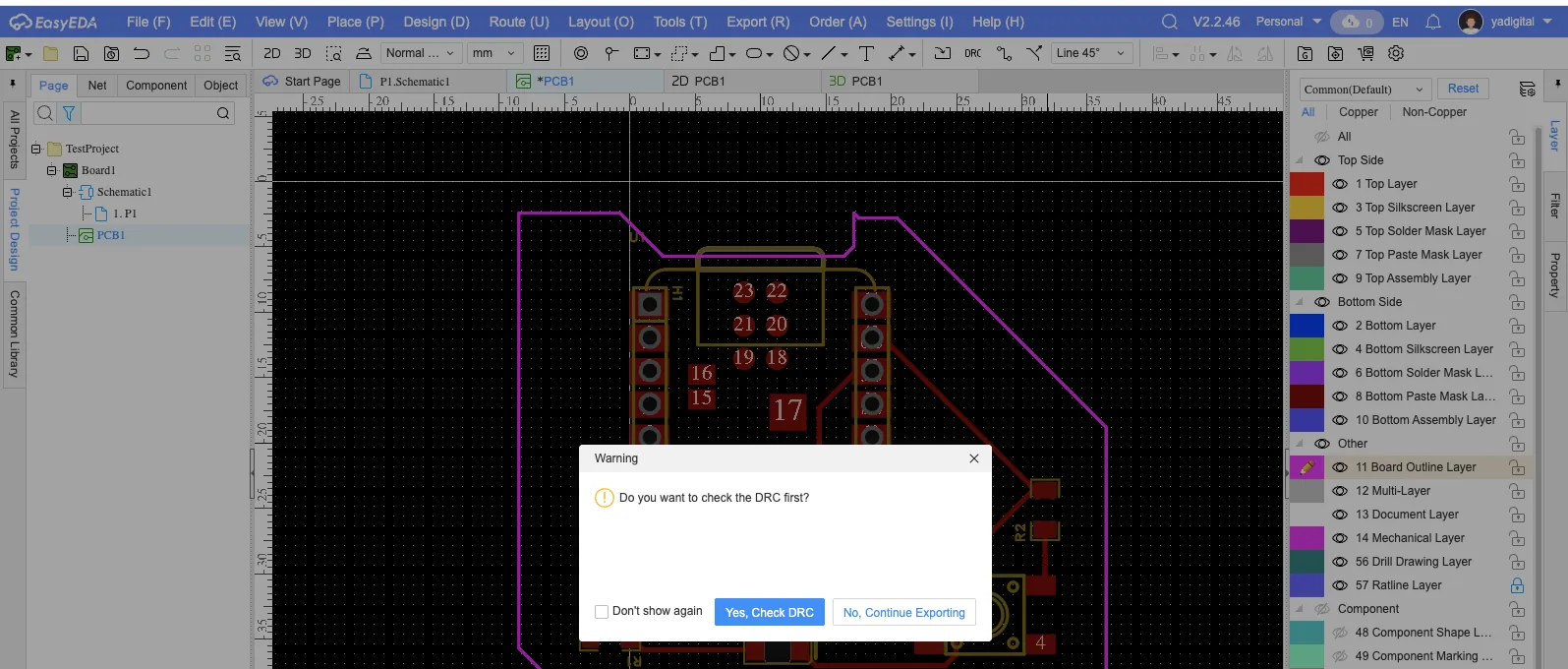
Before exporting in metadata, we need to check design rules, and it's possible from the easy EDA environment. Based on the milling constraints, I used 0.4 mm as a safe value for spacing and treated that as the minimum practical clearance for this beginner board. I also reviewed stroke width and track settings so the board would be easier to fabricate. Because it's my first experience and due to the time issue, I will just add a 0.4 constraint for each possible dimension.
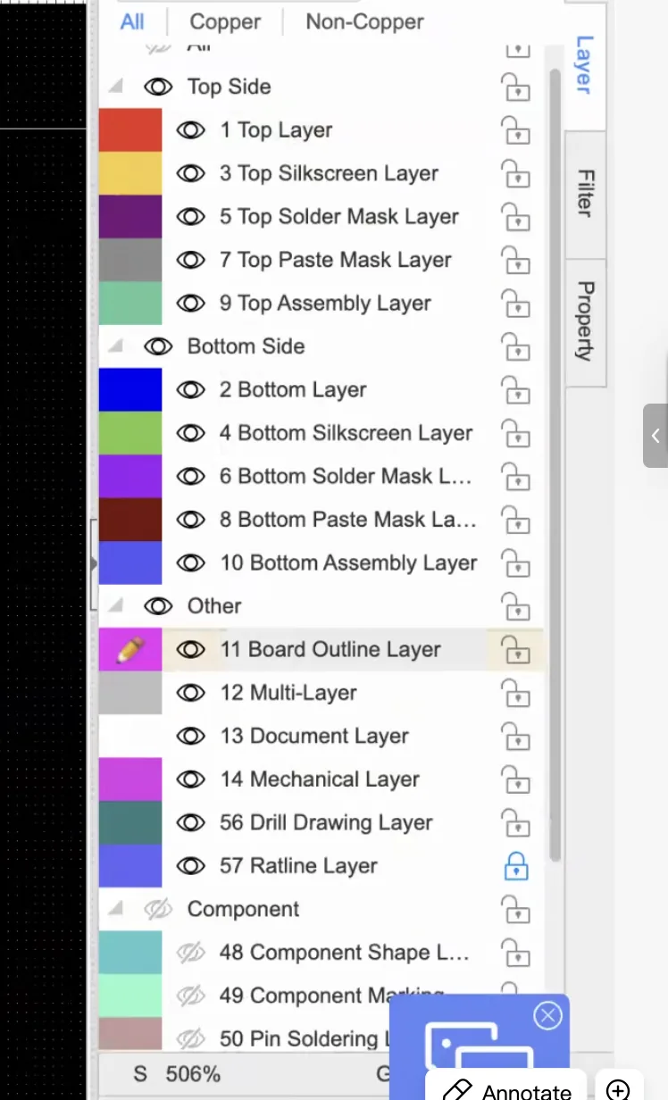
For drawing board outline, it's better to keep visible only two layers because it's a simple board: only traces
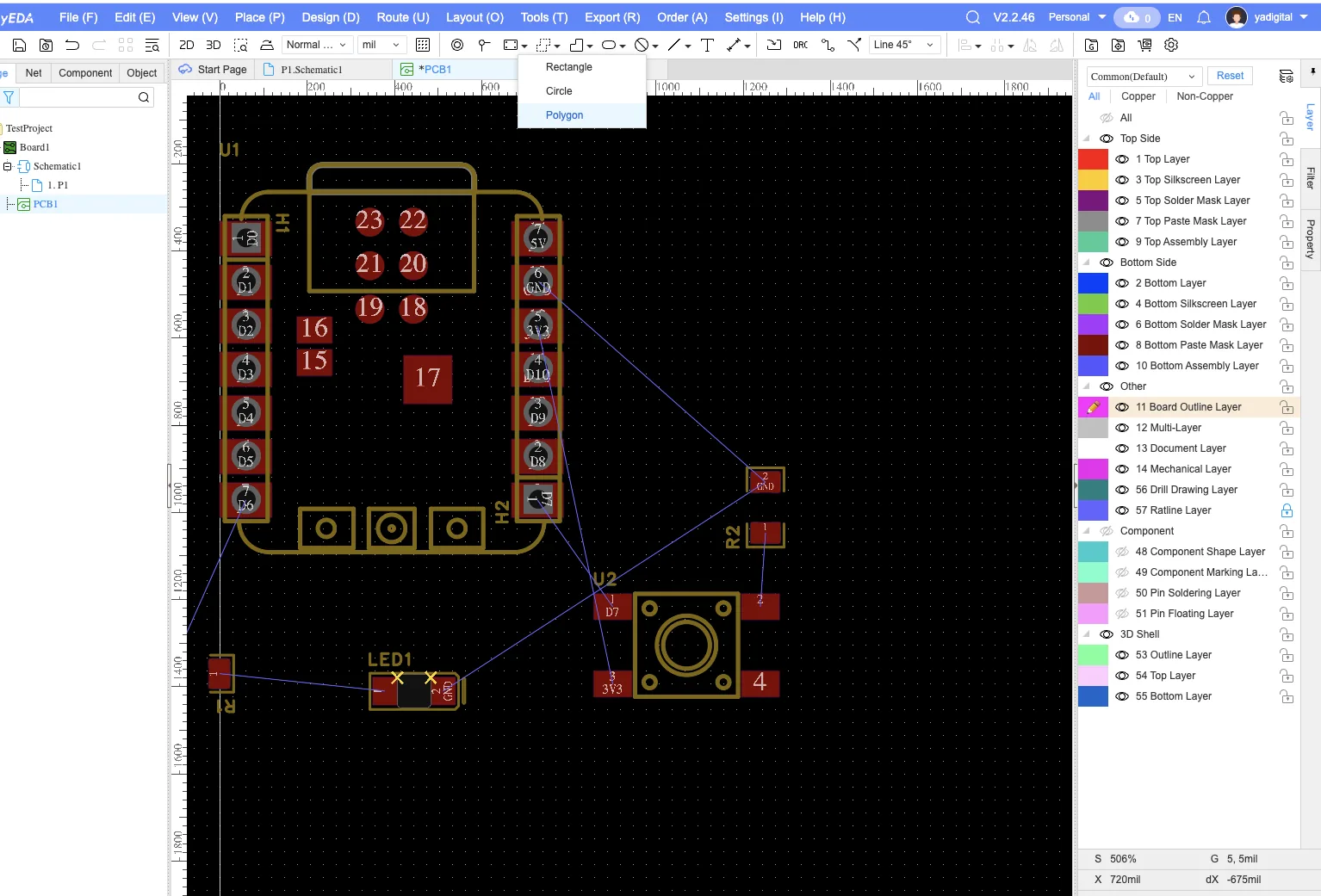
and only outline. Also, for the board outline, it's possible to use: Rectangle shape, Circle shape, Polygon shape
For a cool design, it's possible to export DXF format with some custom design.
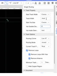
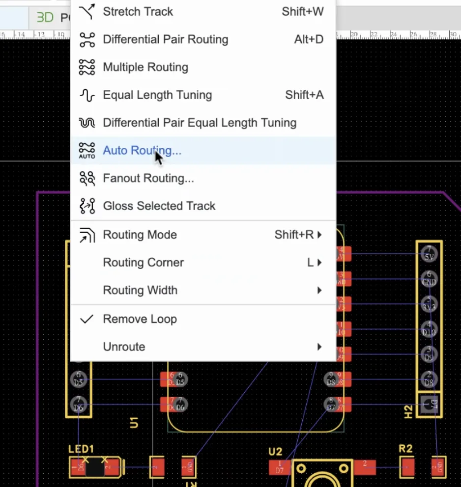
Routing the Board
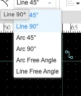
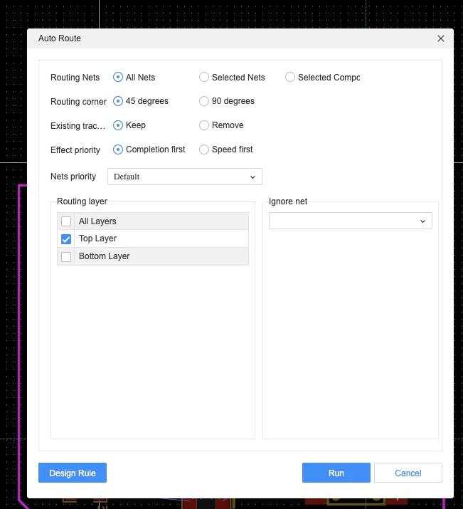
While routing, I kept the traces as far apart as possible and avoided sharp 90 degree corners. I changed the working width to 0.4 mm and used autorouting as a starting point, then reviewed the result manually to make sure the paths were still reasonable.
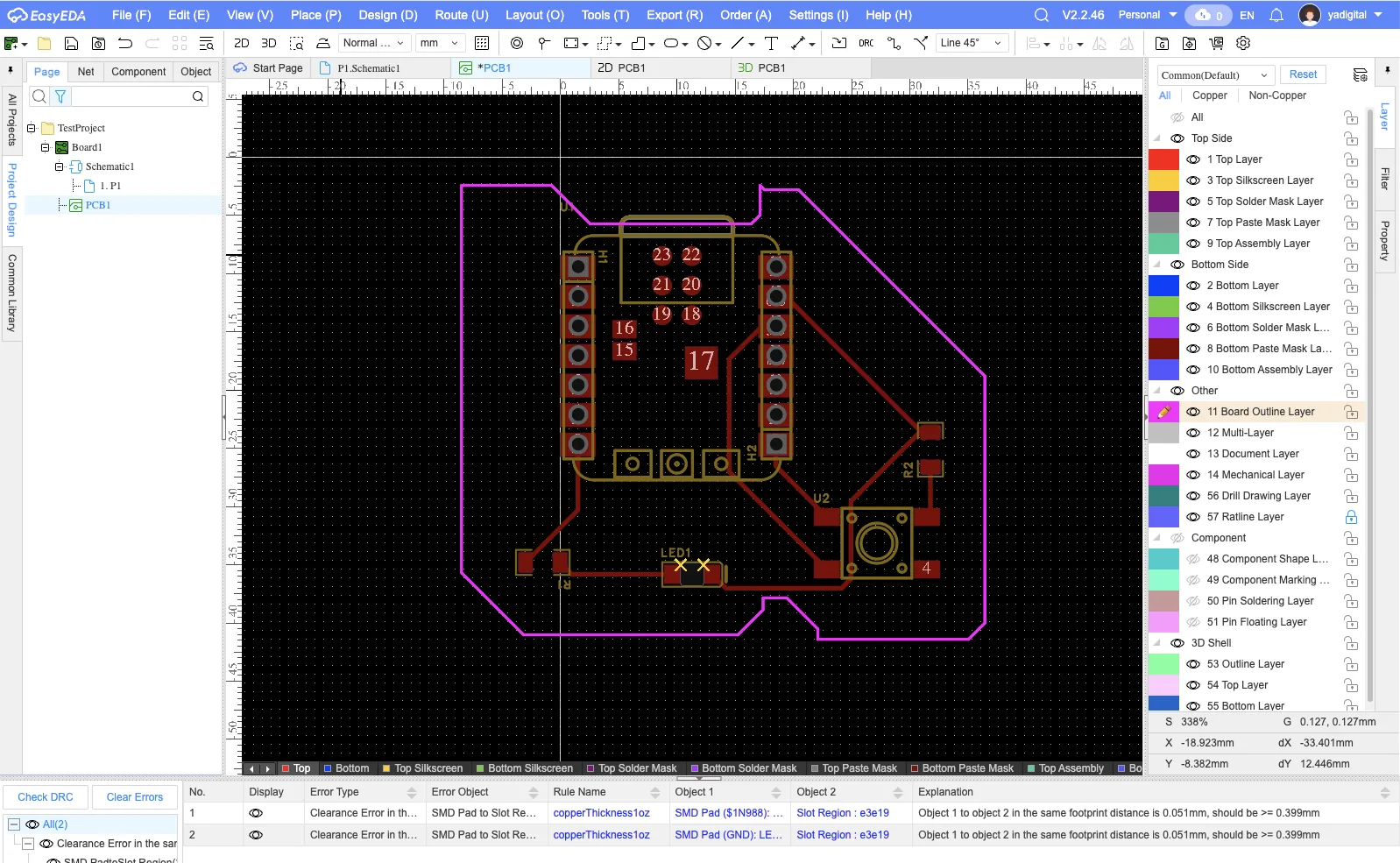
DRC, Export, and Final Board
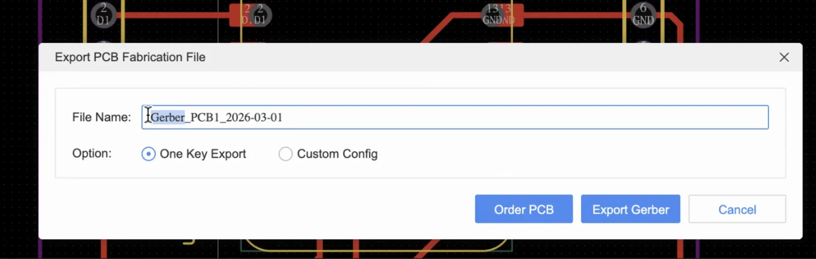
Once the board looked complete, I ran design rule checks and then exported the fabrication data. EasyEDA reported two errors, but these were related to the LED setup and not to the overall board layout. The production output is a Gerber package that can be sent to a PCB manufacturer directly.
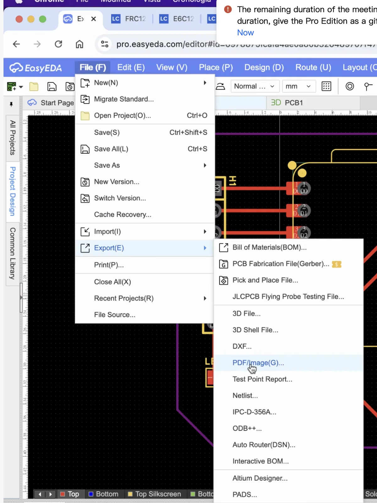
For future milling, we need to export a gerber file, and then we can use it for generating PNGs and toolpaths.
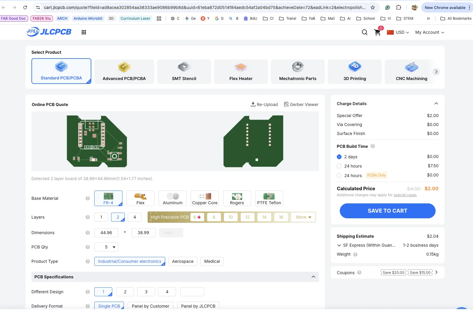
It's possible to order the board already milled on FR4, but for this case, I would like to do it by myself on the future classes. I will order another board from the board house. For this case, it's just needed to upload the Gerber file, select the amount of boards and other options, and then pay. And after several days, the board will arrive at my home.
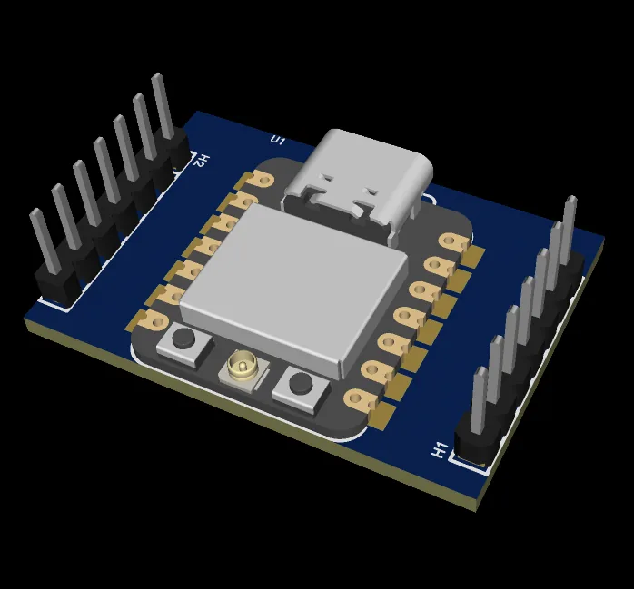
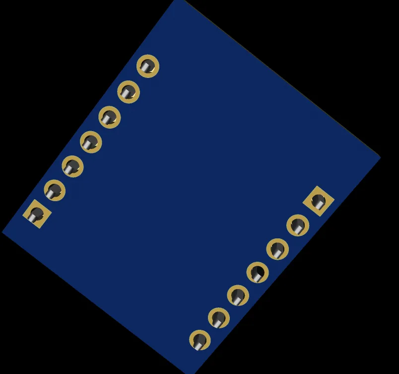
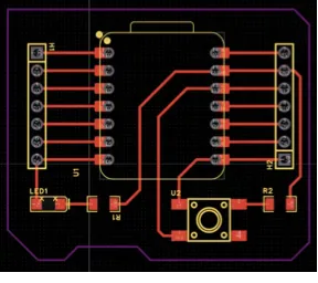
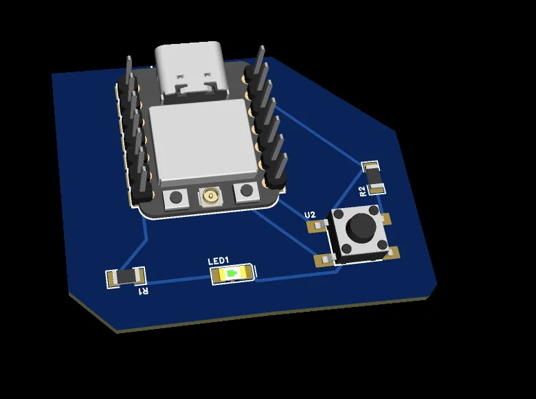
My final schematic, PCB view, 2D and 3D design
Reflection
The main thing I learned this week is that electronics design is not only about drawing a board shape. The real workflow starts from the schematic, then moves through footprints, placement, routing, fabrication rules, and final export. I also learned that documentation and official pinout references are essential, especially when the schematic symbol and the physical board layout do not look the same.
KiCad and Eagle are still worth learning, but for this first pass EasyEDA helped me understand the sequence more quickly. The most important practical lessons for me were using named nets, checking footprint dimensions against documentation, staying conservative with clearances, and always running DRC before export.
Files
Download the fabrication output for this board here: