Week 8
Assignment - Electronics Production
-
Group assignment:
- Characterize the design rules for your in-house PCB production process: document the settings for your machine.
- Document the workflow for sending a PCB to a boardhouse
- Document your work to the group work page and reflect on your individual page what you learned
-
Individual assignment:
- Make and test a microcontroller development board that you designed
From Assignment Details.
Group Assignment
Design Rules for PCB Production Process
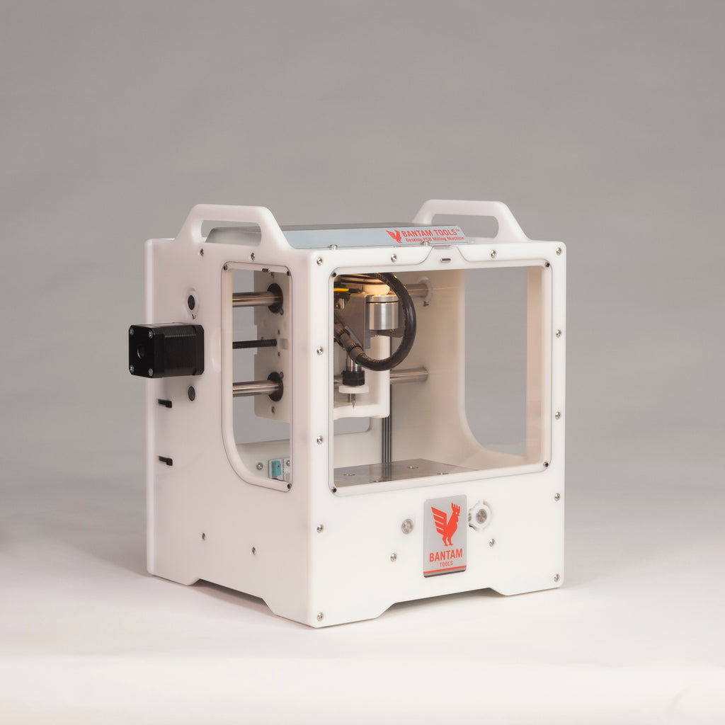
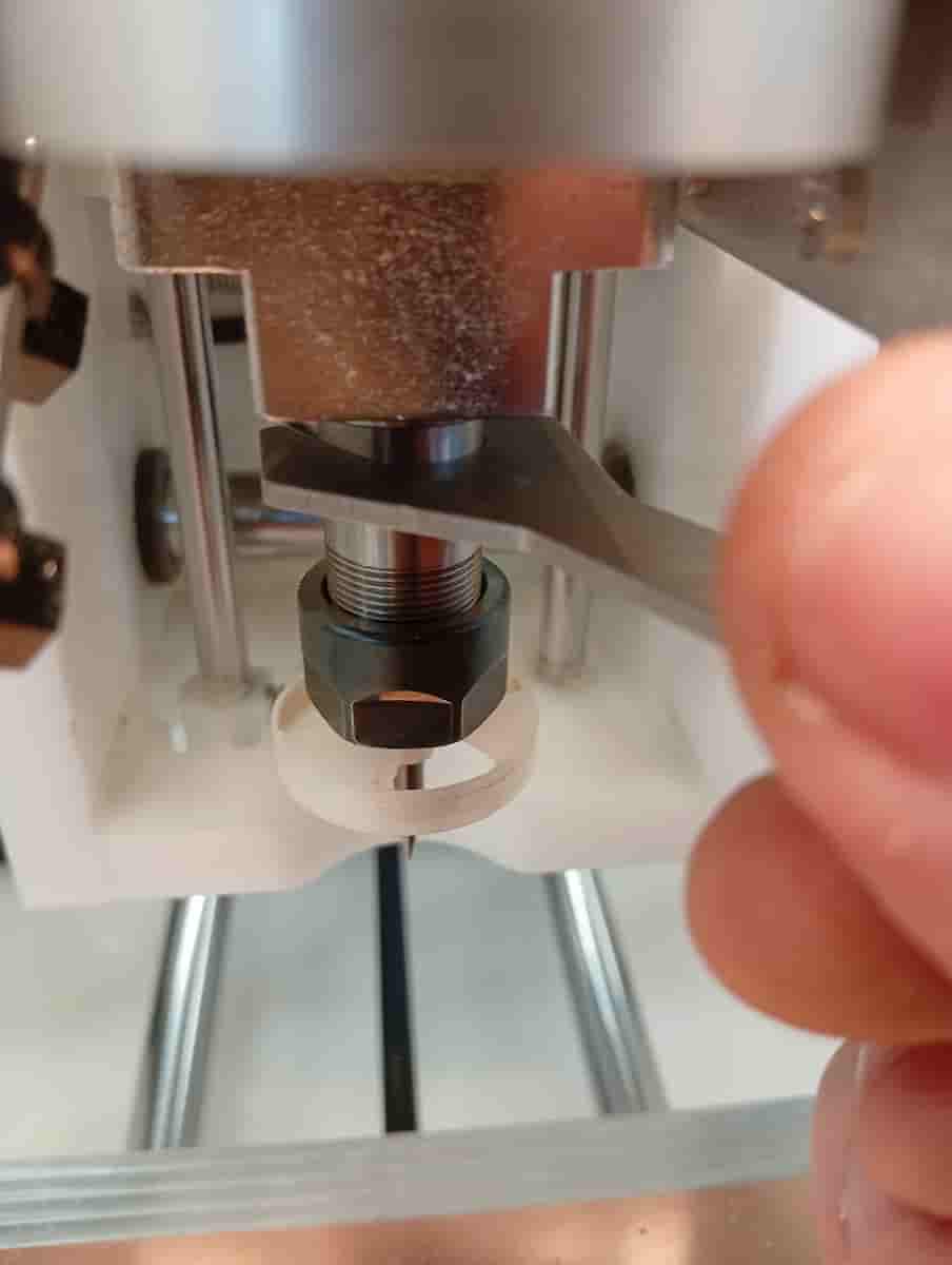
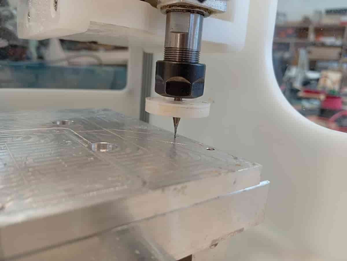
Based on the Bantam PCB Mill and the 1/32” flat endmill and the 0.003” engraving bit.
| property | units | 1/32” endmill | 0.003” engraving bit | 0.005” engraving bit |
|---|---|---|---|---|
| diameter | mm | 0.794 | N/a | N/a |
| point | mm | 0.794 | 0.076 | 0.127 |
| taper angle (total angle) | ° | 0 | 30.475 | 29.998 |
| feeds | mm/min | 1100 | 350 | 350 |
| speeds | rpm | 27500 | 16500 | 16500 |
| plunge rate | mm/min | 381 | 200 | 200 |
| pass depth | mm | 0.8 | 0.25 | 0.25 |
Test for track/trace width
I decided to try Neil’s test.
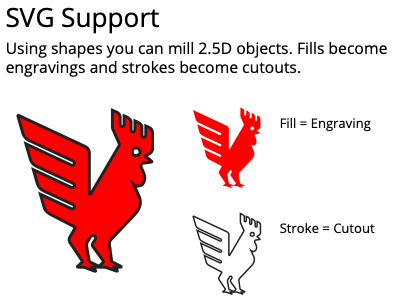
Bantam’s software takes .SVG but not .PNG. So I traced the trace test in Inkscape.
This is the way to prepare the .SVG (Fill (Red?) = Engrave; Stroke = Cutout). Free version cannot use the “Advanced SVG Workflow”. One missing feature is internal cutouts, you have to save multiple .SVG files and set them up together. Each file can take a Cutout Placement setting of Outside/Center/Inside. You have to use a stroke thickness, so for the 1/32” endmill, I made the strokewidth 0.82 mm. You can select Invert: Yes, within Cutout, which would be a nice way to remove the outer copper if you were worried about shorting to it.
Note: Units have to be in Inches in Document Properties. (File > Document Properties).
Which I applied as:

Download: linetest_inkscape_traced.svg
Results
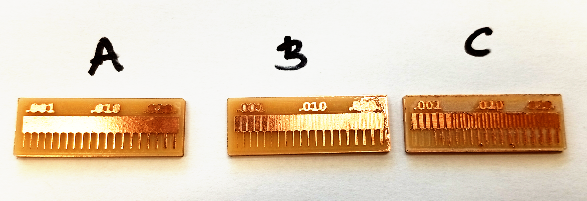
- A was 1/32” flat endmill only
- B was 0.005” engraving bit and 1/32” flat endmill
- C was adjusted by -0.2mm i.e., (board thickness back to 1.6mm), using 0.005” engraving bit and 1/32” flat endmill.
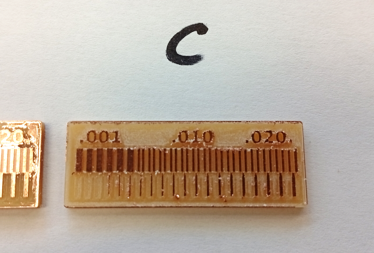
Definitely needs some deburring, but shows the capabilities of our milling machine
A result of SVG milling was that the machine never tried to mill tracks that were deemed to narrow in the CAM software. Eg., with the 1/32” flat endmill we’re just seeing ignored tracks. But that may be ok.
- Board uneven-ness. To mount my FR-1, I used double-sided tape and a mounting bracket. From the result, you can see engraving didn’t reach the corner of the second board. And I watch it go through all the toolpaths, just fly over that corner. I had done the touch-off on the metal bed. I assume that I measured the material thickness/tape thickness incorrectly. To remedy, I will change the Z-offset by 0.1 - 0.2mm.
My measured design rules are as follows:
| property | unit | |
|---|---|---|
| technology | - | pcb milling |
| trace (width) | mm | 0.100 |
| inch | 0.004 | |
| track (spacing) | mm | 0.175 |
| inch | 0.007 | |
| layers | - | ≤ 2 (with bracket etc.) |
| min text height | mm | 2.0 |
Sending a Design to PCB BoardHouse
I tried:
The price from JLCPCB was $5 + $23 delivery (1-2 days build time). NextPCB wanted $43. But allows you to specify Manufacturer components and position them to have it populated. I think to do that with JLCPCB, you may have to prepare it in EasyEDA and use parts from the official components’ library.
Centroid Files (NextPCB)
NextPCB accepts .Zip / .RAR / .xlsx / .xls. You can export this from your KiCAD PCB file, File > Fabrication Outputs > Component Placement, and specify the format as .CSV (This is what I did at least, but maybe .POS or .Gerberx3 ) You need to convert your .CSV as .XLSX or .XLS.
| *Manufacturer Part Number | *Quantity | Manufacturer(Optional) | Package(Optional) |
|---|---|---|---|
| etc. | etc. | etc. | etc. |
| . | . | . | . |
You need a BOM file that corresponds to your “Centroid File”, and this would take a little more time to make sure everything matches up and matches the KiCAD library.
Exporting from KiCAD
Go to File > Fabrication Outputs > Gerbers (.gbr)
And on the Gerber export window, click Generate Drill Files....
Running Software Tests
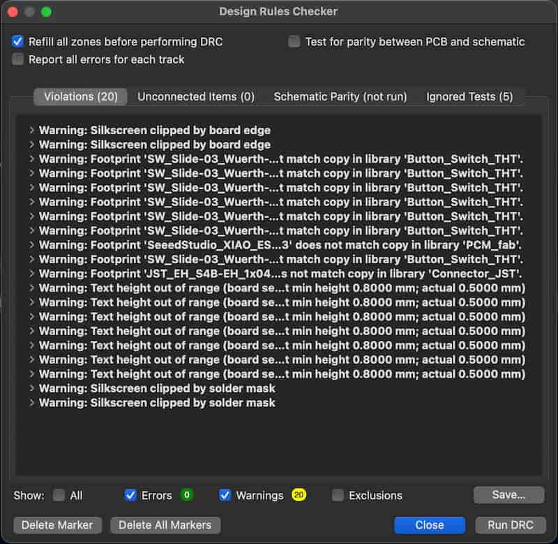
These errors are:
- Silkscreen runs over the edge of the board (has to in some cases - the ESP32 antenna and the right angle connector I designed for),
- Text to small (0.5 too small, minimum 0.8),
- Footprint does not match the linked file (I changed the footprint myself, do not need populated).
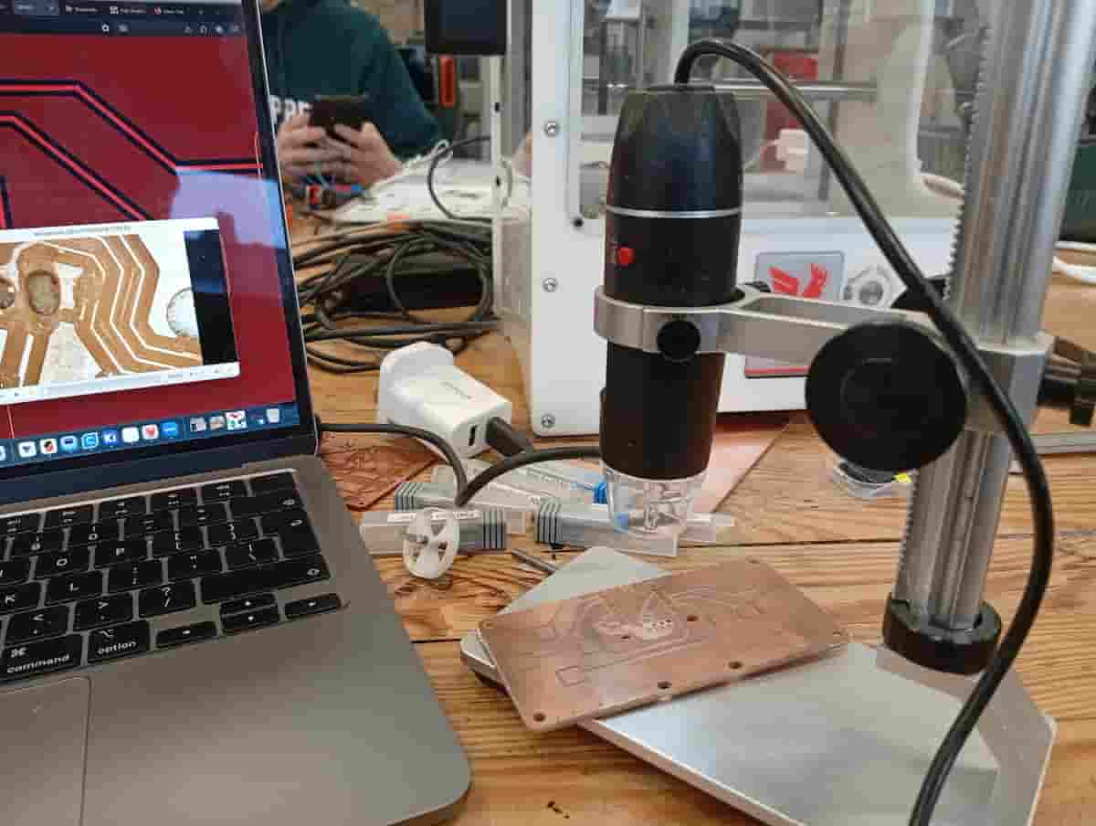
Individual Assignment
This week I made a QPad, by Quentin: https://quentinbolsee.pages.cba.mit.edu/qpad-page/ and updated from the one I designed in KiCAD in Week 6, that I hadn’t tested yet.
Before you start
Check the type of OLED screen you have! Order was GND - VCC - SCL - SDA, so no change needed fortunately! Thanks Carl!
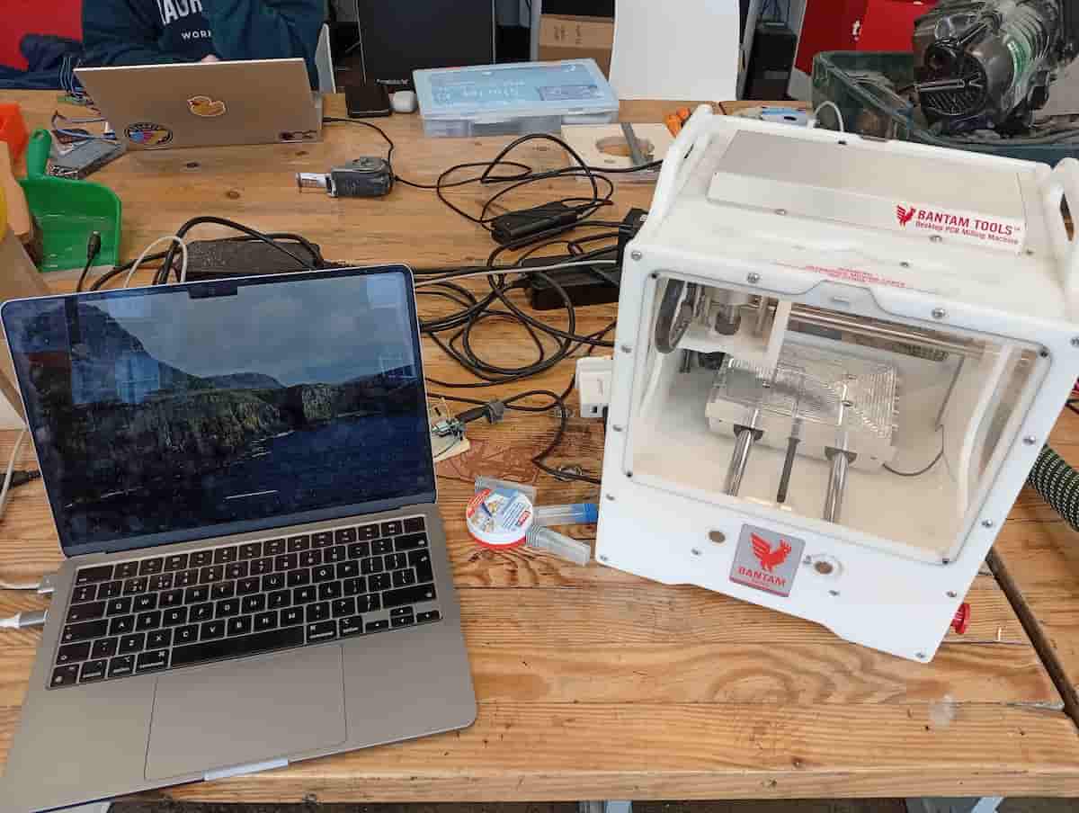
Equipment:
- Bantam Mill
- Solder Station (with Hot Air Gun)
- Tweezers
- Various Components
- FR4 (two sided copper)
- Flux
- Laptop (using Bantam Mill software)
- PPE, and extraction (Festool vacuum)
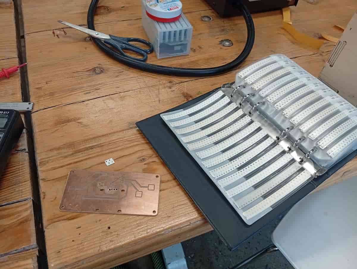
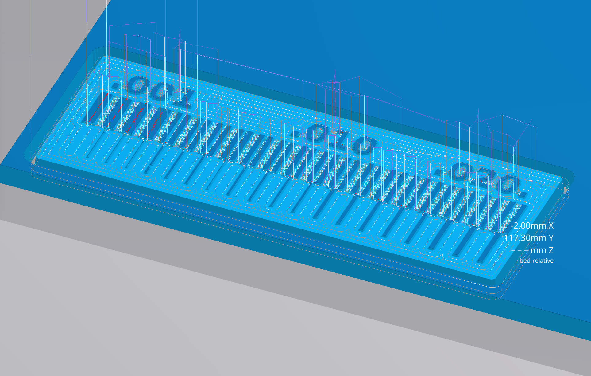
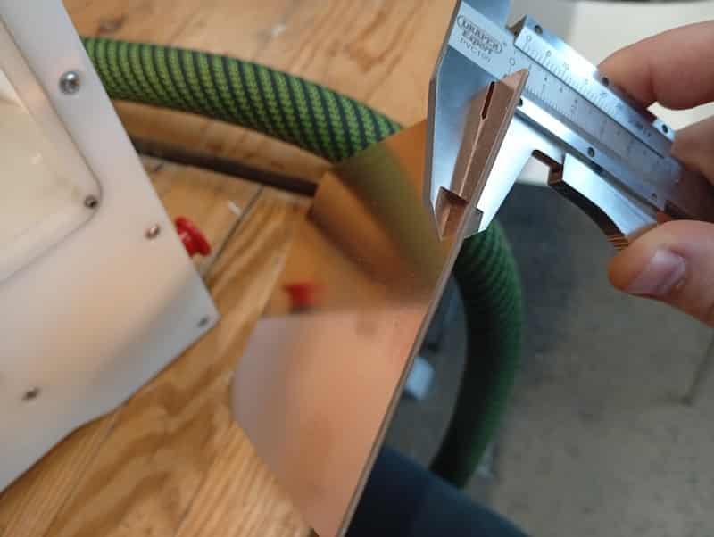
Attempt 1
Measured to be 126 x 101 x 1.6 mm. This is not including the sticky tape: 1.7mm.
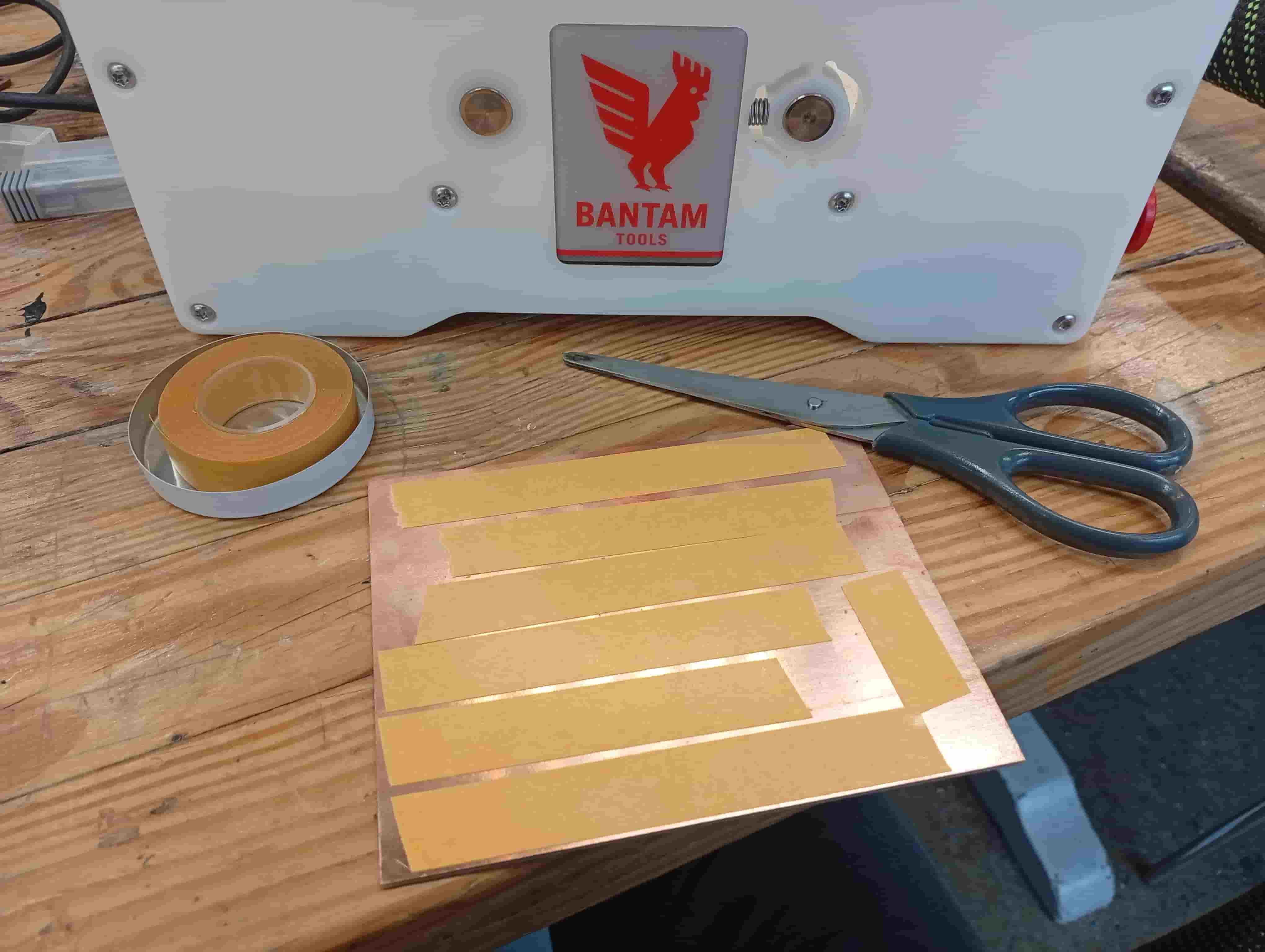
Stuck down the material with double-sided tape.
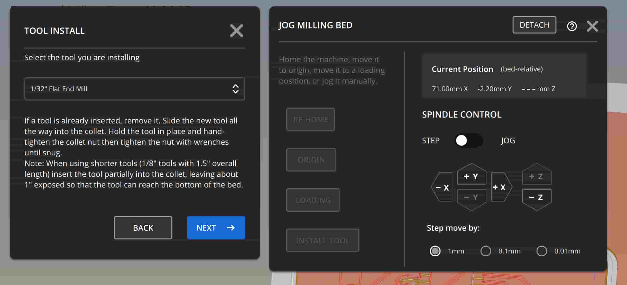
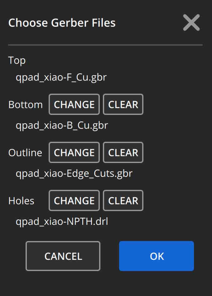
Go to File Setup, and New CAM to load your Gerber files.
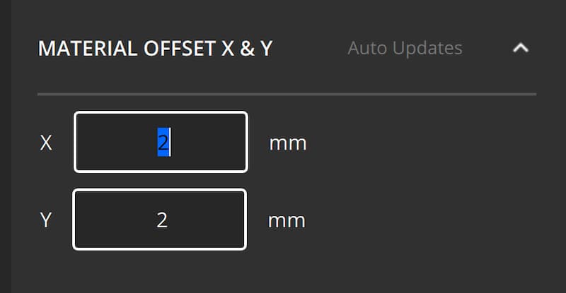
Offset by 2mm in X and 2mm in Y, but tool was 1/8” so the outer profile still cut to the edge.
Remember to Generate All Toolpaths again.
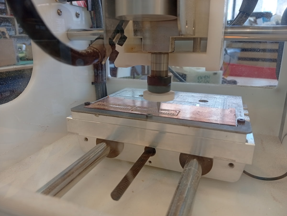
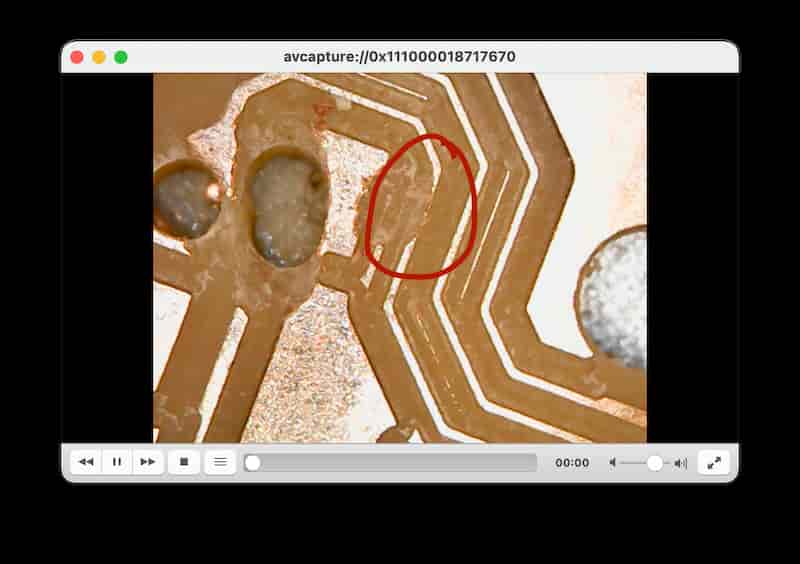
Result of attempt 1
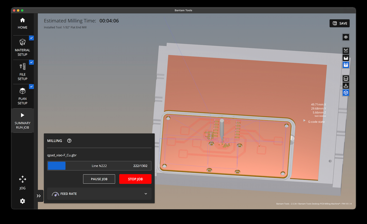
To cut, I selected Mill All, and activated the extraction. The tool lowered and spun up.
Initially it only cut the toolpaths for the 1/32” flat endmill, and paused. This was less than I expected. I stopped the Job, and changed the tool to the 0.003” engraving bit, which fit into the traces now. I changed to the 1/8” flat endmill for holes and cutout.
I didn’t notice that the render didn’t include throughholes for the OLED screen. To make the most of this test, I will try to make the holes with a dremmel and a 1mm bit. The pads are probably tight for this, so it’s not a good solution.
Attempt 2
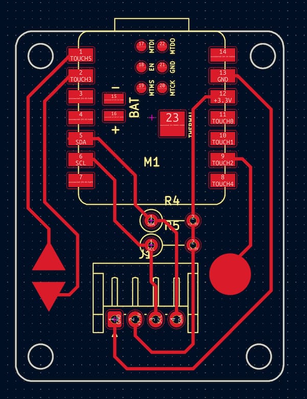
I decided to try make a generic breakout board à la Adrian’s Input Device Designs. This is the design I use also in Week 9, Input Devices and Week 10, Output Devices and Week 11, Networking and Communications.
Skip to KiCAD files…
I had to patch my wiring, because my i2c connectors on the BME280 board were
+/-/C/Don the OLED wereSCL/SDA/VCC/GNDand my board wereGND/VCC/SCL/SDA!
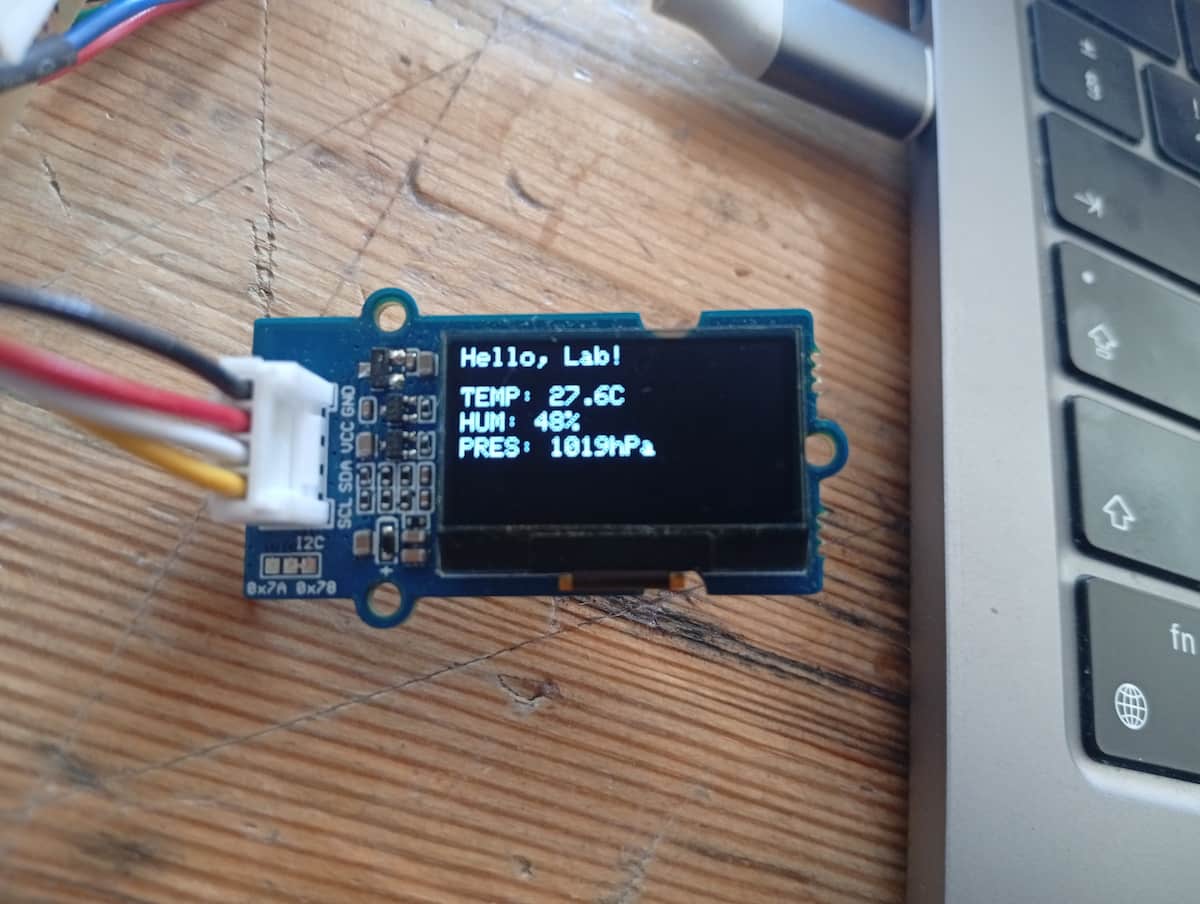
I wrote a little output for the display:
My board used two of the touch pins. (Seems to be hard to press, making them intermittent, so will redesign)
And I printed to the Serial Monitor to make sure:
I am going to try and recreate, but I can’t find my arduino code :(
Note 1: Added through-hole drill holes (and damaged a trace)
It still worked on the continuity test.
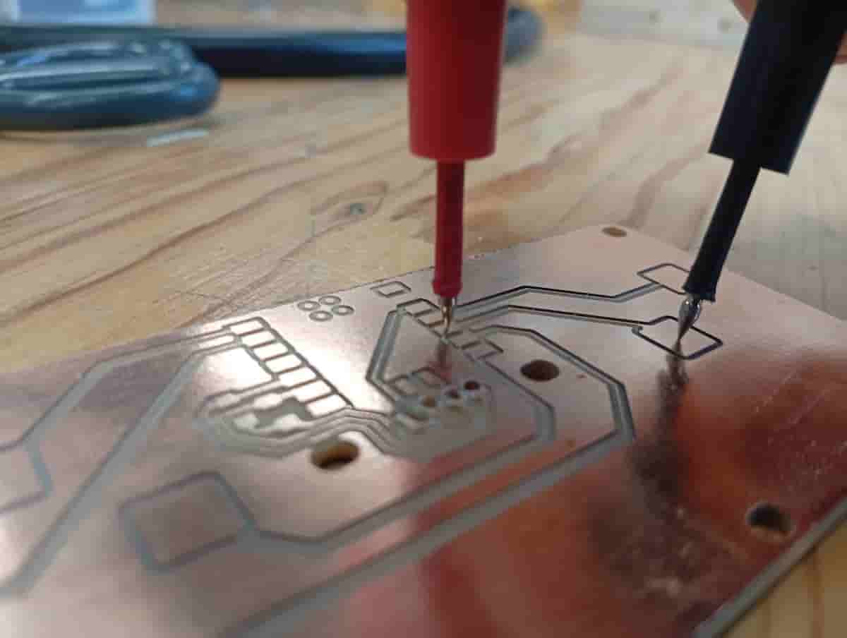
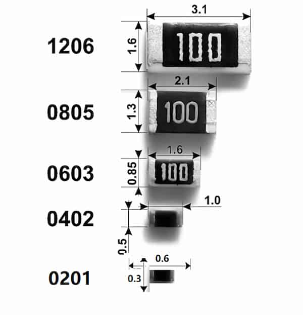
Note 2: Resisters I had were not the right form factor