Assignment Overview
The objective of this week is to transition from digital design to physical fabrication. For Group Assignment, we characterized the specifications of our lab's CNC milling machine, testing various bits and feed rates to determine the optimal tolerances for precise PCB production. For Individual Assignment, I transformed my Week 6 PCB design into a physical board by generating toolpaths, milling the copper-clad substrate, and hand-soldering the SMD components. The process concluded with a functional test to ensure the board was ready for future programming.
Group Assignment:
Learn how to use the CNC in-house
Our instructor showed us how to proceed the CNC machine for copper-clad board production. This is the link of our group work: https://fabacademy.org/2026/labs/chaihuo/docs/week8/week8_group_assignment
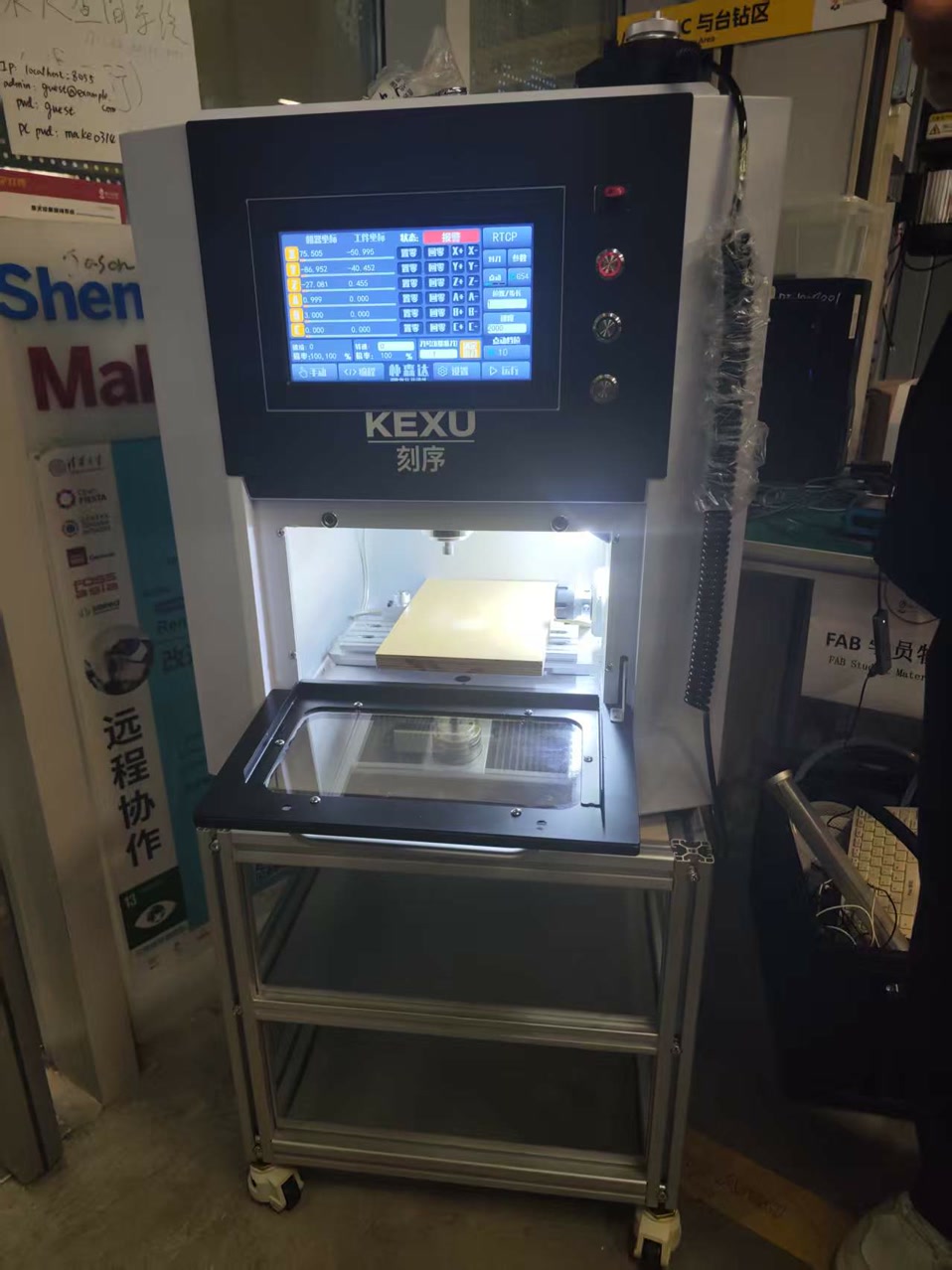
Machine Specifications: KEXU KUXT Precision CNC��
In Chaihuo Makerspace, the milling CNC is KEXU (model: KUXT). At the beginning, I need to know more about the machine. I found the model on the metal label on the back side, and searched it on https://www.kexu.com/.

The KEXU KUXT CNC machine is a professional-grade, high-precision desktop milling system. While primarily used for PCB prototyping in this lab, its robust design allows it to process a wide range of materials including FR4/FR1, Acrylic, Engineering Plastics (POM, Nylon), Machinable Wax, and soft non-ferrous metals like Aluminum and Brass. Its core technical capabilities include:
Spindle Performance: A variable high-speed spindle capable of reaching 24,000 RPM, providing the high surface speed necessary for micro-tooling and clean finishes on both polymers and metals.
Mechanical Precision: Features a positioning accuracy of ±0.01mm and a repeatability of ±0.05mm, driven by high-precision lead screws that ensure intricate details are preserved.
Versatile Motion Control: Supports a maximum feed rate of up to 3,000mm/min, allowing for efficient bulk material removal in 3D milling tasks (such as mold making).
Tooling System: Equipped with a standard ER11 collet, compatible with a wide array of 3.175mm (1/8") shanks, ranging from V-bits for engraving to end mills for structural parts.
Full Enclosure: The system is fully enclosed, which is critical for noise reduction and for containing hazardous dust (like FR4 fiberglass) or coolant spray used during metal milling.
Safety Guidelines
Safety protocols for the CNC machine are designed to handle various material risks:
Enclosure Interlock: The shield must remain closed during operation to protect the user from high-speed spindle contact, flying copper shards, or potential tool breakage.
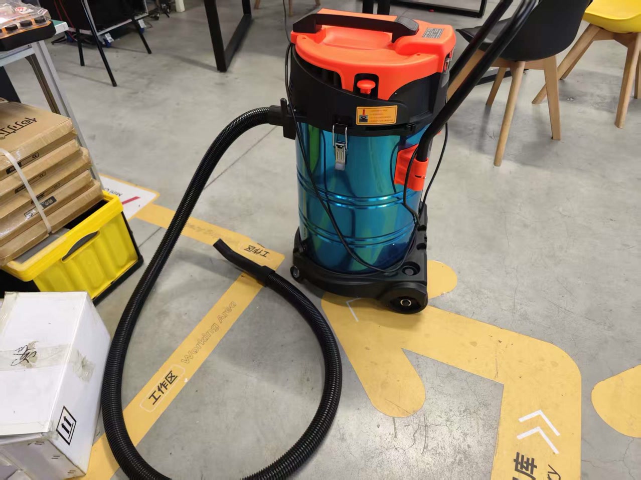
Dust and Debris Management: We utilize integrated vacuum extraction to manage airborne particles. This is especially vital when milling FR4 (fiberglass) or Carbon Fiber, as the dust is hazardous to both lungs and electronics.
Emergency Readiness: I identified and tested the Emergency Stop (E-Stop). This is the primary defense against "crashes" caused by incorrect feed rates or G-code errors.
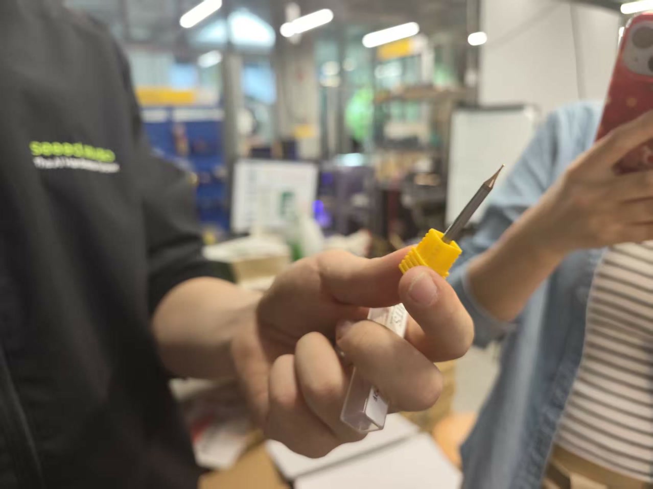
Material Handling: Sharp edges on milled metal and brittle CNC bits require careful handling and the use of appropriate pliers or gloves during setup and cleanup.
Operational Workflow
Our instructor Matthew showed us how to use the machine and do the milling on a copper-clad substrate:
Step 1: Material Mounting
We secured the workboard to the bed. While we used double-sided tape for the copper-clad board, the machine also supports mechanical clamping for thicker materials like aluminum blocks or acrylic sheets.
Step 2: Tooling and Calibration
- We initiated the first phase of the milling process. We installed the appropriate bit for the task (fine bit for traces). The fine bit followed the pre-programmed "route path" to remove the thin top layer of copper, creating the electrical isolation for the traces.
-
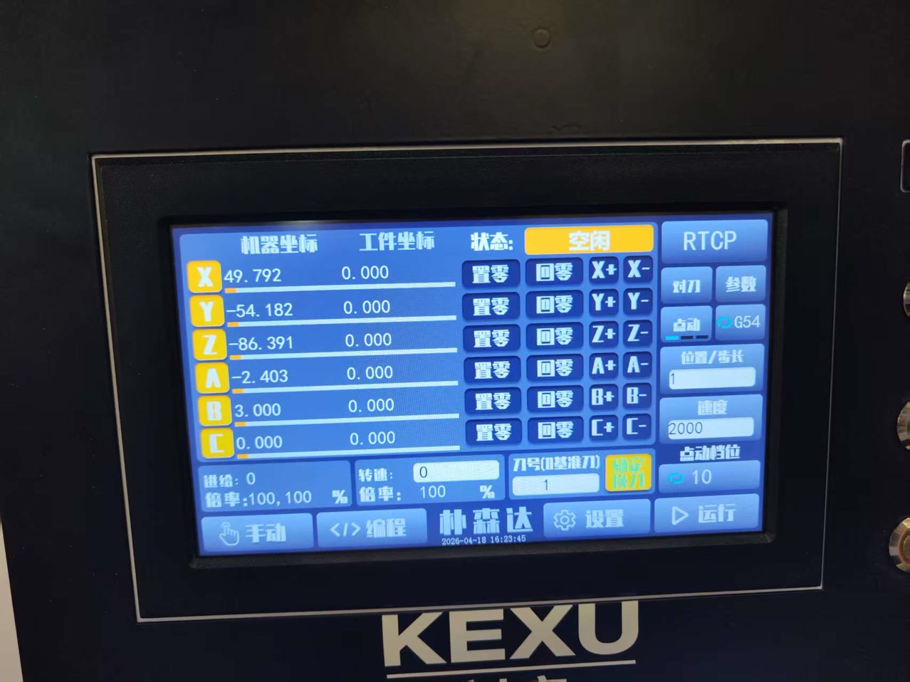
XYZ Zeroing: We moved the spindle to the starting origin via the control interface.
-
Z-Probe: I used the Auto-Tool-Setter (electronic probe). The machine automatically lowered the bit until it touched the probe.
-
We then used the controller's interface to set all axes (X, Y, Z) to zero simultaneously, establishing the master origin for the job.

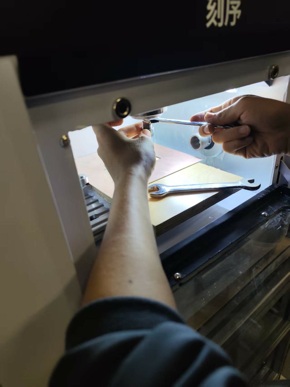
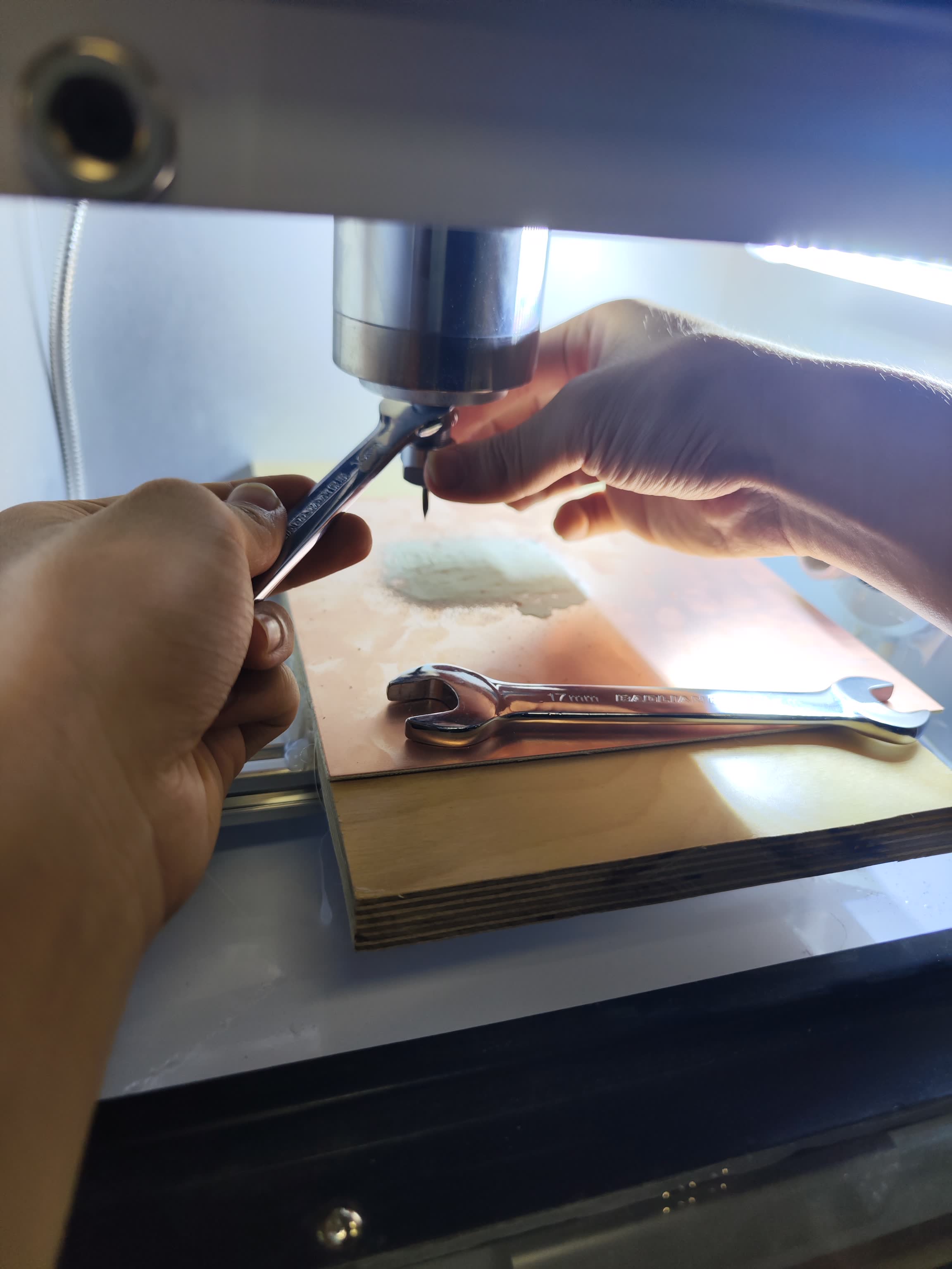
Once the routing was complete, we used the wrench again to swap the fine bit for a thicker end mill.
We re-verified the Z-axis zero point with the new bit to account for any difference in tool length.
We executed the final "cut through" command. The thicker bit milled along the Edge.Cuts path, cutting entirely through the PCB substrate to separate the finished board from the stock material.
After the spindle stopped and the enclosure was opened, we used a vacuum to remove the copper and fiberglass dust. Then carefully removed the finished PCB from the bed using a spatula.
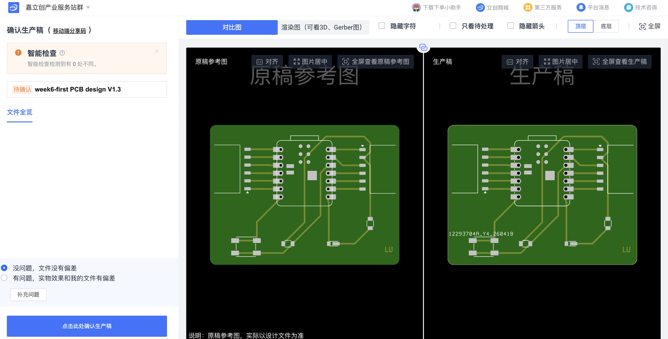
Send PCB Design to board factory for production
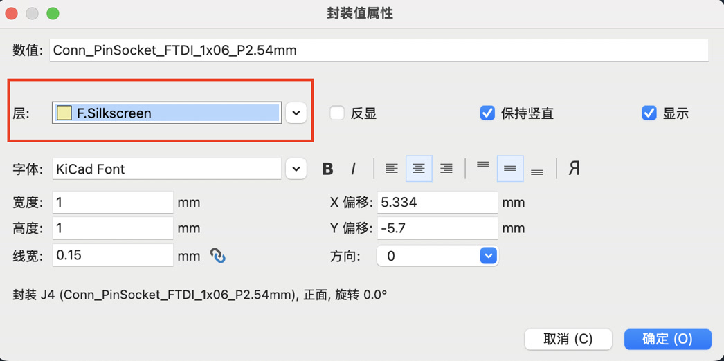
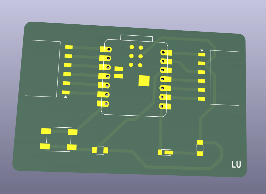
I identified text exceeding the board boundary. Although I don't need these texts to be produced, I would like to figure out how to make the silk screen texts first. I first went to the Appearance Manager on the right side of the screen and clicked on the F.SilkS (Front Silkscreen) layer to make it active.
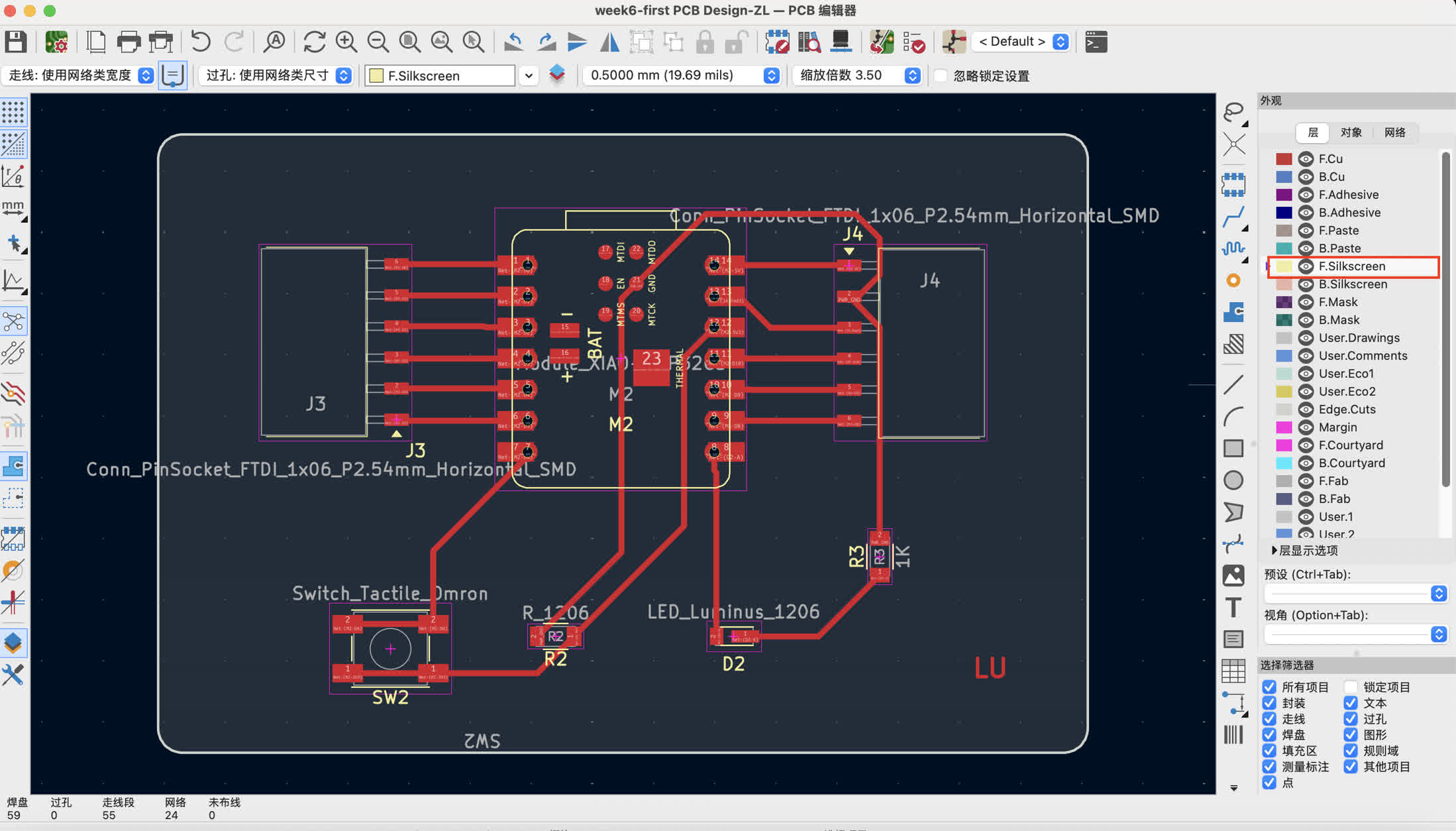
I corrected it by selecting the text, and move it within the Edge.Cuts, and shorten the texts which are too long. For component texts assigned to the wrong layer, I double-clicked the text to open Footprint Properties and changed the Layer from F.Fab to F.SilkS.
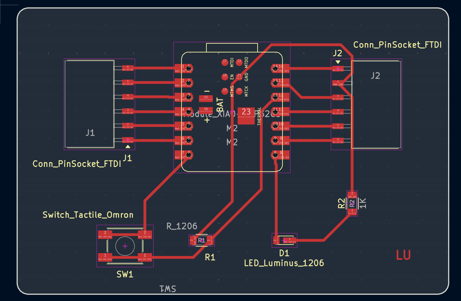
This is the work after fixing the texts in F.Silkscreen.
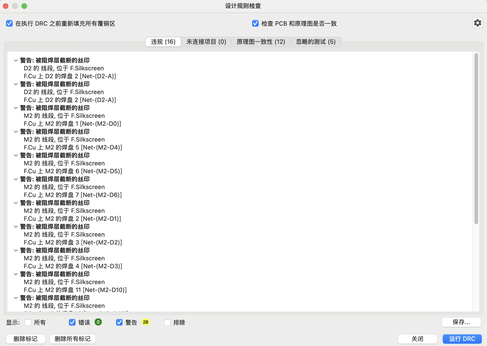
I ran DRC again to see if any errors, there's 0 error.
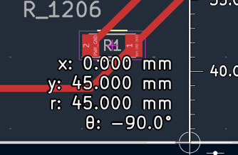
To ensure correct machine alignment at the board factory, I set a manual coordinate origin. I navigated to the top menu bar Place > Drill/Place File Origin.
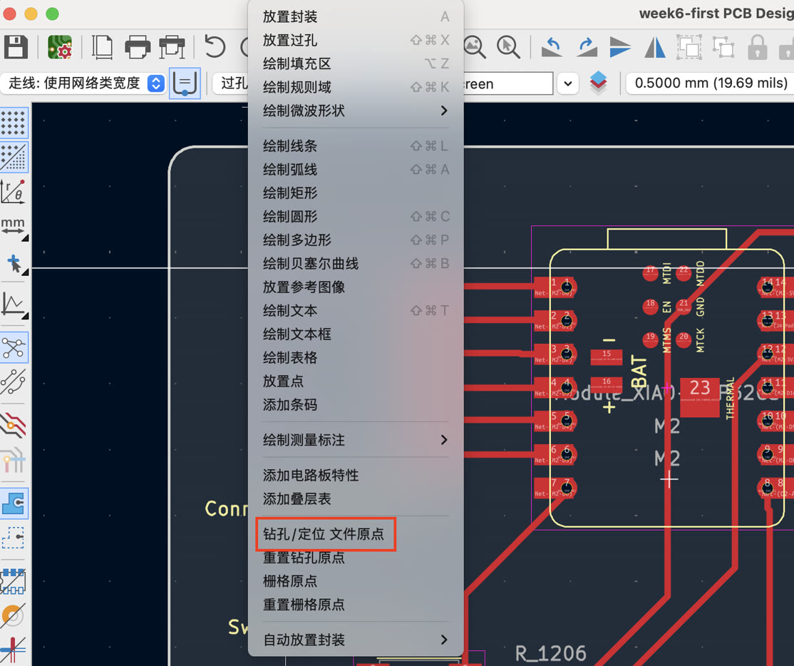
My cursor changed to a crosshair; I then moved it to the vertex of the Edge.Cuts frame and clicked exactly on the bottom-left corner to anchor the $(0,0)$ reference point.

I went to File > Fabrication Outputs > Gerbers (.gbr). In the Plot window, I checked the boxes for the following layers: F.Cu, F.SilkS, F.Mask, and Edge.Cuts. I ensured the "Use drill/place file origin" checkbox was selected so the export would use my custom $(0,0)$ point. I then clicked the Plot button to generate the files.
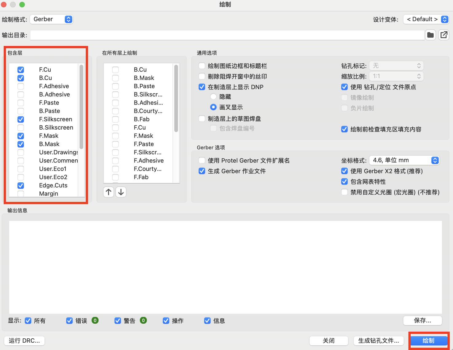
Then I have the Gerber files as below to send them to design house.
The complete Gerber package is here: gerber.zip
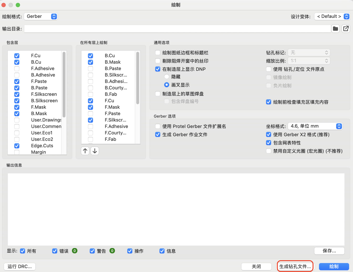
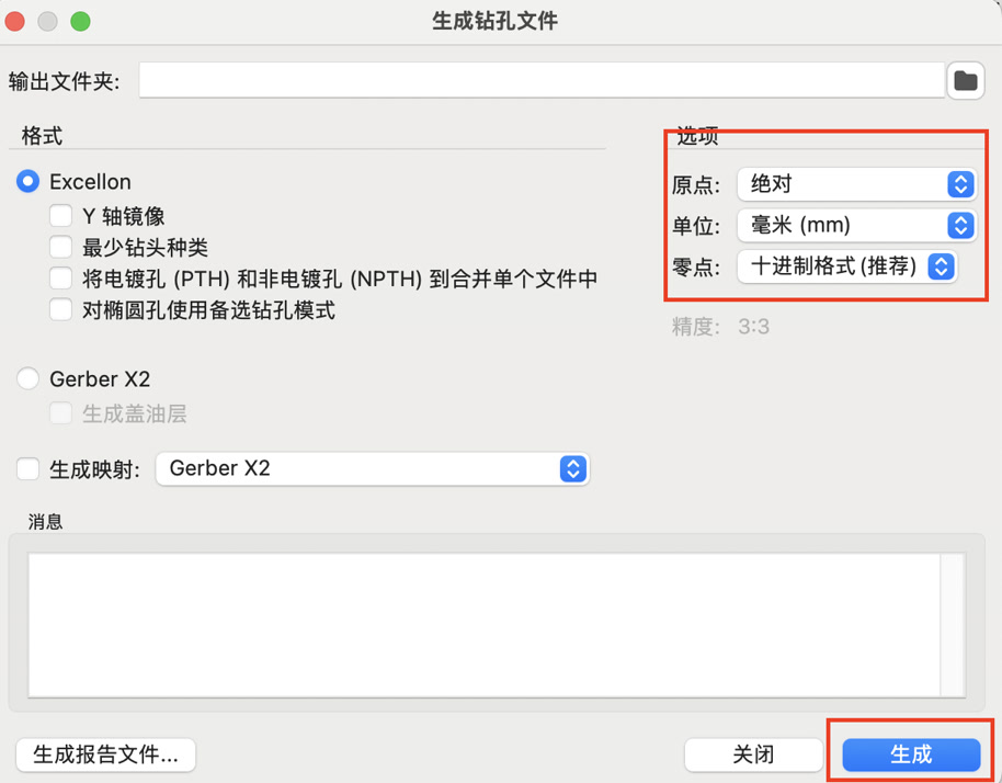
[week6-first PCB Design-ZL-Edge_Cuts.gbr] [week6-first PCB Design-ZL-B_Mask.gbr] [week6-first PCB Design-ZL-F_Mask.gbr] [week6-first PCB Design-ZL-F_Silkscreen.gbr] [week6-first PCB Design-ZL-B_Cu.gbr] [week6-first PCB Design-ZL-F_Cu.gbr]While the Gerber dialog was still open, I clicked the Generate Drill Files... button located in the bottom-right corner. In the settings, I selected Millimeters for Drill Units and Decimal format for Zeros Format. I clicked the Generate Drill File button to produce the .drl file containing the coordinates for the through-hole pin sockets.
Understanding Gerber Layers for Manufacturing
To ensure a successful production at JLCPCB, I generated a set of independent Gerber files as above. At the beginning I did not quite understand the meaning of each gerber and why there are several gerbers. I checked on Google Gemini and realized each file corresponds to a specific physical layer or process:
Copper Layers (The Circuitry)
--F.Cu (Front Copper): Contains the top-layer electrical traces and pads.
--B.Cu (Bottom Copper): Contains the back-layer traces. Even for single-sided designs, factories prefer this file to define the bottom pads.
Solder Mask Layers (The Protection)
--F.Mask / B.Mask: These files define where the Solder Mask (the green coating) should NOT be applied. The areas defined here will expose the bare copper for soldering.
Silkscreen Layers (The Labels)
--F.SilkS (Front Silkscreen): The white ink layer used for component outlines, logos, serial numbers and reference designators.
--B.SilkS (Bottom Silkscreen): Information printed on the back. Since I have no components on the back, this is optional.
Mechanical and Drill Layers (The Shape)
--Edge.Cuts: This defines the physical boundary and shape of the PCB. The factory uses this to CNC-mill the 2mm rounded corners of my board.
--Excellon Drill File (.drl): Technically not a Gerber but a CNC instruction file that tells the machine where to drill holes for the through-hole pin sockets.
Technical Layers (Auxiliary)
--F.Paste / B.Paste: Used for creating stencils for solder paste in automated SMT assembly. Since I am hand-soldering, these are not required.
--F.Fab / B.Fab: Documentation layers for assembly instructions. These are for human reference and are not required for fabrication.
For this assignment, I bundled the following files into my final ZIP package to ensure a complete and error-free fabrication:
- F.Cu & B.Cu (Circuit paths)
- F.Mask & B.Mask (Insulation and soldering access)
- F.SilkS (Component identification)
- Edge.Cuts (Physical board shape)
- Drill File (.drl) (Hole locations)
I chose JLCPCB as my design house because it provides an industry-standard fabrication service that offers high-precision manufacturing, and delivers the PCB within 48 hours. Website: https://www.jlc.com/?from=PZ-pLpu&s=JC

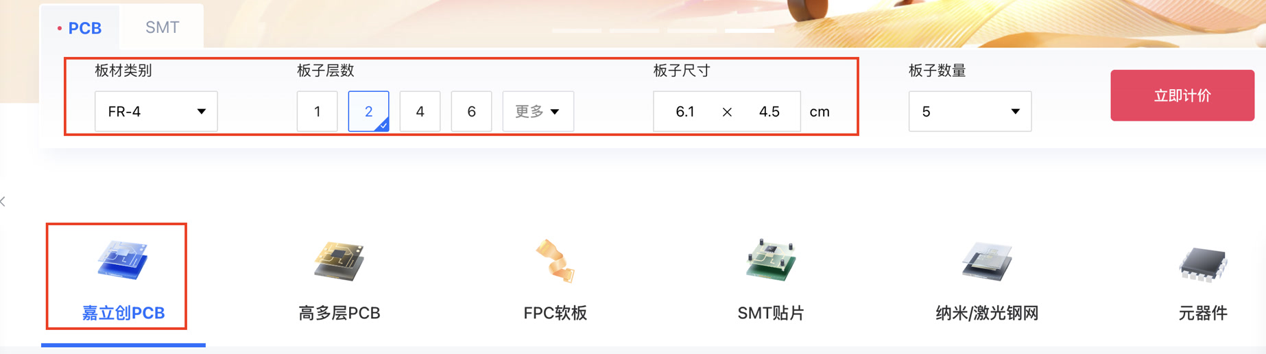
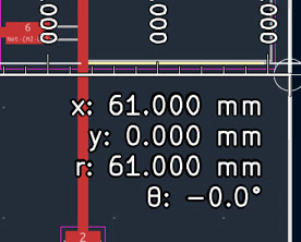
Since the system requires dimensions during the initial form-filling stage, I returned to KiCad to verify the board's footprint. I activated the Measure Tool and clicked the opposite corners of my Edge.Cuts layer. I recorded the exact width of 61 and height of 45 in millimeters and entered these values into the JLCPCB order form to ensure the quote and manufacturing scale were accurate.
Before uploading any files, I accessed the JLCPCB ordering interface to manually configure the production specifications. This required me to understand the engineering implications of each setting. Some key parameters as below:
Base Material & Thickness: I selected FR-4 with a 1.6mm thickness. FR-4 provides the necessary mechanical rigidity for the XIAO ESP32C3, and 1.6mm is the industry standard that ensures durability.
Solder Mask & Silkscreen: I chose a Green solder mask, it's general and JLC can deliver it faster.
Surface Finish (Leaded HASL): I specifically chose Leaded HASL because the lead content lowers the solder melting point. This is a critical decision to facilitate easier manual SMD soldering, ensuring smoother joints during assembly.
Copper Weight: I set this to 1oz, which is perfectly calculated to support the current requirements of my track width without voltage drops.

After confirming the parameters and submitting the initial order form, I reached the file submission stage. I located the ZIP archive containing my Gerber and Excellon drill files. I dragged and dropped the package into the upload zone, where the system then cross-referenced my uploaded design against the parameters I had just configured.

I paid the order of RMB 43, checked the files for production on JLC platform and confirm it.
Waiting for production and PCB delivery.
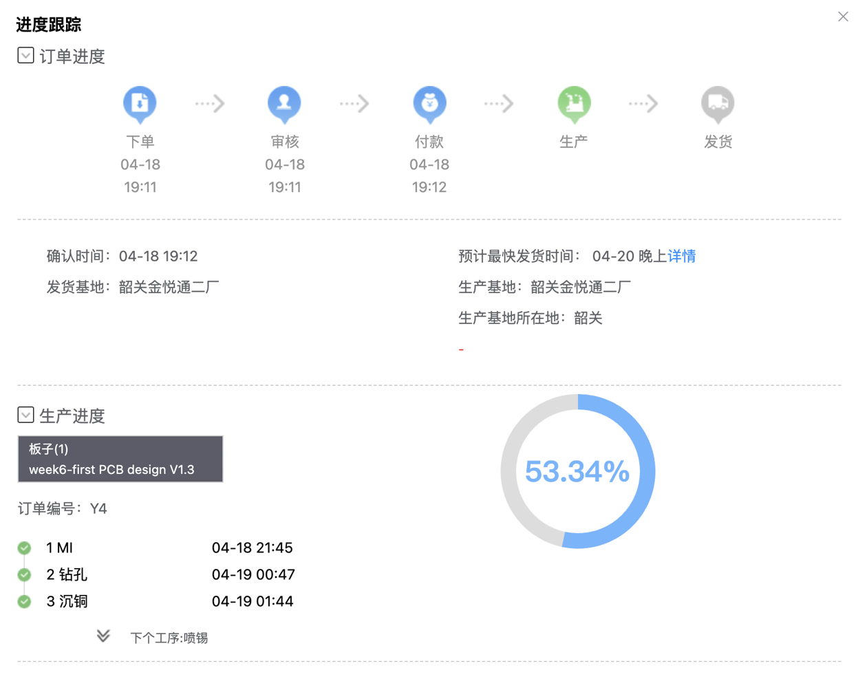
Finally I received my boards within 48 hours,
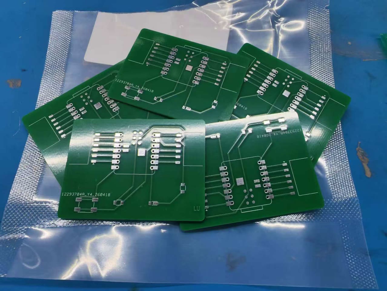
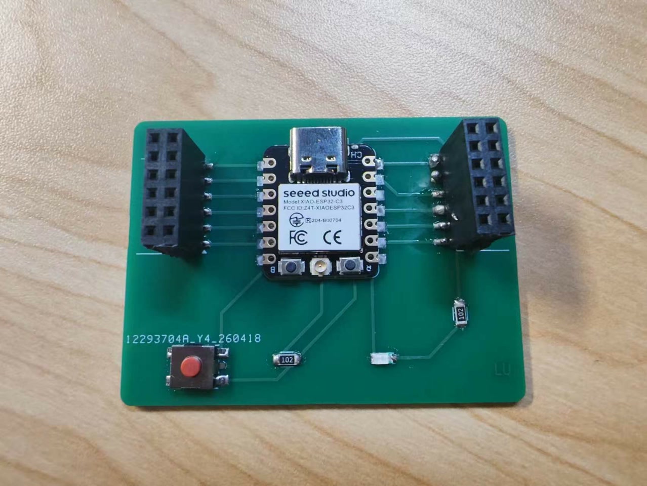
I soldered XIAO ESP32C3 and other components to the PCB:
Individual Assignment: Production in-house
Generate G-code

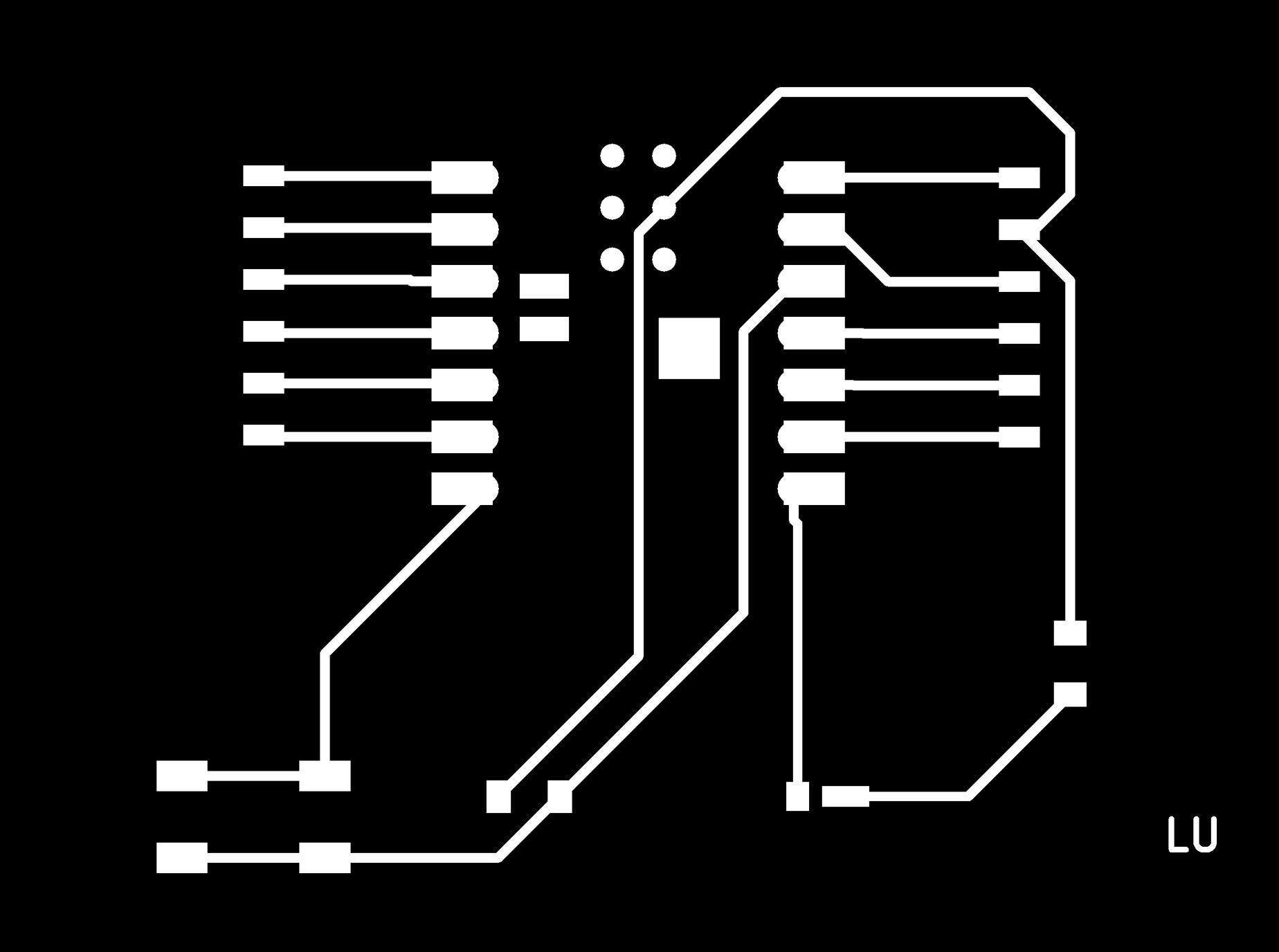
I started by exporting the necessary layers from KiCad. I generated two primary files,
--F.Cu (Front Copper): For the circuit traces and pads.
--Edge.Cuts: For the physical board perimeter and shape.
The exported Gerber package is here: gerber.zip
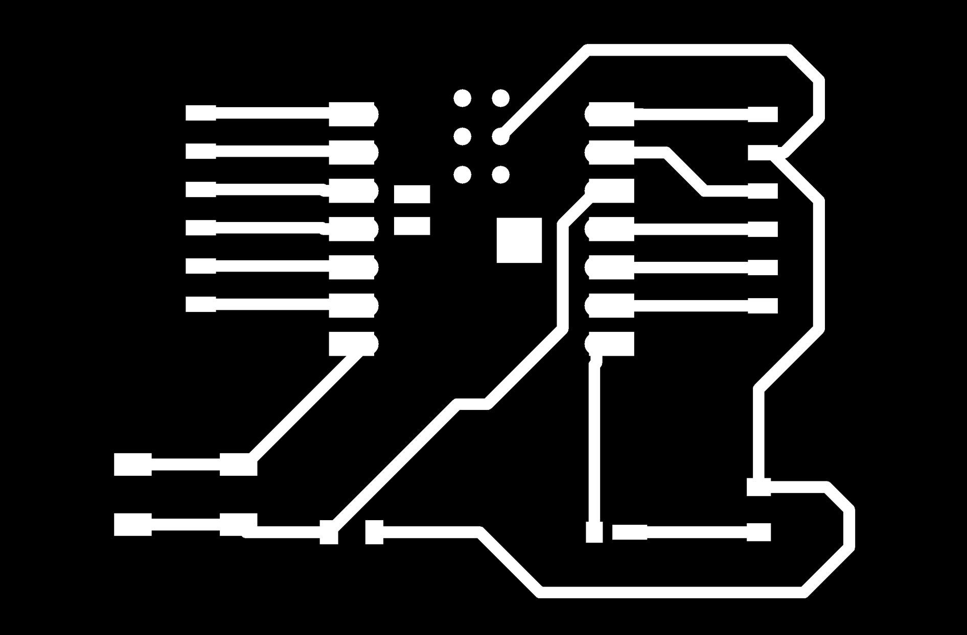
[week6-first PCB Design-ZL-Edge_Cuts.gbr] [week6-first PCB Design-ZL-F_Cu.gbr] Step 2: Converting Gerber to PNGSince the toolpath generator I used (Mods CE) works best with high-resolution raster images, I converted my vector Gerber files into PNG format. I used the online tool Gerber2PNG by Fablab Kerala
I uploaded my Gerber files F.Cu and Edge.Cuts to the converter, and click the red button "Generate PNG" on the left side. Then I saw png files on the right.
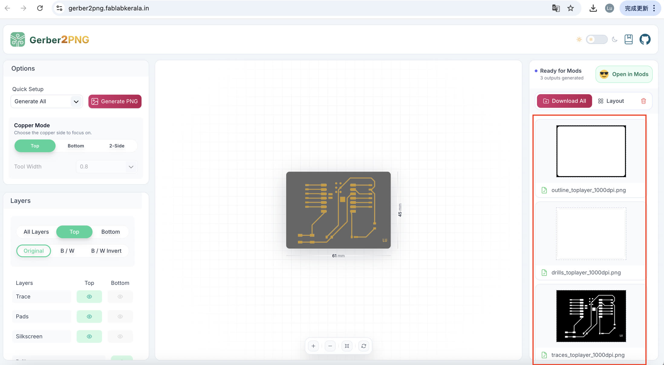
Then I downloaded two files: traces.png (representing the circuit) and outline.png (representing the board boundary). This tool ensures the DPI and scale remain consistent between the two files, which is critical for alignment.

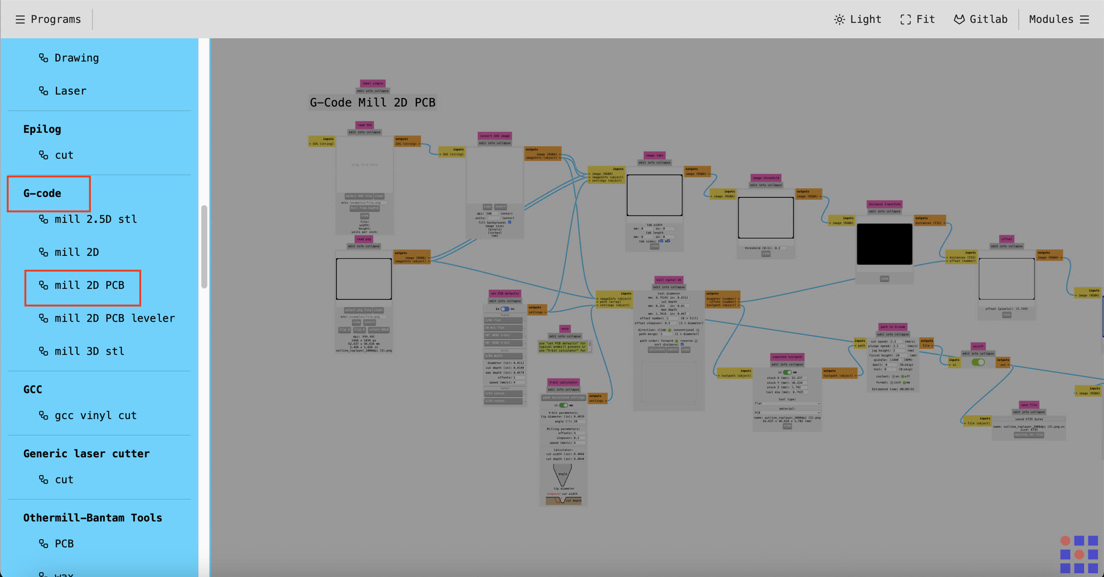
I used the Mods Project (Mods CE) to calculate the toolpaths and export the G-code. First, I navigated to programs->machines->G-code_>mill 2D PCB.
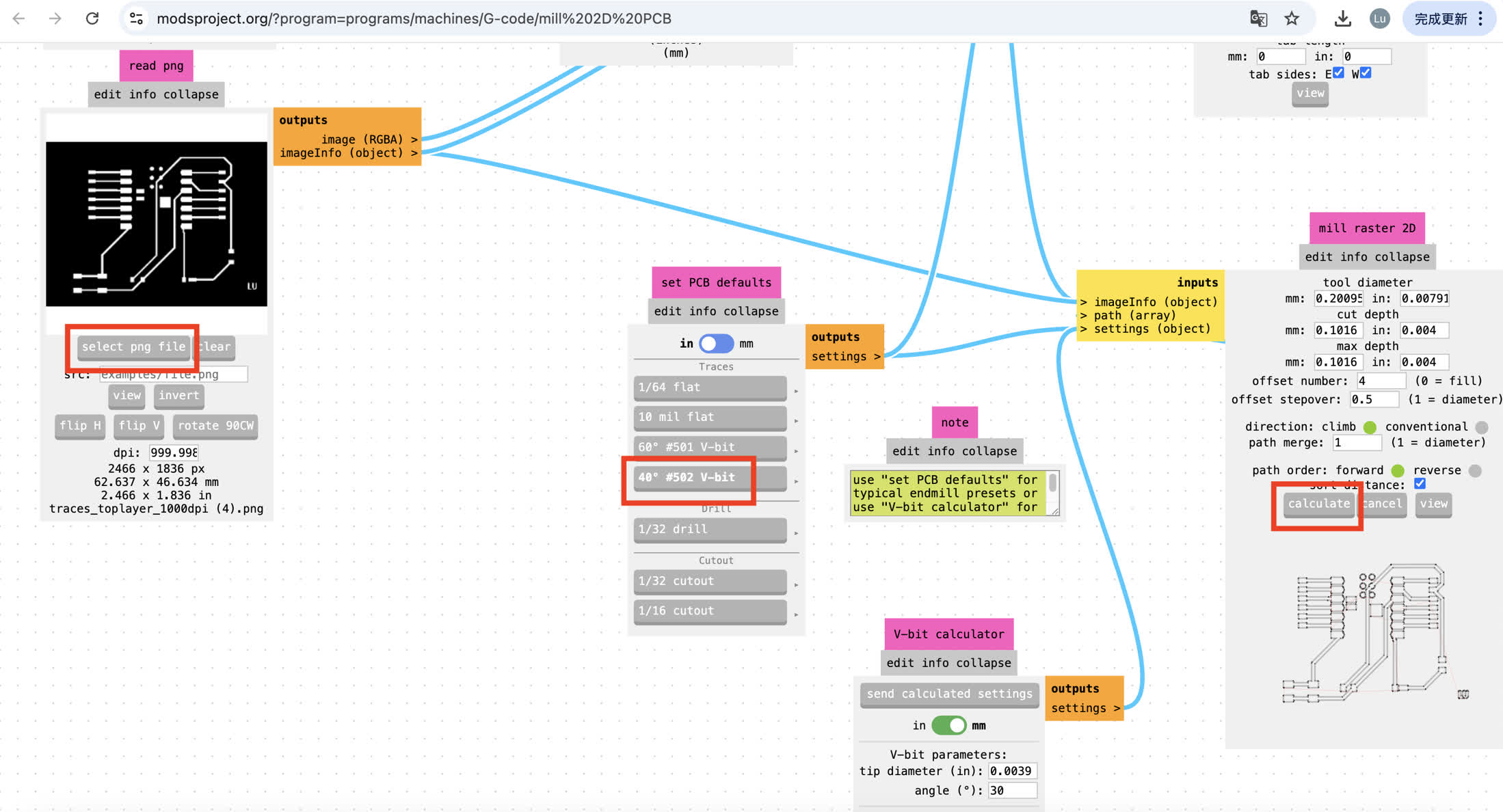
- Generate the g-code for traces:
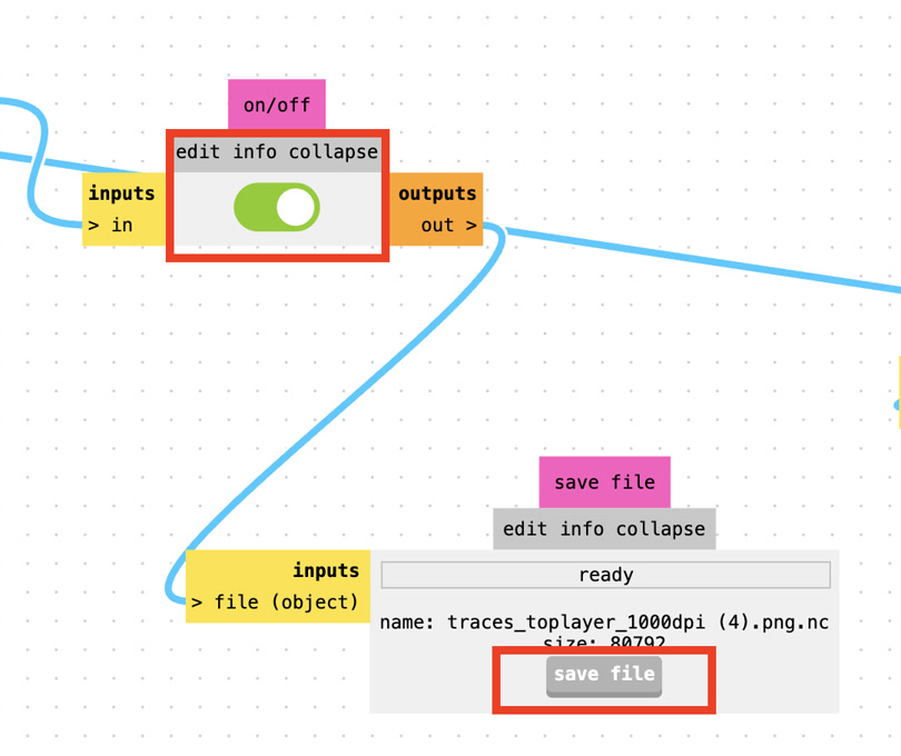
I imported the png file of traces into the read png module. In the PCB defaults module, I selected 40° #502 V-bit. I turned on the button of "edit into collapse". I clicked calculate to generate the toolpath and saved the resulting .nc file.
- Generate the g-code for outline:
It's almost the same settings as what I did for the file of traces, just adust the setting in PCB defaults module, I selected 1/32 Drill.
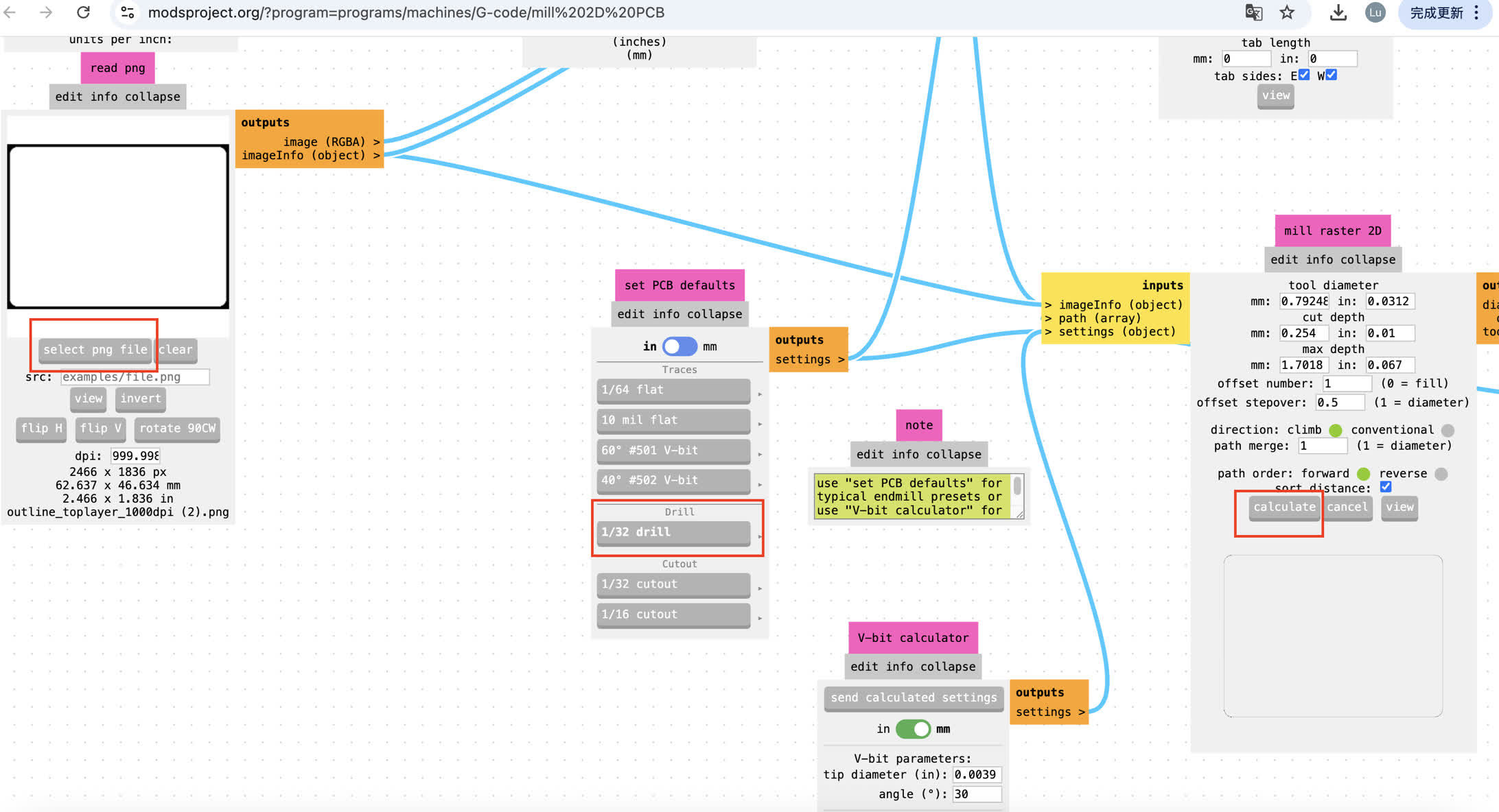
At the end of this workflow, I had two .nc (G-code) files ready for the CNC machine:
traces.nc: For isolation routing of the copper paths using the fine bit.
outline.nc: For cutting through the entire PCB substrate using the thick bit.
However, the original G-code file could not run well on the machine, when it started to operate, it showed error. Thus I asked ChatGPT to check it and it gave me these steps to update my G-code. The reason is that, the original trace file is more minimal compared to the functional one. The operational file contains additional commands such as tool selection, tool length compensation (G43 H1), coolant activation (M08), a program identifier, and a startup sequence that is better suited for the machine controller.
Cutting peration of milling on copper-clad board
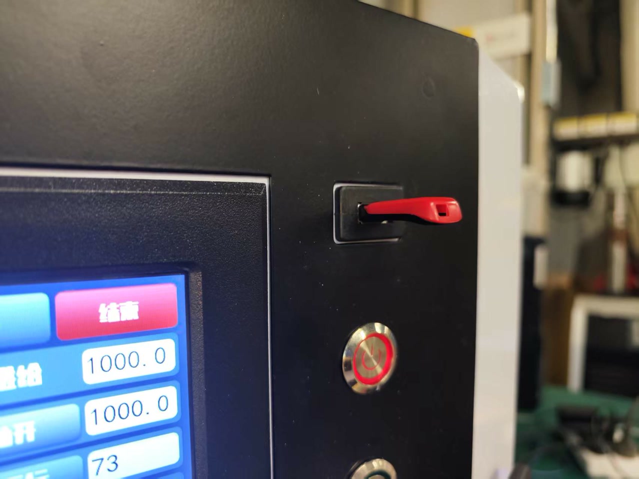
I copied the updated G-code file to the hard drive, and inserted it to the CNC machine.
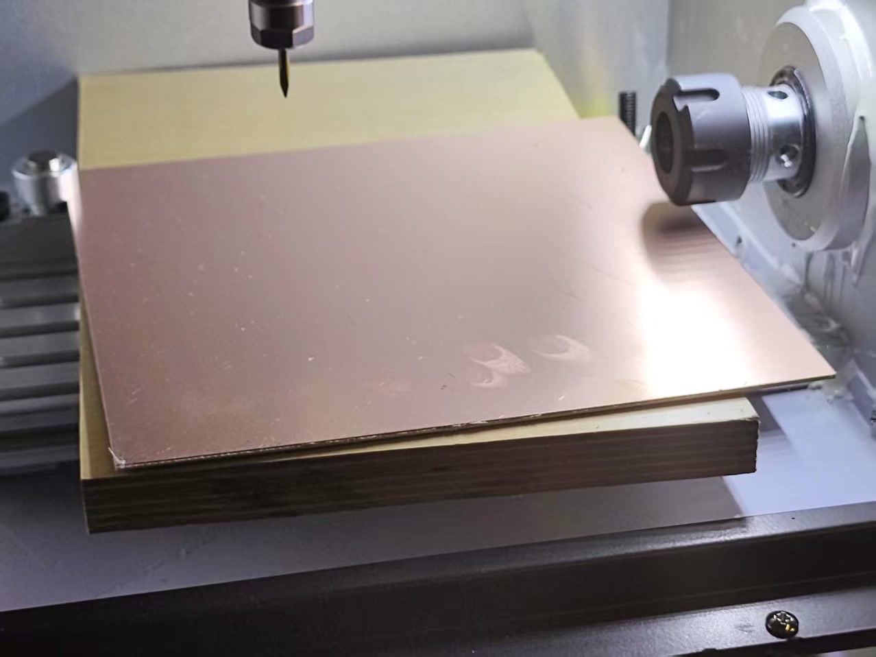
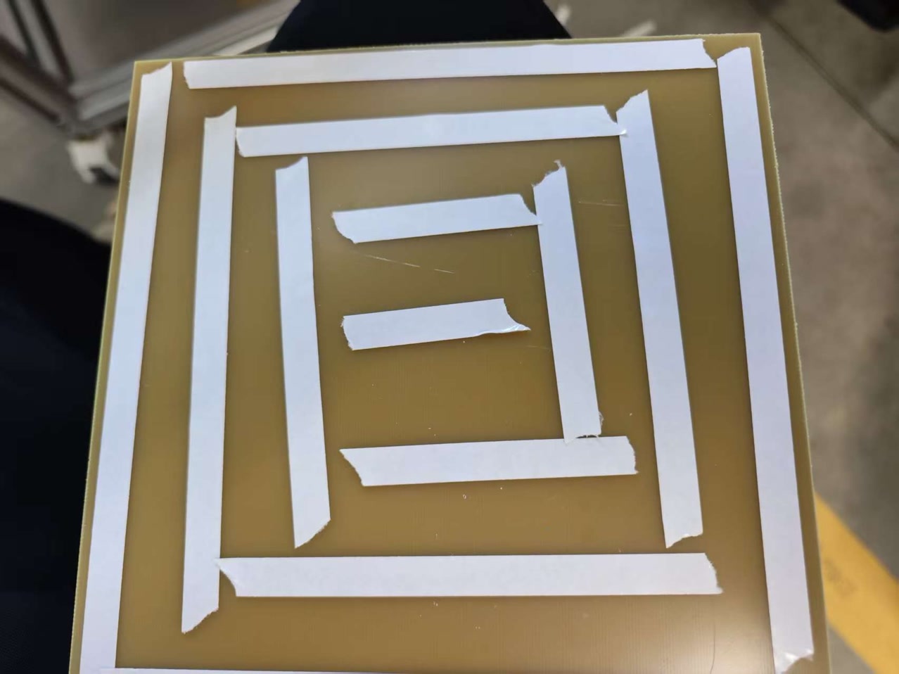
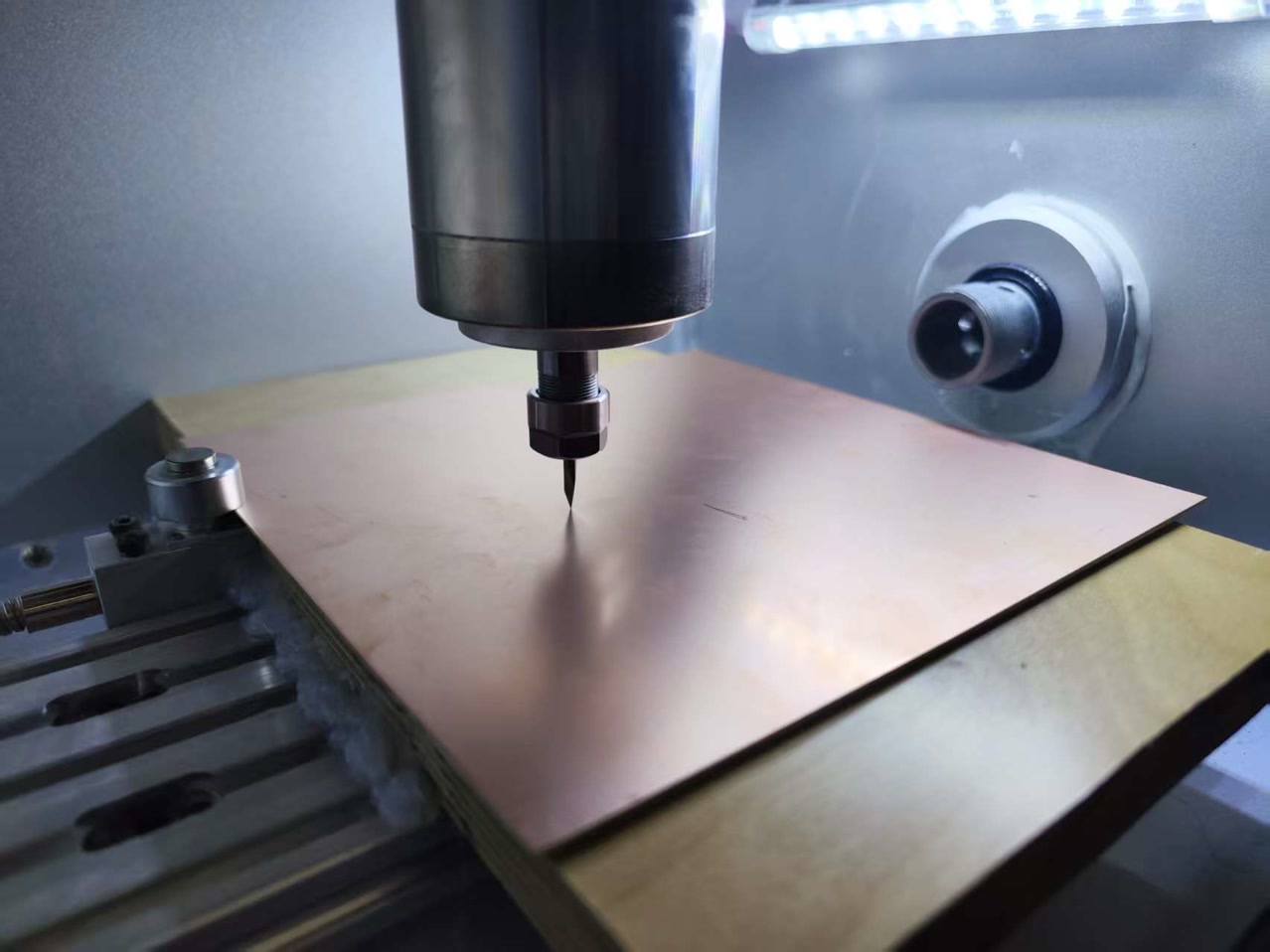
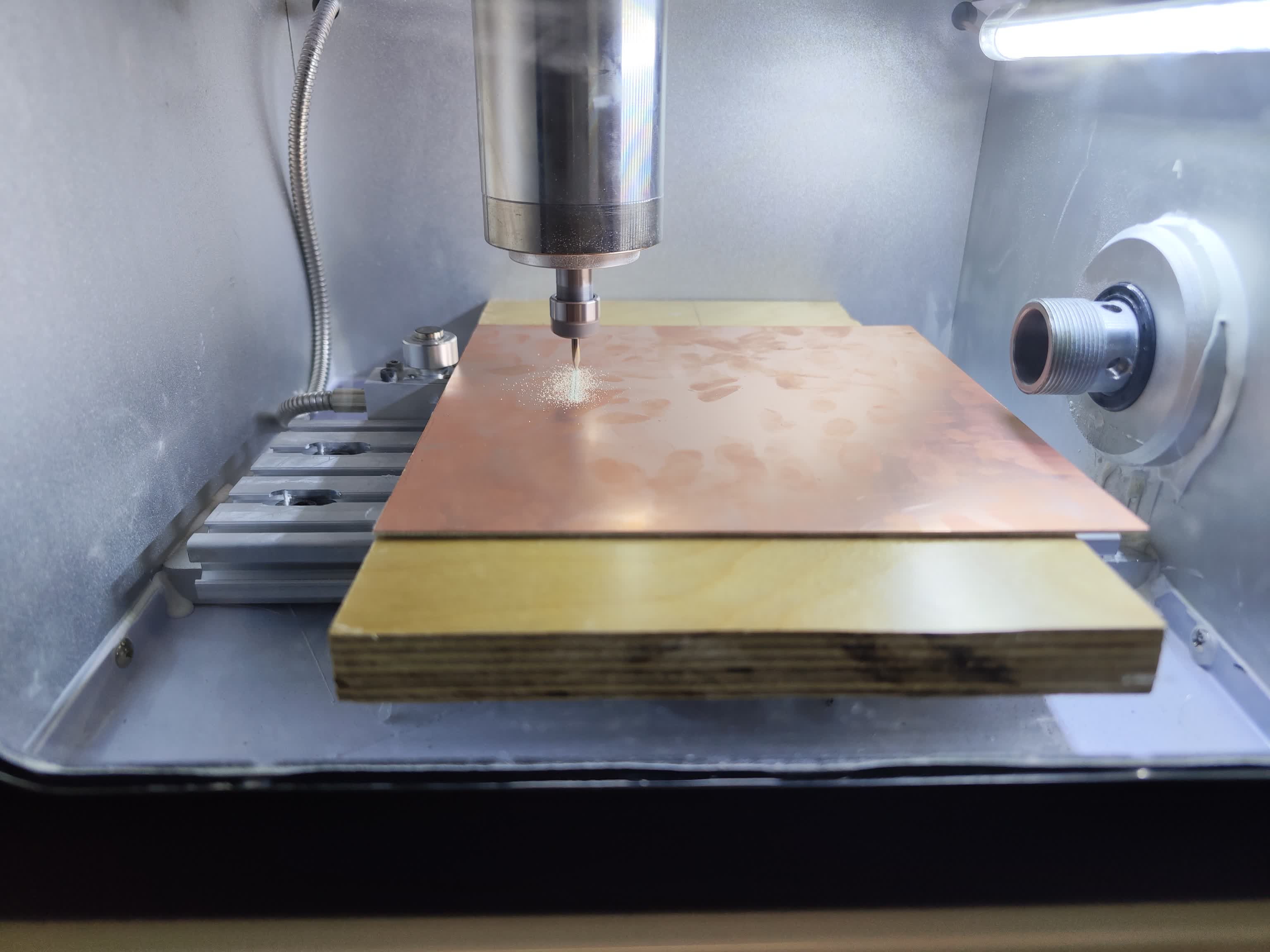
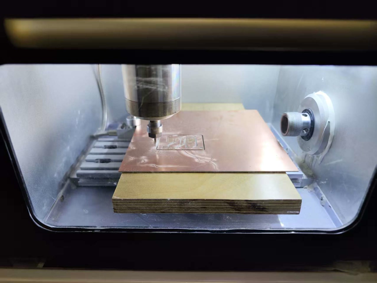
I prepared a piece of copper-clad FR4 board. I applied high-strength double-sided tape to the backside of the board, covering as much surface area as possible to prevent any vibration or "bowing" during milling. I then pressed the board firmly onto the machine's flatbed, ensuring it was parallel to the X-axis.
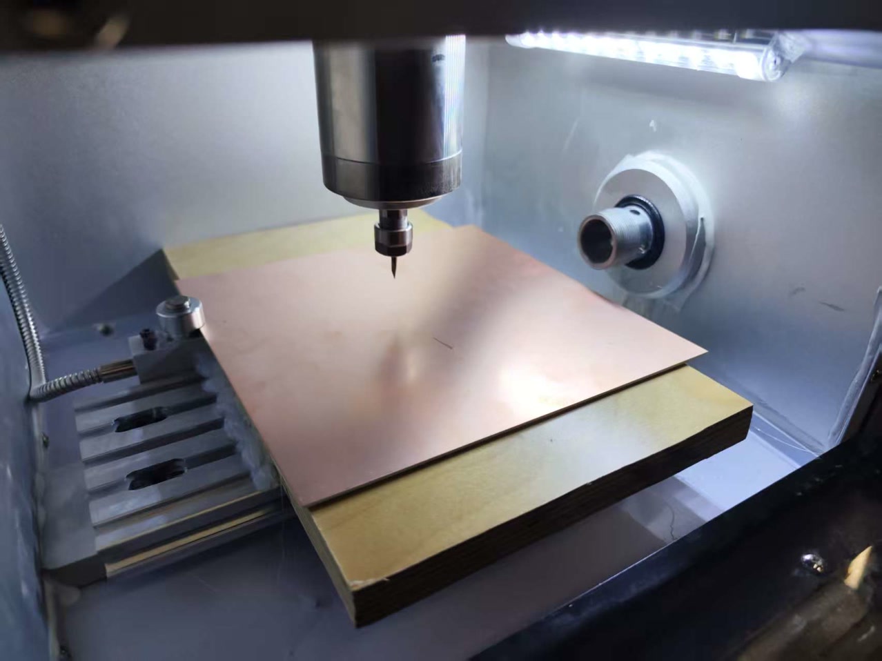
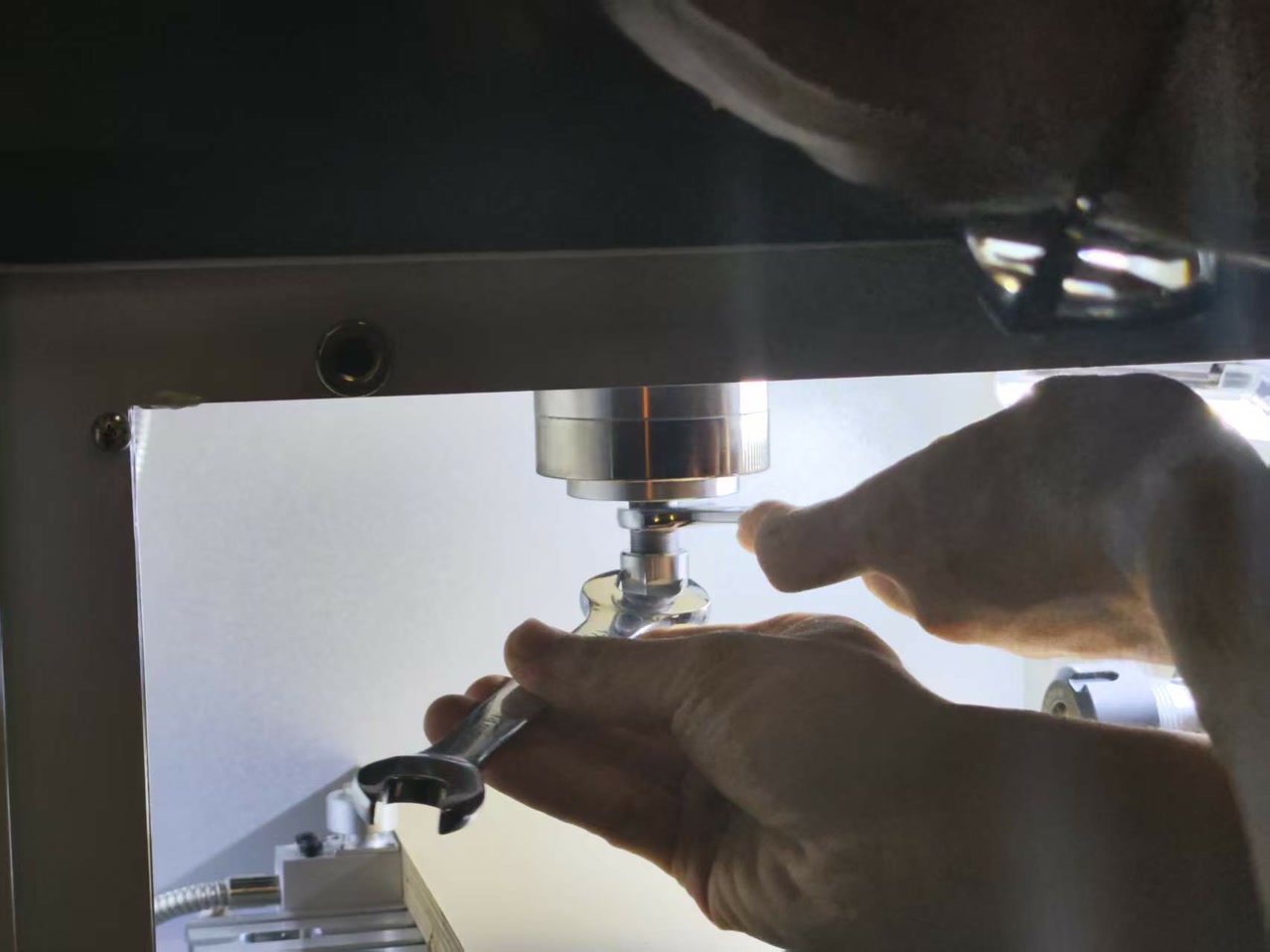
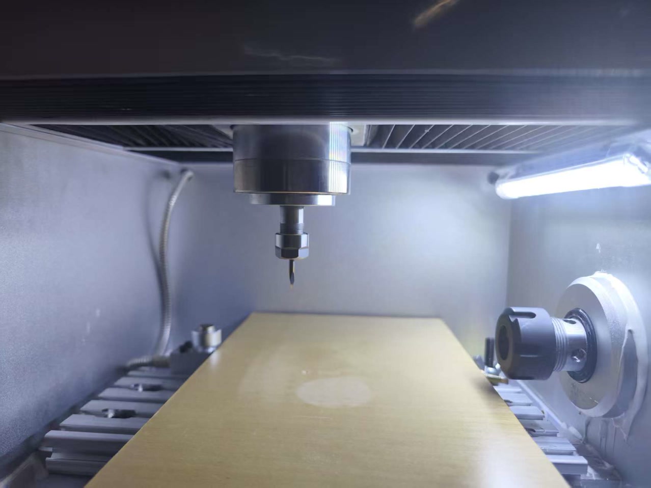
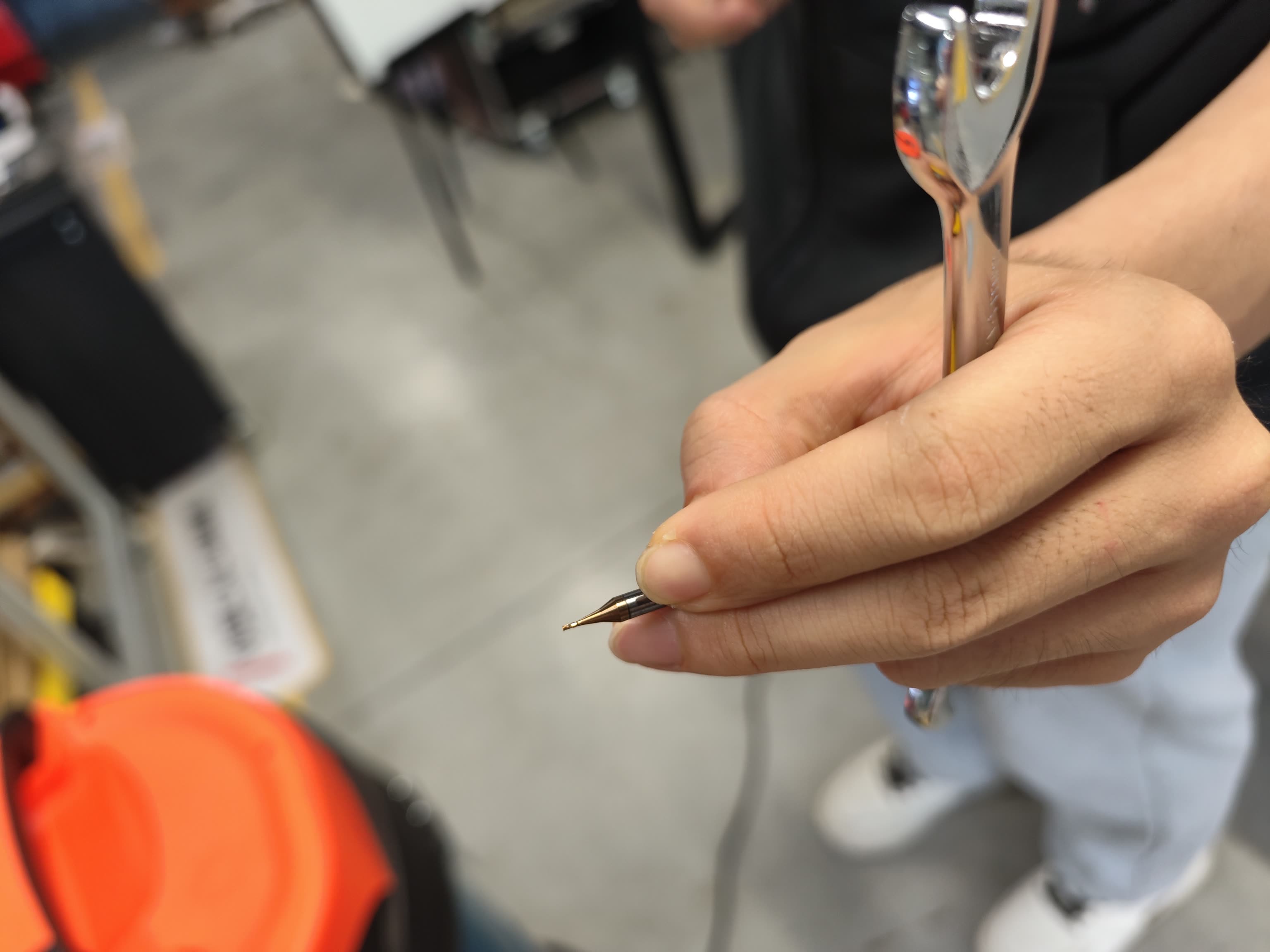
To begin the first phase of milling, I used 2 wrenches to manually loosen the collet and installed a fine engraving bit (V-bit) for the isolation routing.
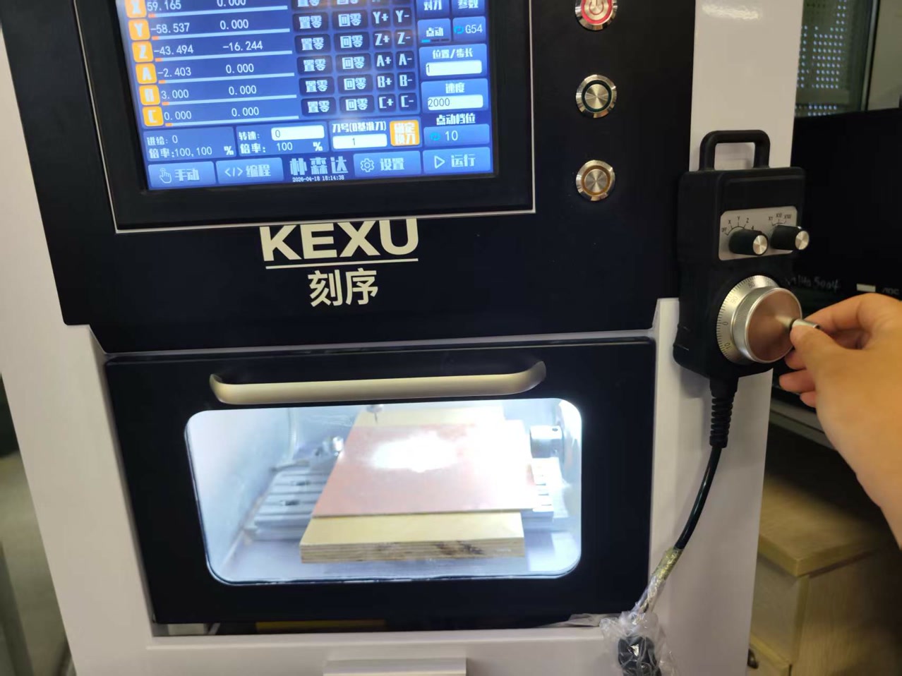
Once the tool was secured, I used the handheld remote controller to jog the spindle to the desired starting position on the bottom-left corner of my potential copper-clad board.
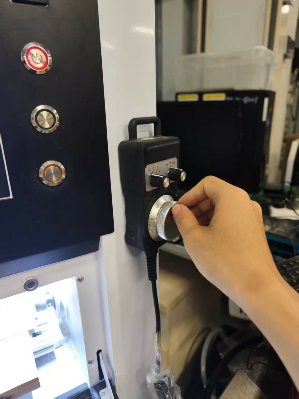
I carefully lowered the Z-axis until the tip of the bit was just barely touching the copper surface.
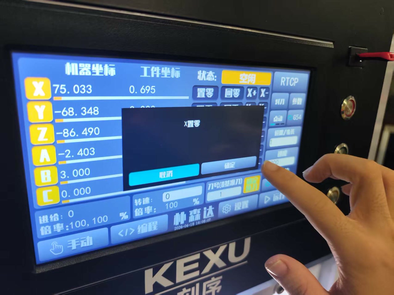
At this precise point, I used the controller’s interface to execute the "Set All Zero" command, effectively anchoring the X, Yand Z coordinates at (0,0,0) as the master origin for the entire project.
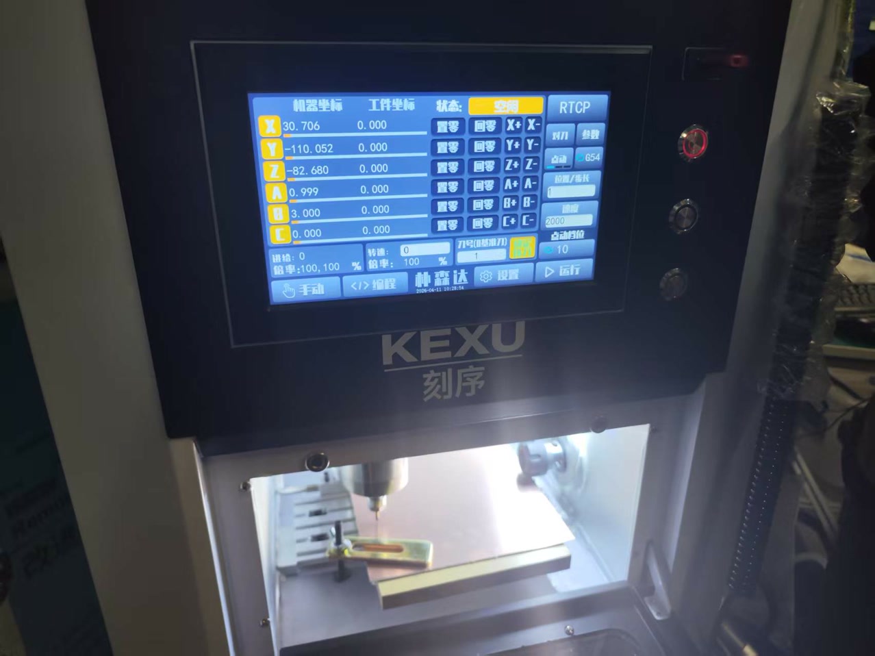
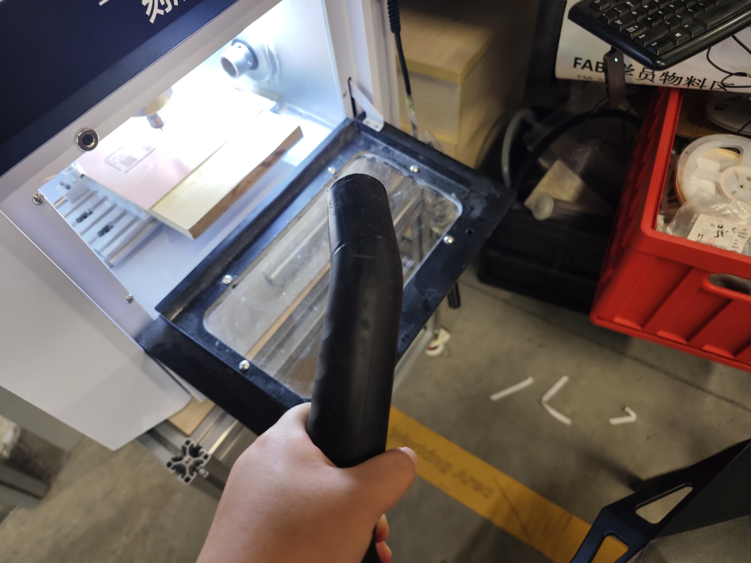
Now it's time to cut the traces. I closed the door of the cutting area.
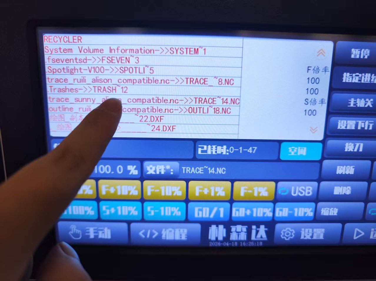
I pressed “Manual" on the left bottom, to go to the menu. I chose "document" to locate my file which runs on the machine for cutting work.

I found my file and clicked it.
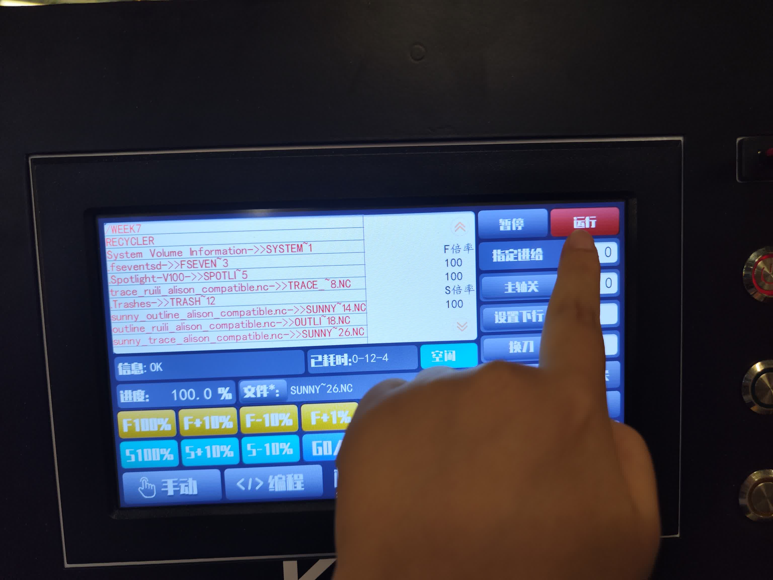
Then I press the “RUN" red button on the top right, to run the cutting of the traces.
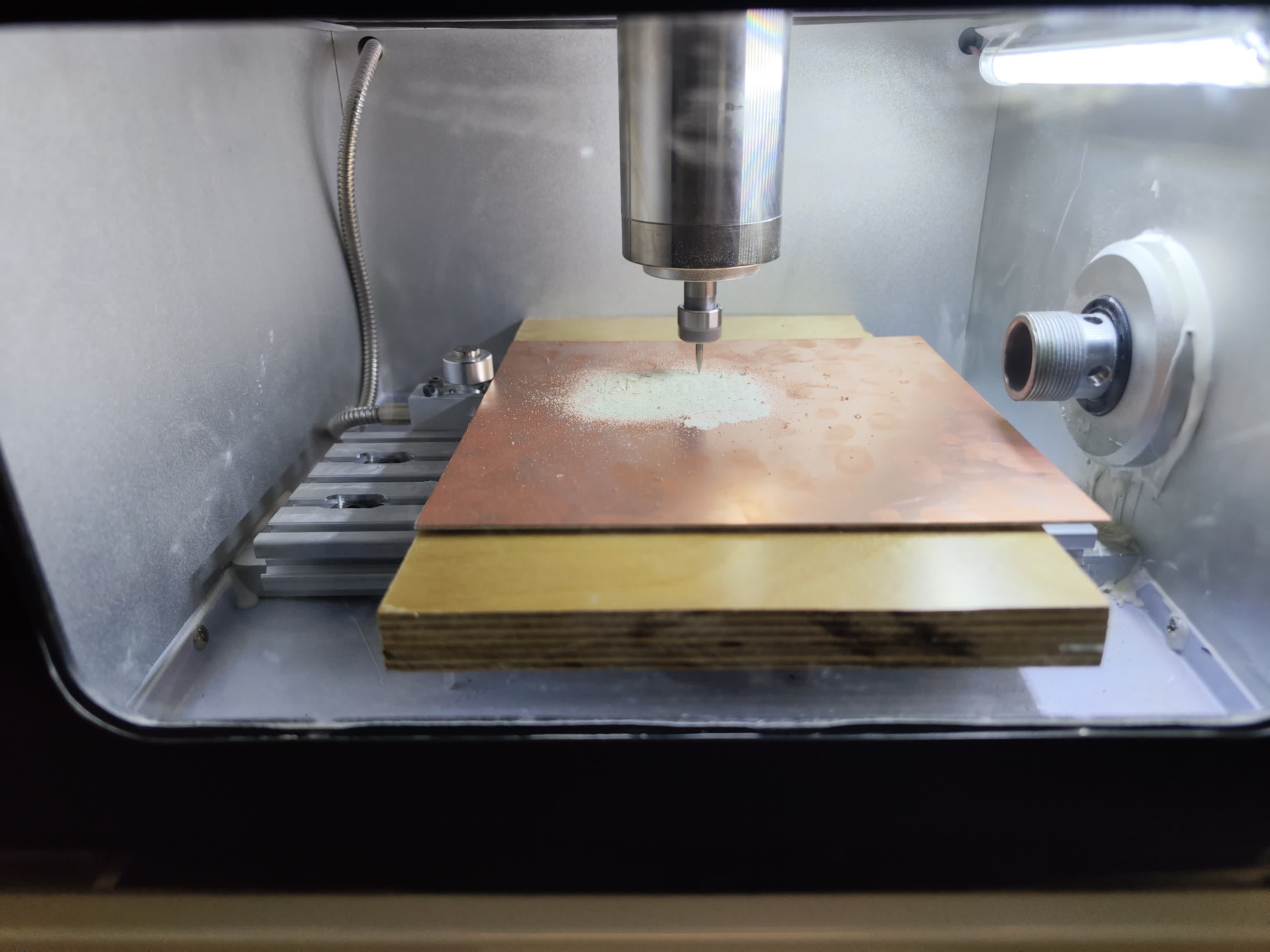
The machine started to cut, I waited for the traces to be born. The machine followed the "route path" generated in Mods CE, removing the top layer of copper to create the necessary electrical isolation for my circuit traces. During this stage, I stayed near the machine to monitor the cut depth, ensuring that the V-bit was clearing the copper without excessively damaging the underlying fiberglass substrate.
After the traces were successfully milled, the spindle returned to the home position. I then performed a tool change to prepare for the board edge cut. Using the wrench again, I swapped the fine bit for a thicker end mill.
Since the new bit had a different physical length, I had to recalibrate the Z-axis only by bringing the tip down to the copper surface again; however, I kept the original X and Y zero points to ensure the board outline would align perfectly with the existing traces. I then loaded the outline file and started the final cycle, where the machine performed multiple passes to cut entirely through copper-clad board.
The manual operation is quite similar to cutting traces. After all the settings for outline on machine, I pressed "RUN" again to draw the board edge.
Once the spindle came to a complete stop, I opened the enclosure and used a vacuum to thoroughly remove all copper shards and hazardous fiberglass dust.
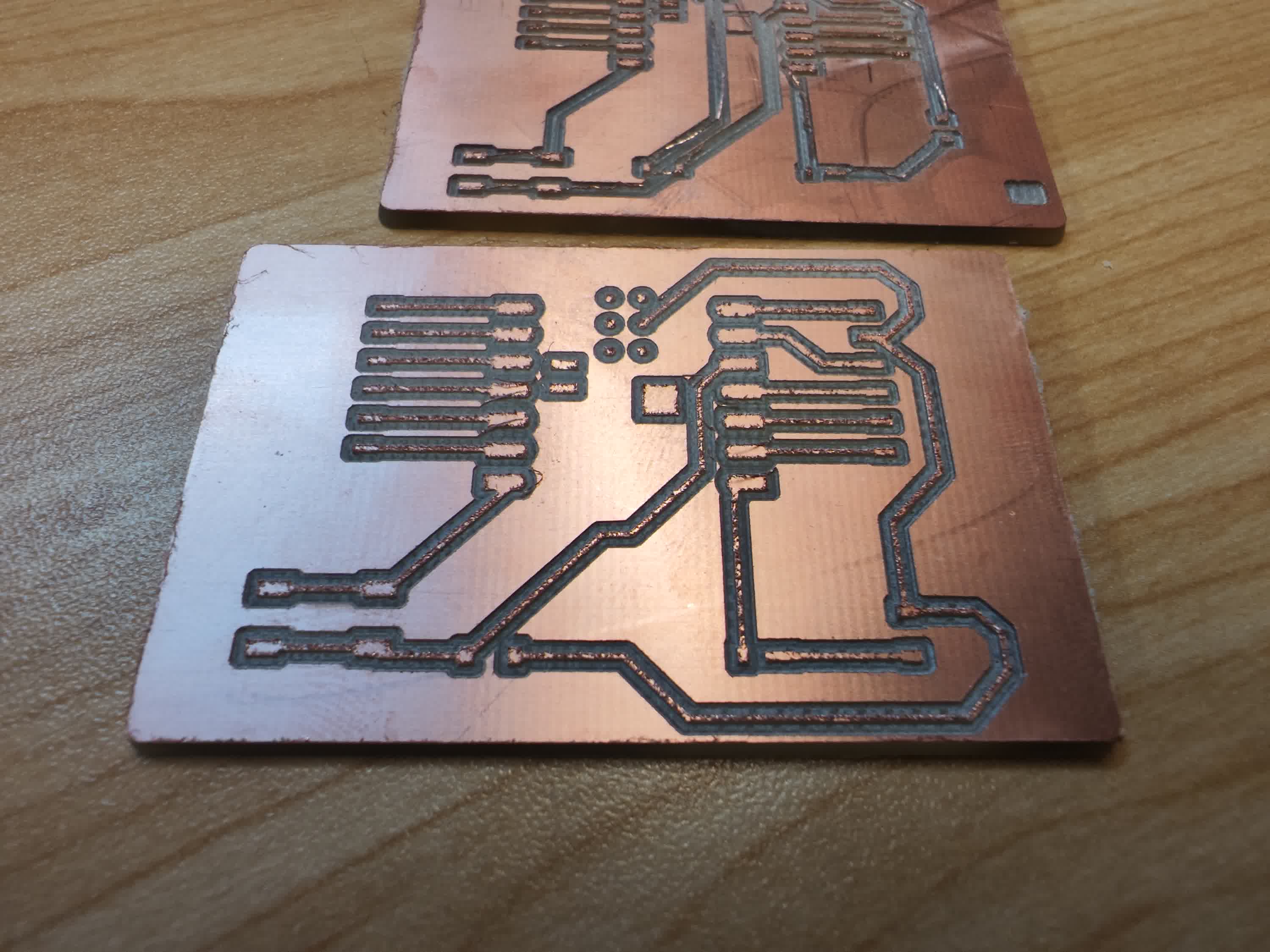
I pried the finished board from the adhesive tape on the bed. Now I have the first cutted copper board, I can significantly see the flaws of the board without testing with a multimeter, since some copper traces are broken physically.
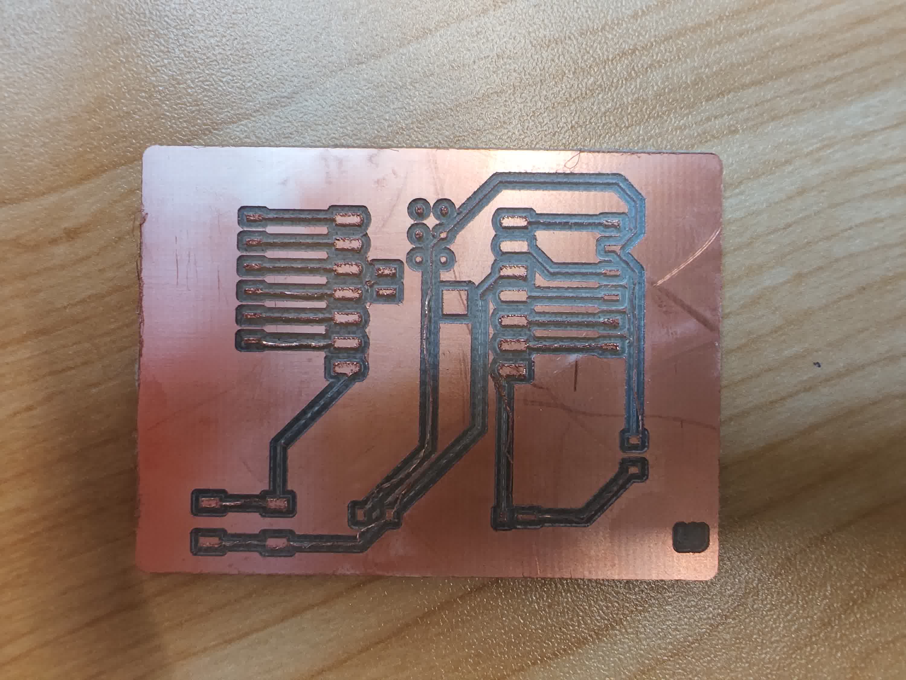
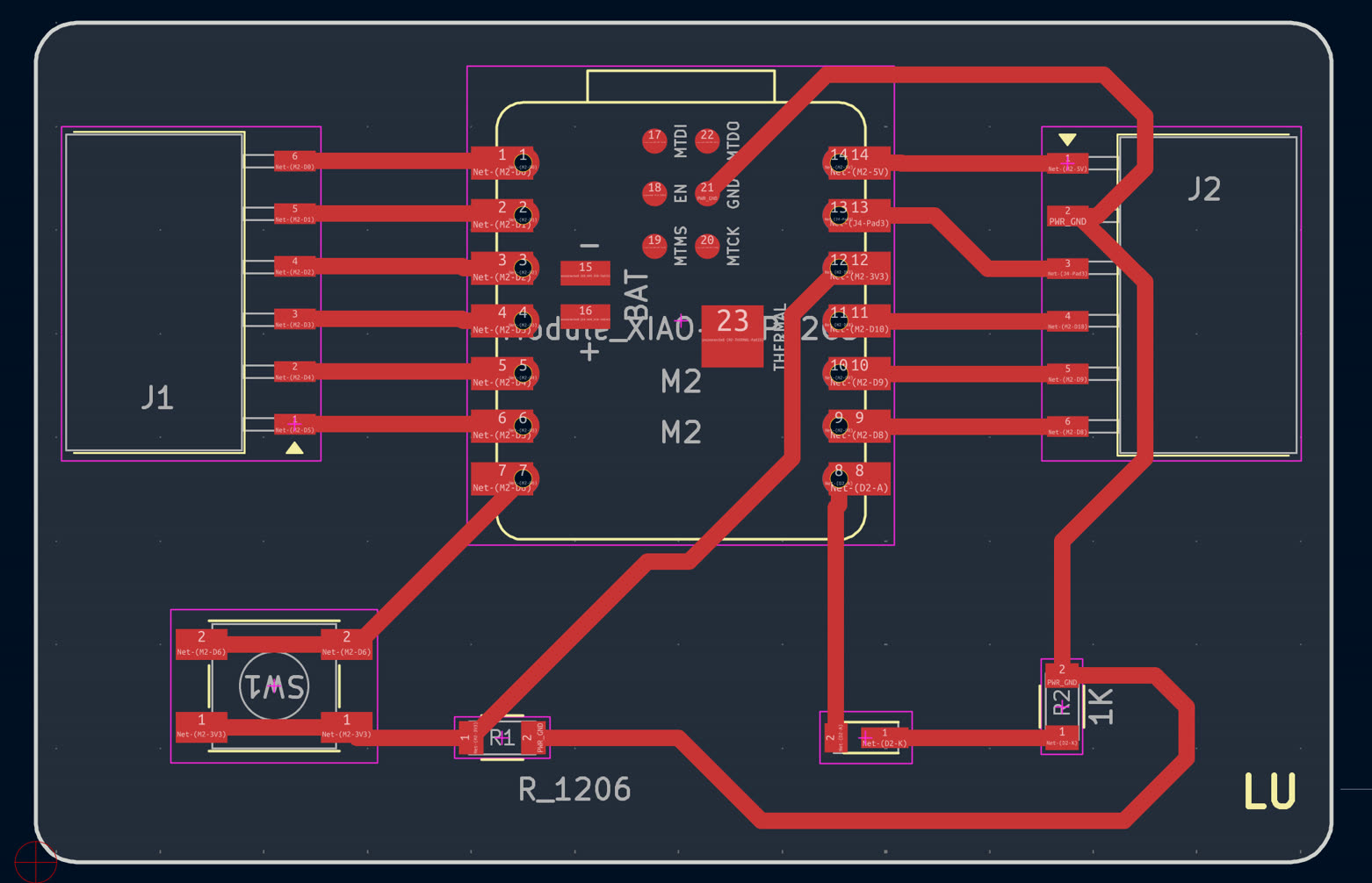
I checked the reason. It is mainly because the setting of the trace width was 0.5mm, too thin to have strong traces. Then I started to fix the setting of the width to 0.8mm as some other Fab Academy fellows succeeded on this, and I redrew the PCB design again (More details were indicated in Week 6--Update).
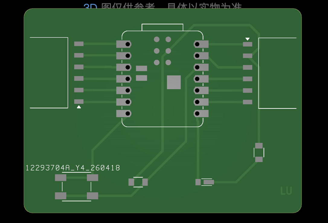
So, after fixing, I have the updated PCB design as below:
I reworked the copper-clad board cutting again, by using the updated PCB design. The second board seemed much better, without any broken lines visually.
Continuity Test
The final step involved a physical inspection: I performed a continuity test with a multimeter to ensure there were no "copper bridges" or short circuits between the traces.
I soldered the XIAO ESP32C3 and the compoents onside.
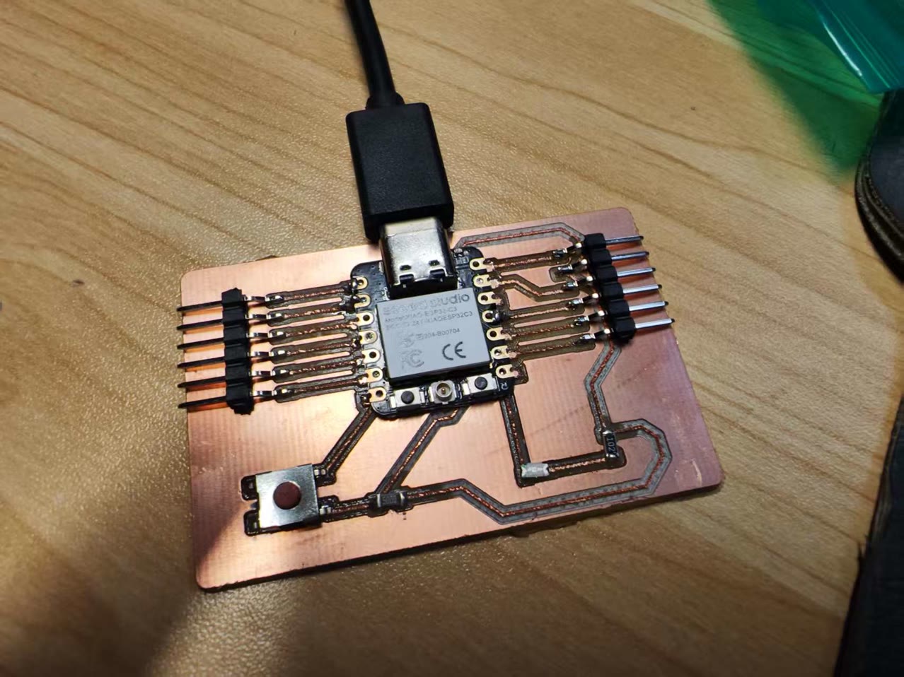
I connected to the computer using USB cable. I asked Cursor to motivate Arduino CLI to write and run code, which indicated "when push the button (D6), the LED (D7) on; when release the button, the LED off".
The code below which activated my hardware:
/*
Seeed XIAO ESP32C3 — button on D6, LED on D7
Hold button: LED on. Release: LED off.
 *
Default: button ties D6 to GND when pressed (INPUT_PULLUP → LOW = pressed).
If your button connects to 3V3 when pressed, set BUTTON_PRESSED_IS_LOW false.
 *
LED: many boards sink current (LED on when pin LOW). Flip LED_ON_IS_LOW if needed.
 */

#include "driver/gpio.h"

#ifndef D6
#define D6 21
#endif
#ifndef D7
#define D7 20
#endif

static const uint8_t BUTTON_PIN = D6;
static const uint8_t LED_PIN = D7;

// Button: true if digitalRead() is LOW when physically pressed
static const bool BUTTON_PRESSED_IS_LOW = true;

// LED: true if LED is on when GPIO is LOW
static const bool LED_ON_IS_LOW = true;

static void ledSet(bool on) {
  const bool lowMeansOn = LED_ON_IS_LOW;
  if (on) {
    digitalWrite(LED_PIN, lowMeansOn ? LOW : HIGH);
  } else {
    digitalWrite(LED_PIN, lowMeansOn ? HIGH : LOW);
  }
}

static bool isPressed() {
  int v = digitalRead(BUTTON_PIN);
  return BUTTON_PRESSED_IS_LOW ? (v == LOW) : (v == HIGH);
}

void setup() {
  gpio_reset_pin((gpio_num_t)BUTTON_PIN);
  gpio_reset_pin((gpio_num_t)LED_PIN);
  pinMode(BUTTON_PIN, INPUT_PULLUP);
  pinMode(LED_PIN, OUTPUT);
  ledSet(false);
}

void loop() {
  ledSet(isPressed());
}
It's working!