Assignment Overview
This week is all about electronics. For the group assignment, our goal was to learn how to use the testing equipment in the lab, like multimeters and oscilloscopes, to check if our boards work correctly. For the individual assignment, I need to use EDA software to design my own microcontroller board, add a few components, and then fabricate and test it.
Group Assignment: Testing Electronic Equipment
This is the link of our group work: https://fabacademy.org/2026/labs/chaihuo/docs/week6/week6_group_assignment/
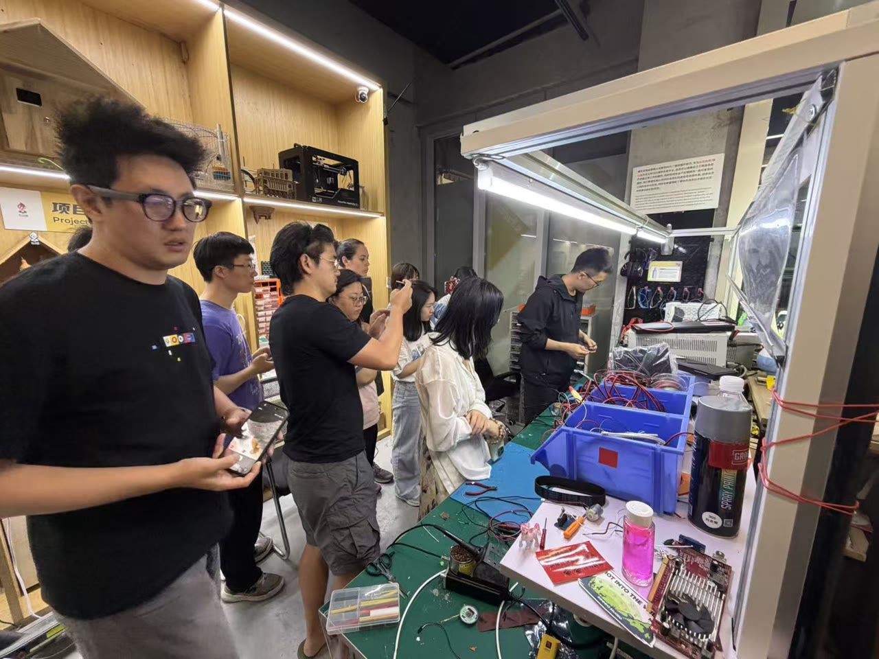
Before we started designing, we spent time learning how to use the tools that help us "see" what’s happening inside the circuits. We focused on learning how to use a multimeter to check connections and an oscilloscope to observe signals.
Understanding the Multimeter
What is a Multimeter?
A multimeter is like a doctor’s stethoscope for electronics. It’s a tool that can measure different things like voltage, resistance, and current. We use it to make sure our board is getting power and, more importantly, to check if there are any short circuits that could burn the chip.
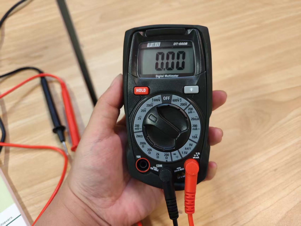
Our Device: CEM DT-660B
In our lab, we used the CEM DT-660B. It’s a small, simple digital multimeter that’s great for beginners because it doesn't have too many confusing buttons.
How the Interface Works: The device has two probes: a Black probe that always goes into the COM port (Ground), and a Red probe that goes into the other port for measuring voltage and resistance.
Here is what the dial settings mean for our tasks:
V⎓ (DC Voltage): We use this to check the battery or USB power. We usually set it to 20 to measure our 5V or 3.3V boards.
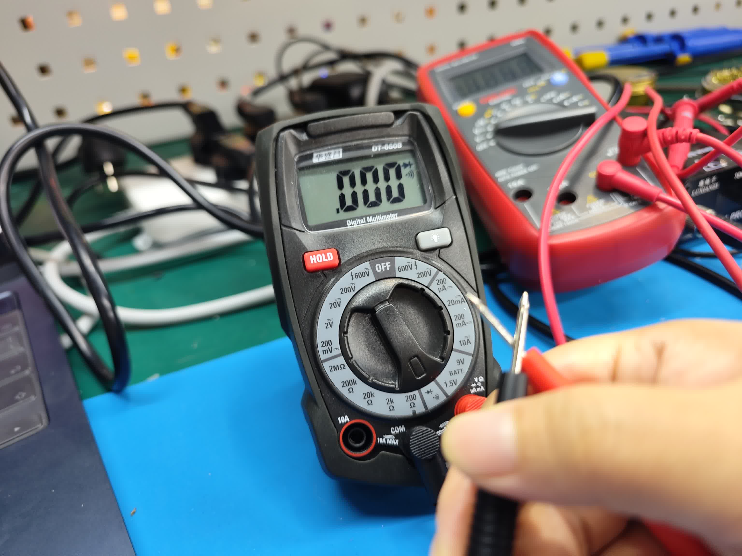
Continuity Buzzer: It looks like a wifi signal with an arrow. This is our most-used setting. When we touch the two probes together, it makes a "beep" sound. We use this to touch different points on our PCB; if it beeps when it shouldn't, we know there is a short circuit. For example, I connected the head of black and red probes, it showed 000 on the screen.
Ω (Resistance): We use this to check if our resistors have the right value or if a connection has too much resistance.
V~ (AC Voltage): This is for wall outlets. Since we only work with low-voltage DC boards, we don't use this setting in the lab.
A⎓ (Current): This measures how much power the board is consuming, though we have to be careful not to blow the fuse when using it.
Testing Procedures: Multimeter in Action
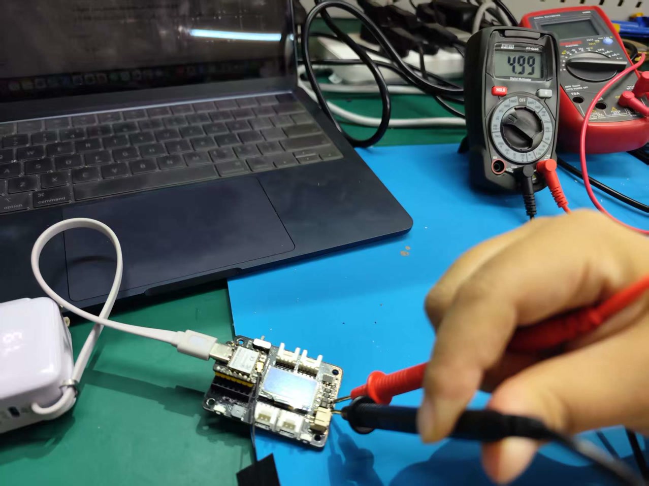
After getting familiar with the digital multimeter CEM DT-660B, we used it to test our XIAO ESP32C3 and the XIAO Expansion Board. Here is exactly what we did:
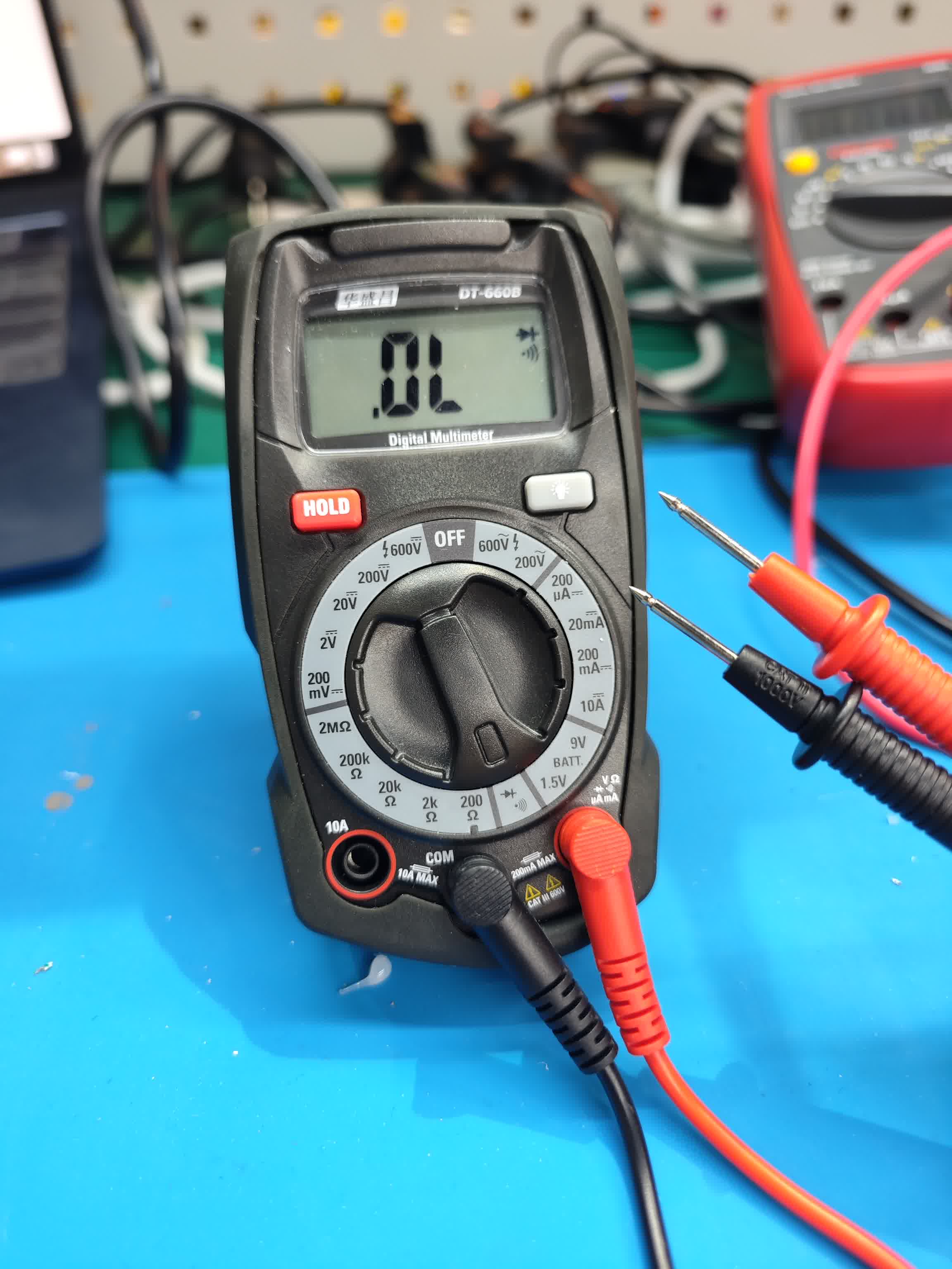
- Continuity Test (Checking for Shorts) Before powering up, we had to make sure the board wouldn't short-circuit. We set the multimeter to the Continuity mode (Buzzer). We touched the red probe to VCC/5V and the black probe to GND.
Result: The multimeter did not beep, and the screen displayed "OL" (Over Load). This means the resistance is infinite and there is no direct connection between power and ground. It was safe to proceed.
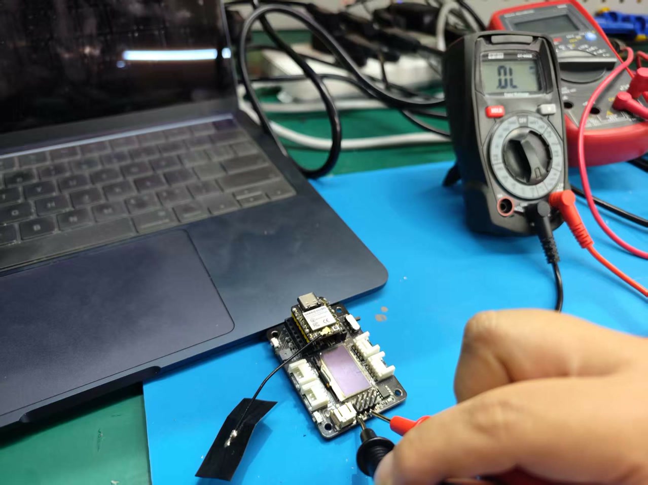
- Measuring Input Voltage (5V) Instead of using a computer USB port, I used a power bank to power the board. We switched the multimeter to DC Voltage (20V range) to check the input.
Result: The screen displayed 4.99V. We analyzed this and concluded that the tiny 0.01V drop is normal. It's likely caused by the conversion loss inside the power bank's boost circuit and the resistance of the USB cable we used.
- Measuring System Voltage (3.3V) Next, we measured the regulated voltage that powers the ESP32C3 chip. We moved the red probe to the 3V3 pin.
Result: The multimeter showed 3.34V.
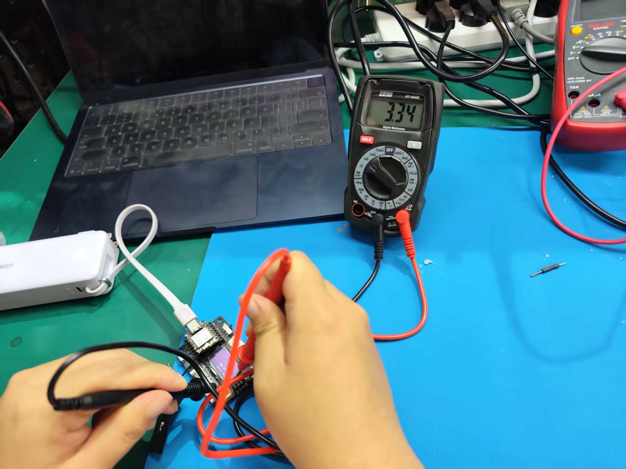
Analysis: This is slightly higher than 3.30V but well within the safe operating range (typically typically 3.3V±5%). We think this happens because the power bank provides a very "strong" 5V input, and the voltage regulator on the expansion board is highly efficient. This 3.34V ensures the chip stays stable even if we connect more sensors later.
Understanding the Oscilloscope
The oscilloscope is like a "video camera" for electricity. While a multimeter shows a single number, the oscilloscope shows how voltage changes over time as a live waveform.
Key Measurements and Their Importance
During our testing with the oscilloscope, we focused on the following key values. These will be my main "tools" for debugging future projects:
Click the image to view the sheet.Testing Procedures: Oscilloscope
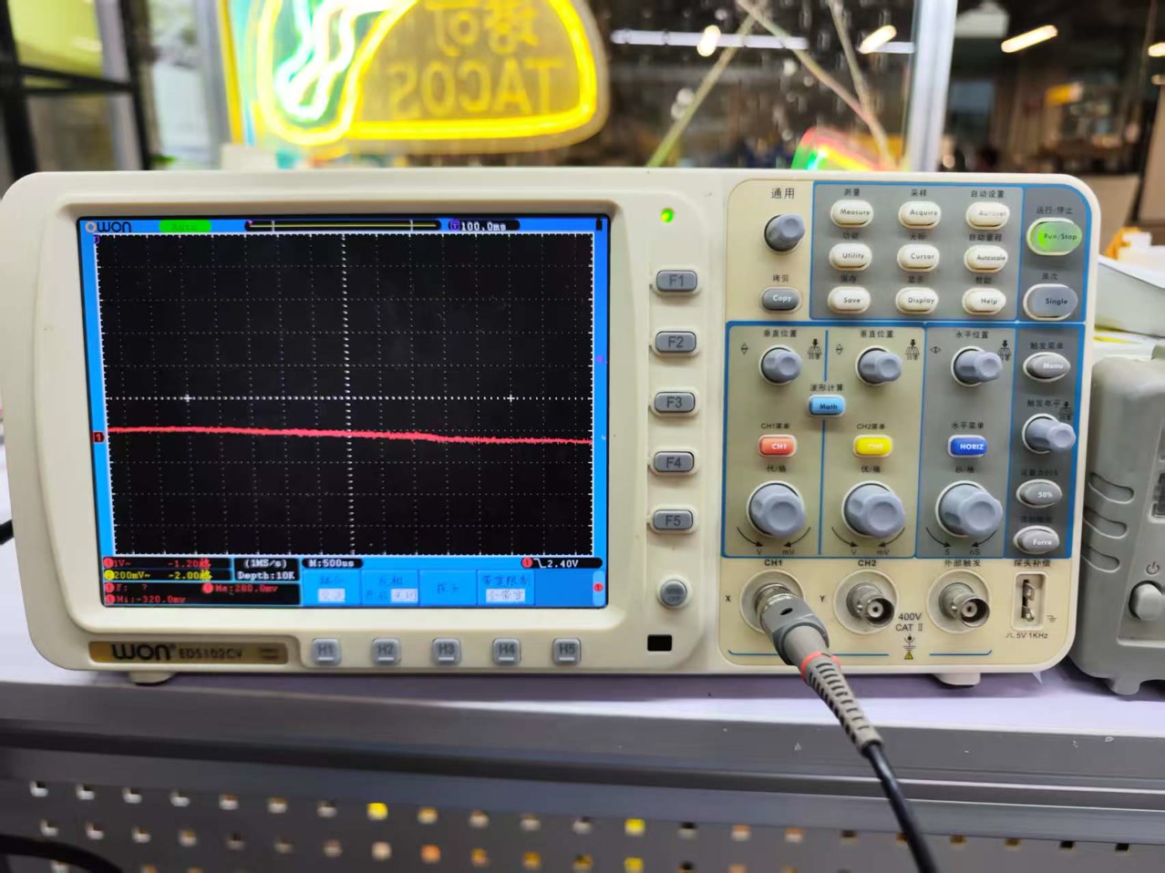
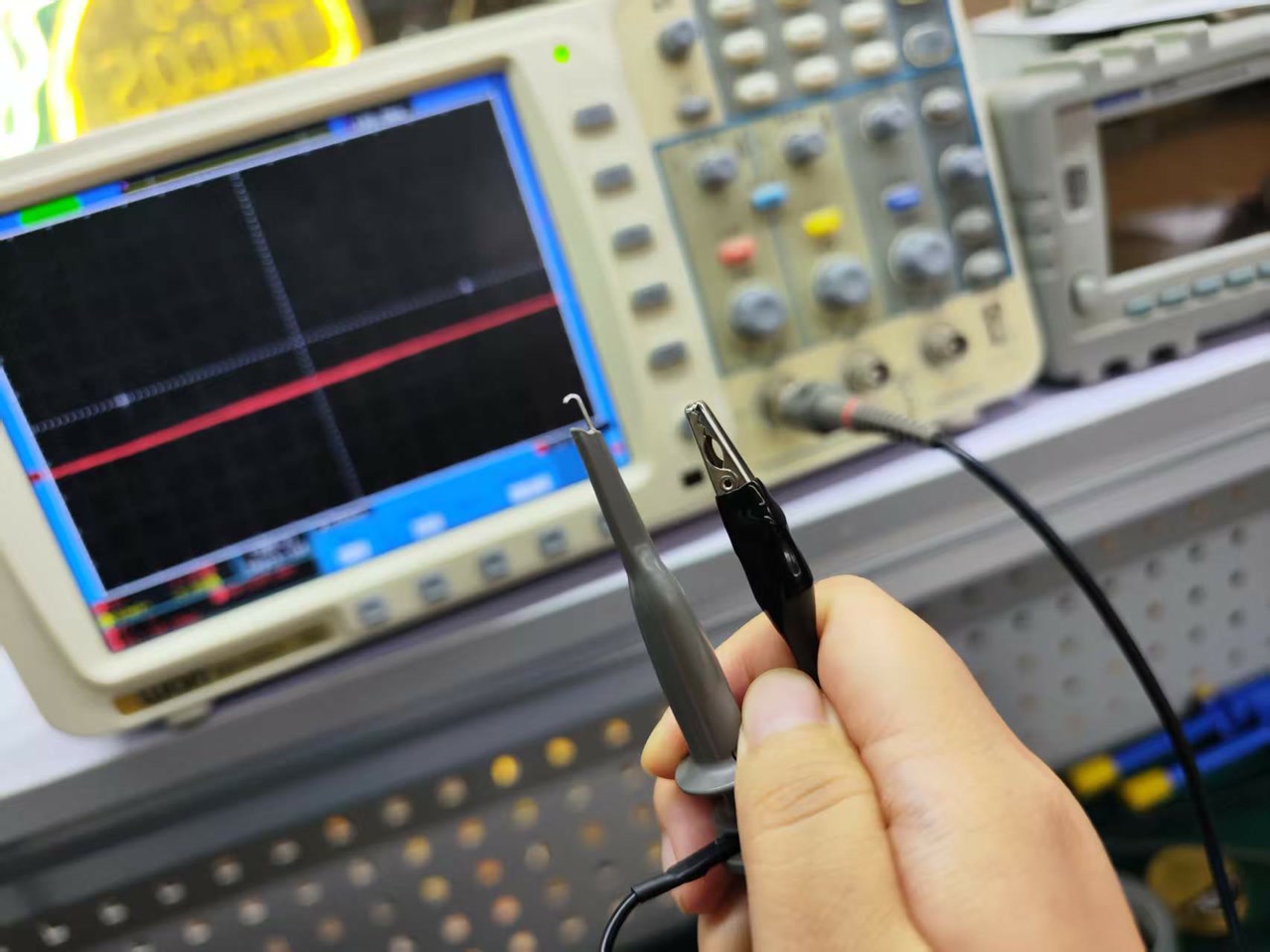
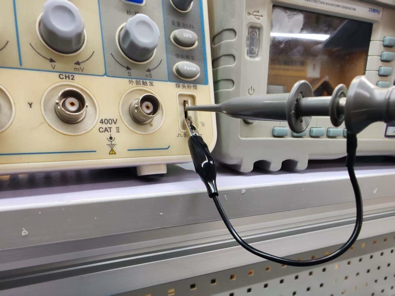
We used the OWON EDS102CV to visualize the voltage over time. To learn the machine, we used its built-in Probe Comp (Calibration) signal.
-
Connected the probe hook to the ~5V/1kHz terminal and the black ground clip to GND.
-
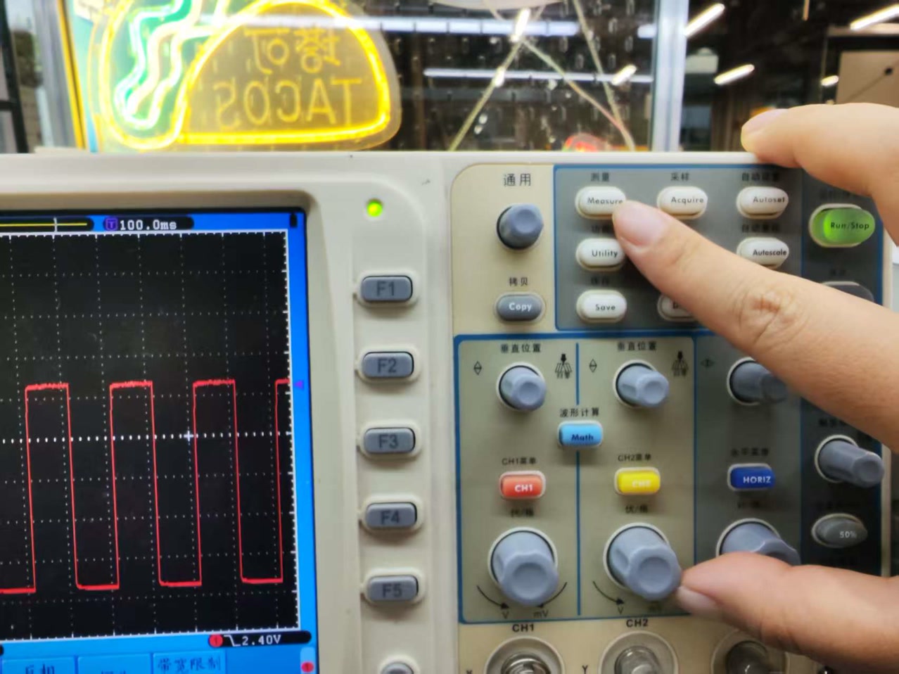
Pressed the [Autoset] button on the right side to automatically stabilize the waveform.
-
Enabled the [Measure] menu to see the precise data of the signal by pressing "measure" button on the right, and press the button H1 below "add measurement". Then I pressed F3 button to see all the data.
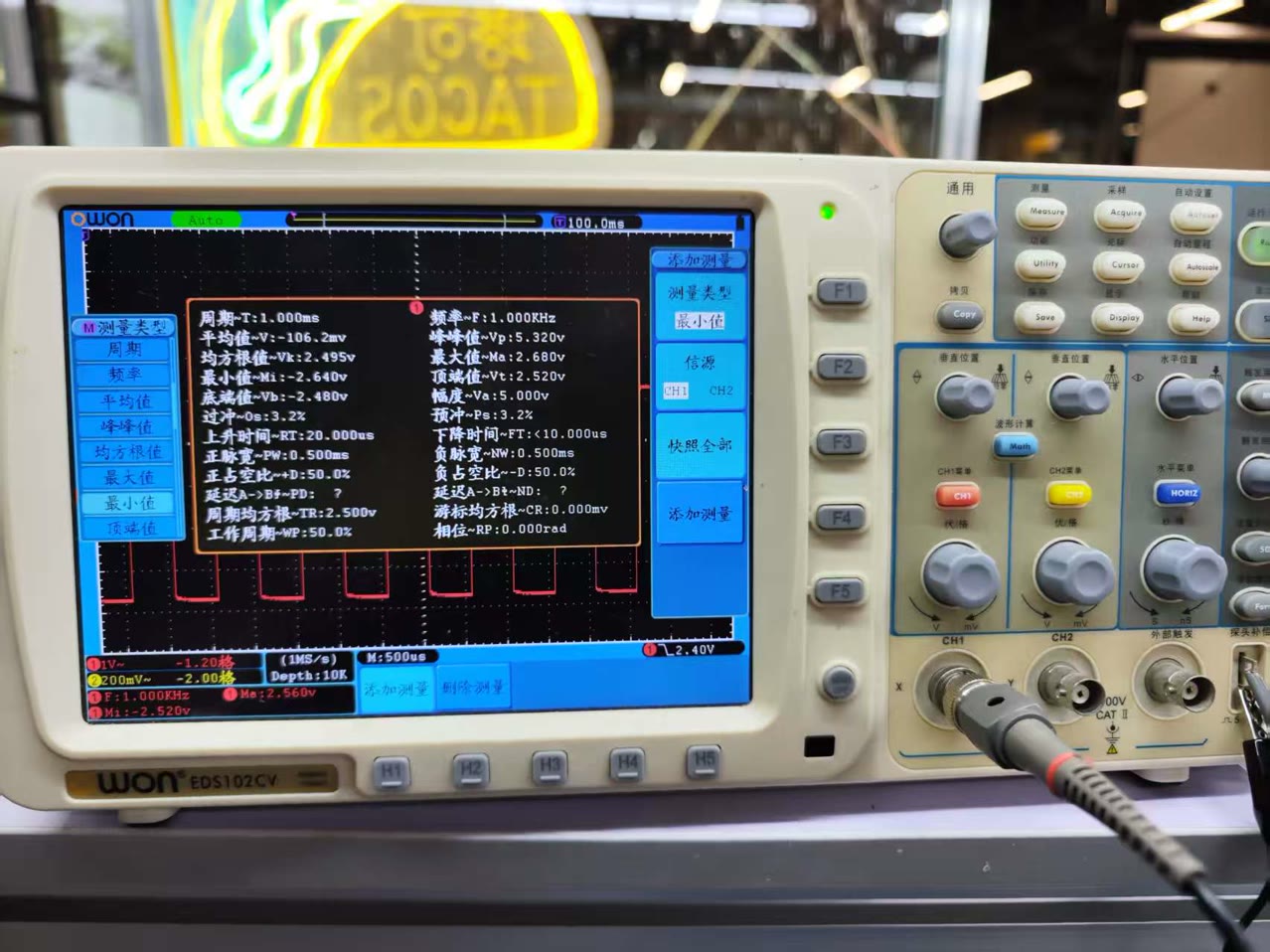
Data Observation & Analysis:
We observed a clean square wave and recorded the following measurements:
Frequency: 1.000kHzThis means the signal pulses exactly 1,000 times per second. It matches the "1kHz" label on the terminal, proving the oscilloscope's internal clock is accurate.
Period: 1.000msThe period is the time it takes for one full cycle. Since $f = 1/T$, a 1kHz frequency means the period should be 1ms. Our measurement was perfect.
Peak-to-Peak (PK-PK, Vpp): 5.080VThe voltage jumps from 0V to 5.080V. This 1.6% deviation from 5V is very small and well within the acceptable error range for this equipment.
The meaning to us of these key measurements:
By learning these parameters, I now have eyes to see what’s happening inside my circuits:
- Safety: I can check the Vpp to make sure I don’t connect a 5V sensor to a 3.3V pin by mistake.
- Communication: I can use Frequency to see if my sensors are actually talking to my microcontroller.
- Debugging: If my board acts "crazy," I can look at the Waveform to see if the power is "dirty" (noisy) and needs a capacitor to smooth it out.
Reflection: Multimeter vs. Oscilloscope
I learned that these two tools complement each other:
- I use the Multimeter for quick "static" checks, like finding short circuits or verifying the main power supply (4.99V and 3.34V). It gives me a reliable number to confirm the board is safe.
- I use the Oscilloscope for "dynamic" analysis. It allows me to see how the voltage behaves over time. For example, it confirmed my 1kHz signal was stable and helped me understand the relationship between Frequency and Period. In the future, if my board has power issues, I’ll reach for the multimeter first. If my communication or sensors aren't working, I'll use the oscilloscope to "see" the data flow.
Individual Assignment: PCB Design
The objective of this week is to move from pre-made commercial expansion boards to designing my own custom PCB. I will be designing a functional microcontroller board that facilitates interaction through physical inputs and outputs.
My workflow involves:
- Researching and selecting a suitable EDA tool.
- Designing a custom PCB that integrates an XIAO ESP32C3 with an LED (output) and a push-button (input).
- Utilizing the Fab Electronics Library to ensure component compatibility with our lab's inventory.
- Finalizing the board layout for production and validating the communication capabilities (Wi-Fi/Bluetooth) of the ESP32C3.
1. Research on EDA Tools
To select the most suitable software for my electronics design, I explored several industry-standard EDA (Electronic Design Automation) tools. Here is my analysis based on their features, accessibility, and learning curves:
A. Autodesk Fusion Electronics (formerly Eagle)A widely used tool in the maker community, now integrated into the Autodesk Fusion 360 ecosystem.
- Strengths: It offers a seamless transition between 2D PCB design and 3D modeling. If you design a case in Fusion 360, the PCB updates automatically.
- Weaknesses: The interface can be cluttered for beginners, and the free version has limitations on board size and the number of layers. B. Altium Designer
The professional industry standard for high-end, complex multi-layer PCB design.
- Strengths: It has an incredibly powerful routing engine, advanced simulation capabilities, and centralized library management.
- Weaknesses: It is extremely expensive (prohibitive for individual students) and only runs natively on Windows. The learning curve is very steep for a one-week project. C. Tinkercad Circuits
A browser-based simulation tool aimed at beginners and educators.
- Strengths: Excellent for simulating Arduino code and basic breadboard circuits without risking hardware damage.
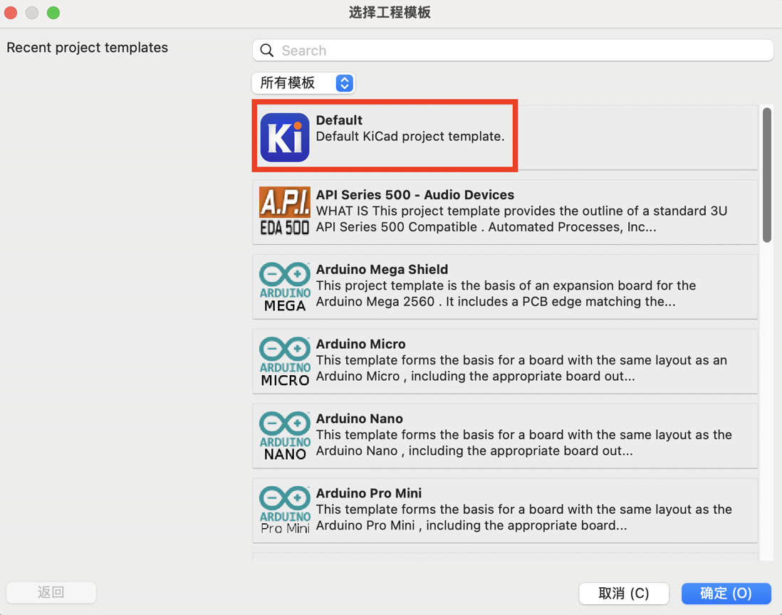
- Weaknesses: It is not a true PCB design tool. You cannot generate the Gerber files or professional footprints required for CNC milling or industrial production. D. KiCad (The Chosen Tool)
A powerful, cross-platform, open-source suite for EDA.
- Strengths: * Open Source, no licensing fees or "paywalls" for advanced features. --Fab Ecosystem: It has the best support within the Fab Academy network. The Fab Electronics Library is specifically optimized for KiCad, ensuring the footprints match our lab's inventory perfectly.
--Logic: The workflow (Schematic -> Footprint Assignment -> PCB Layout) is very logical and easy to debug.
2. Why I Chose KiCad
After comparing the options, I decided to proceed with KiCad 10.0 for the following reasons:
- Inventory Alignment: The availability of the fab.kicad_sym and fab.kicad_mod libraries means I don't have to spend hours searching for or creating footprints. I can be 100% sure that the resistor or button I pick in the software exists in our lab's drawer.
- Community Support: Fab Academy has a vast archive of KiCad tutorials. If I encounter an error during routing or DRC (Design Rule Check), there is a high probability that the solution is already documented in the Fab community.
- No Limits: Unlike the free versions of commercial software, KiCad allows me to design boards of any size or complexity without restrictions.
3. Installation and Environment Setup on KiCad
- Download and install KiCad 10.0.0. I went to website kicad.org/download/macos/ and download it to my computer.
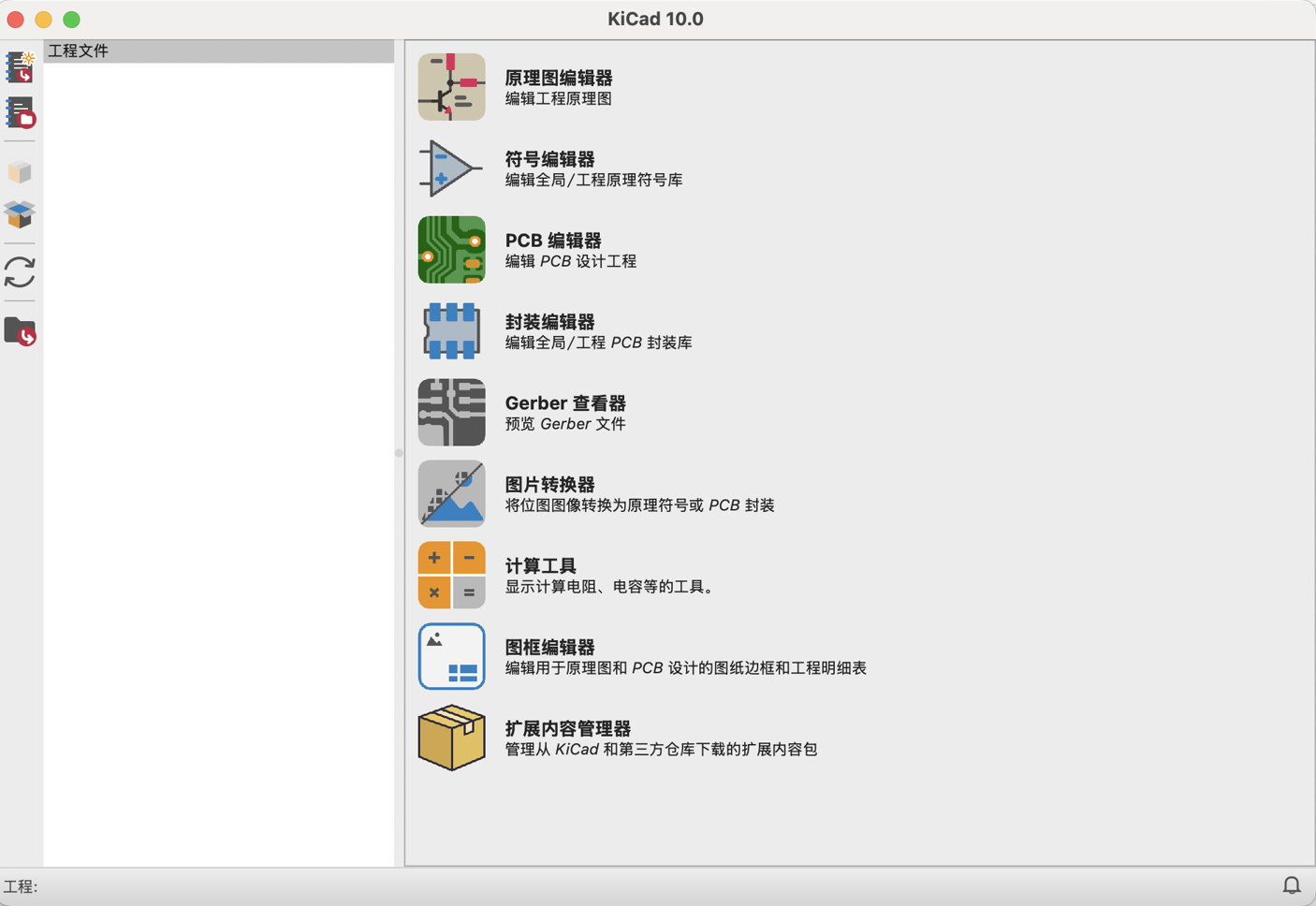
After downloading and installation, I got access to my KiCad on my computer.
-
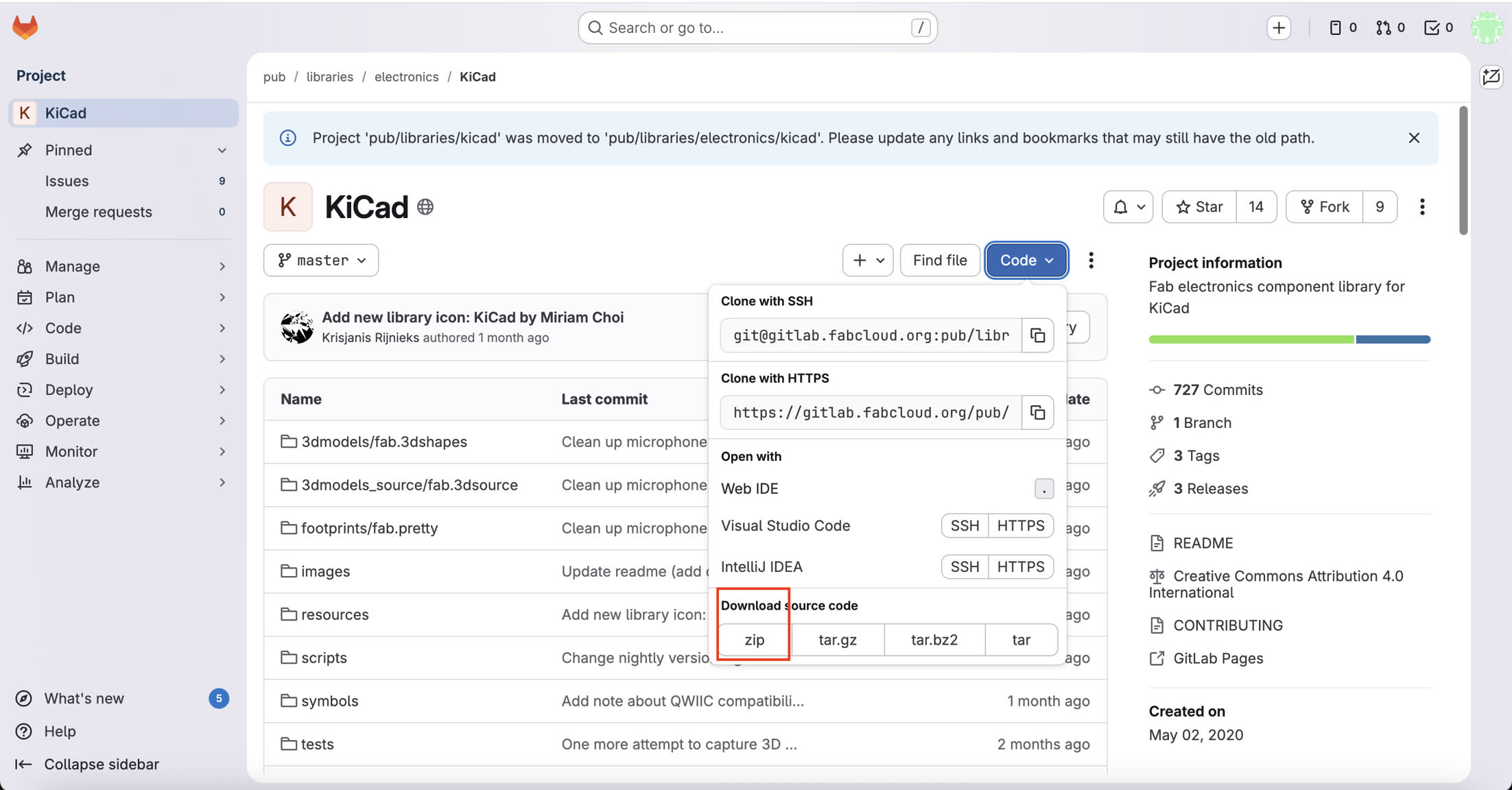
I downloaded the Fab Electronics Library from the GitLab repository and extracted the files to a permanent local directory.
-
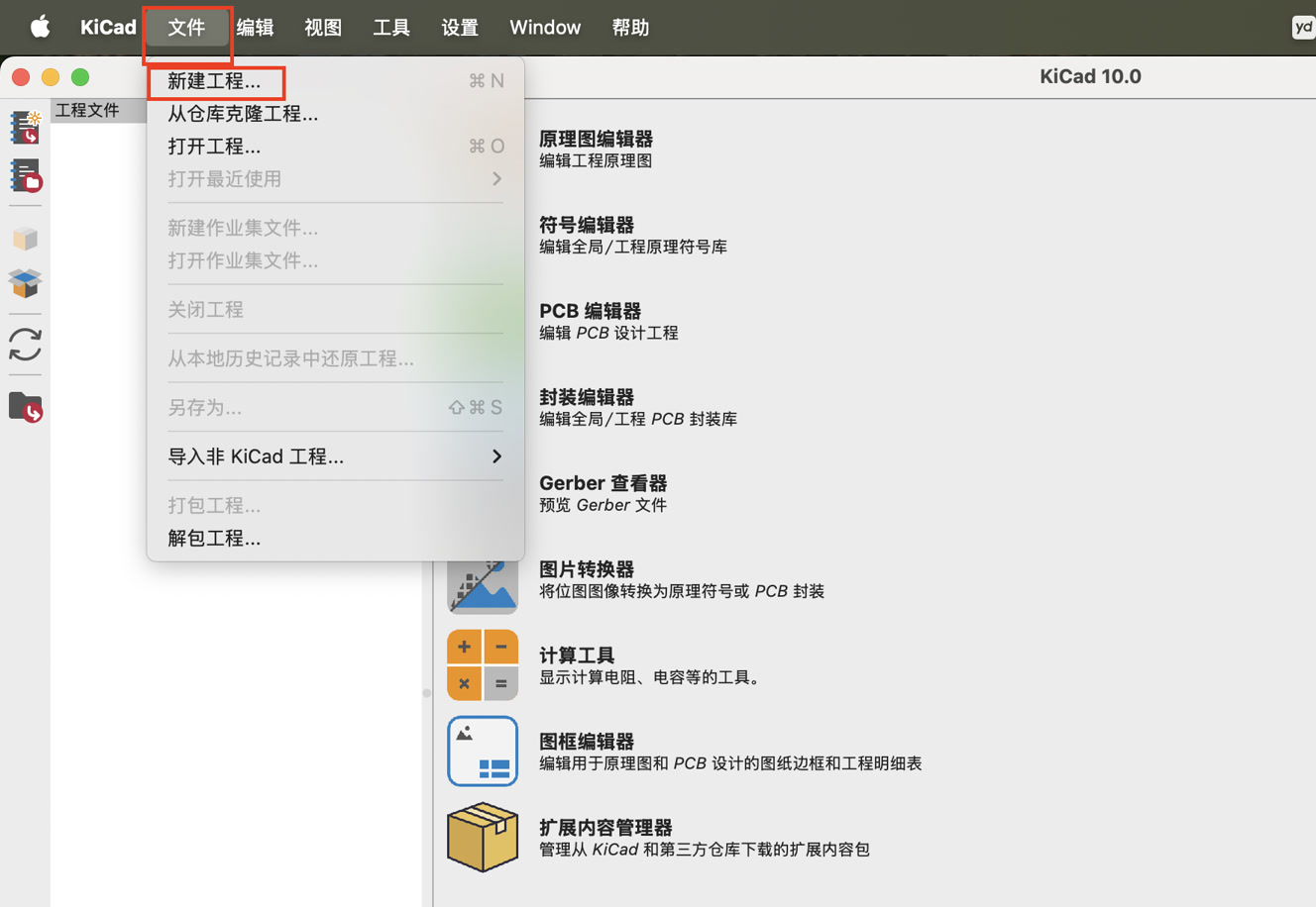
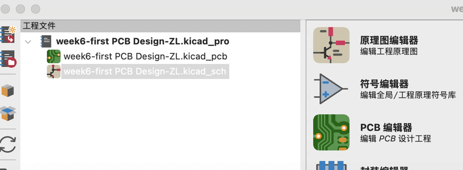
I navigated to File > New Project to set up a dedicated workspace for my design.
-
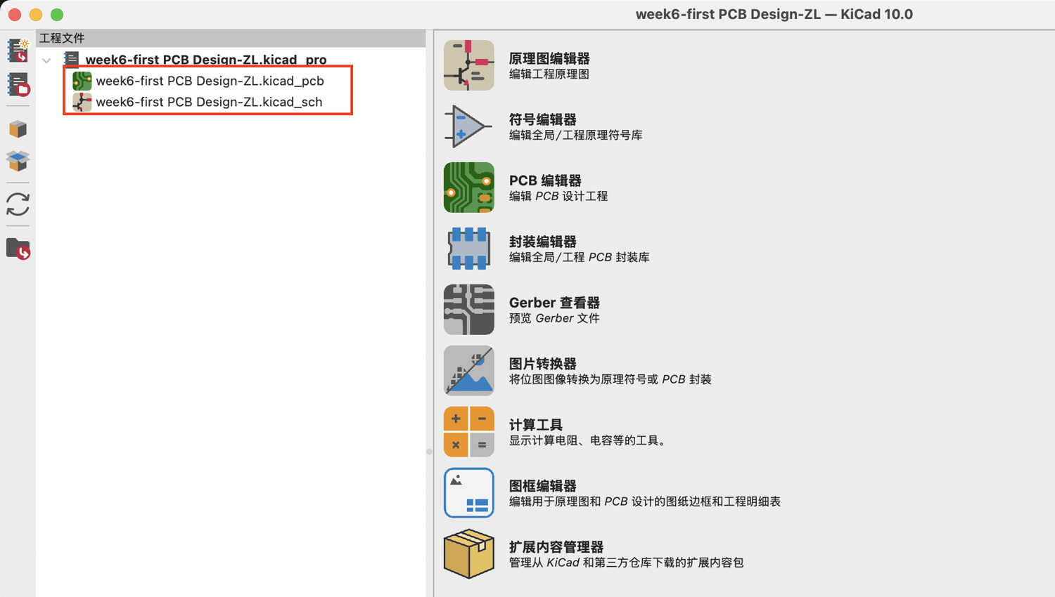
I created a new folder named "week6-first PCB Design" to store all my schematic and PCB layout files in one organized location. Upon saving, KiCad automatically generated the .kicad_pro, .kicad_sch (Schematic), and .kicad_pcb (PCB) files required for the design process.
-
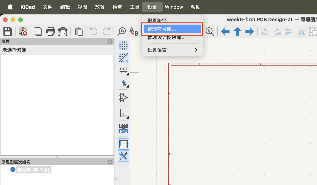
In the Schematic Editor, I navigated to Settings > Manage Symbol Libraries to initiate the library linking process.
-
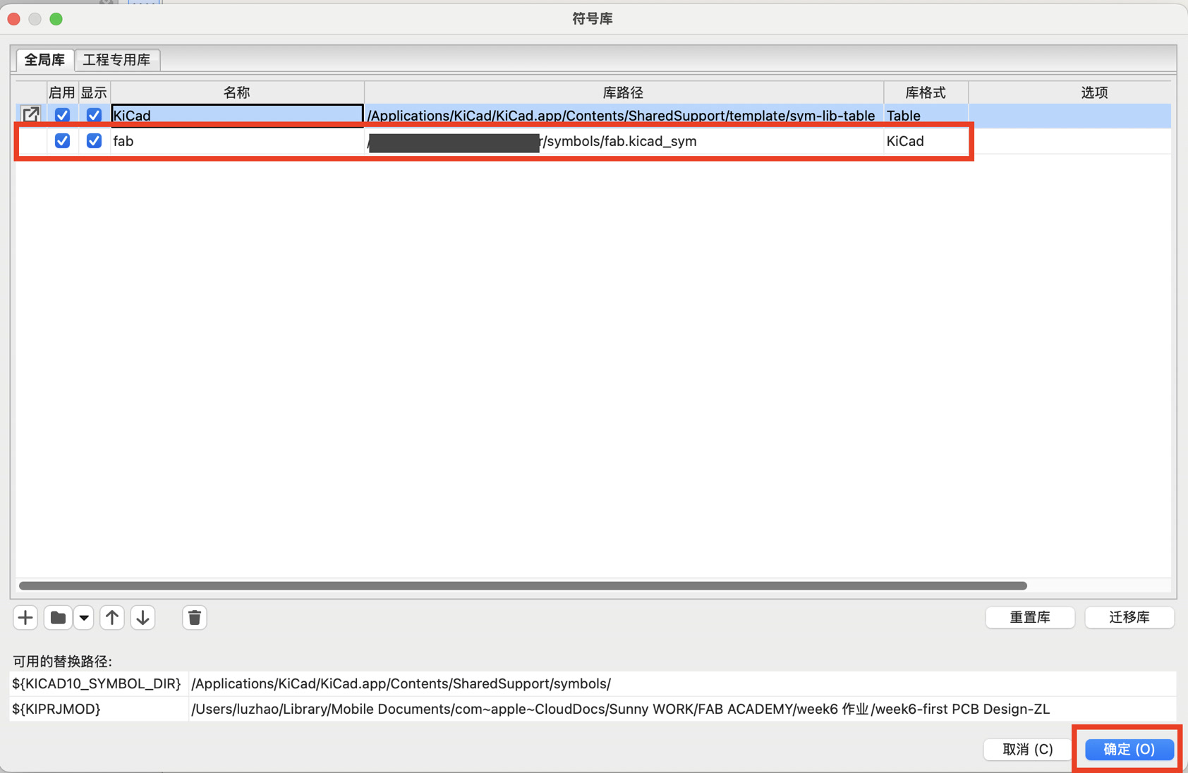
Under the Global Libraries tab, I clicked the "Add existing library to table" icon and selected the fab.kicad_sym file. Then I can see the new library named "fab" in the list.
-
Similar steps to add the footprint library. I switched to the PCB Editor and accessed Settings > Manage Footprint Libraries to configure the physical component shapes. I added the entire fab.pretty folder to the Global Libraries table to ensure all footprints match our lab's physical inventory.
4. Start my PCB Design
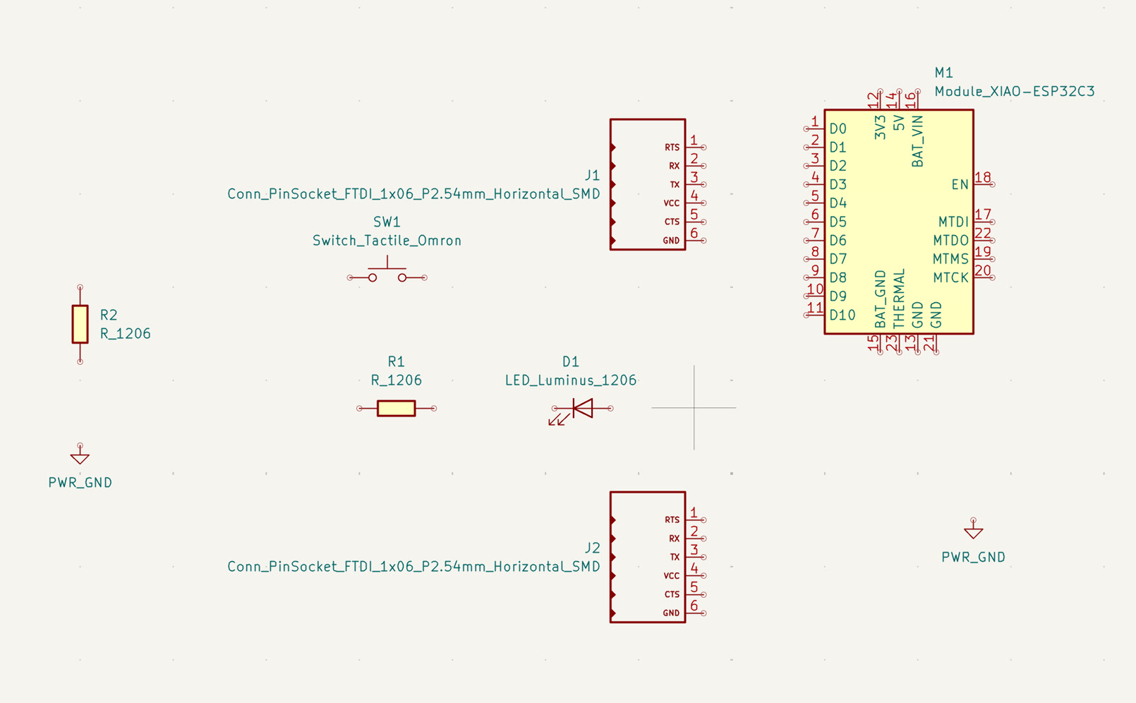
I double clicked "week6-first PCB Design-ZL.kicad_sch" to start my schematic design.
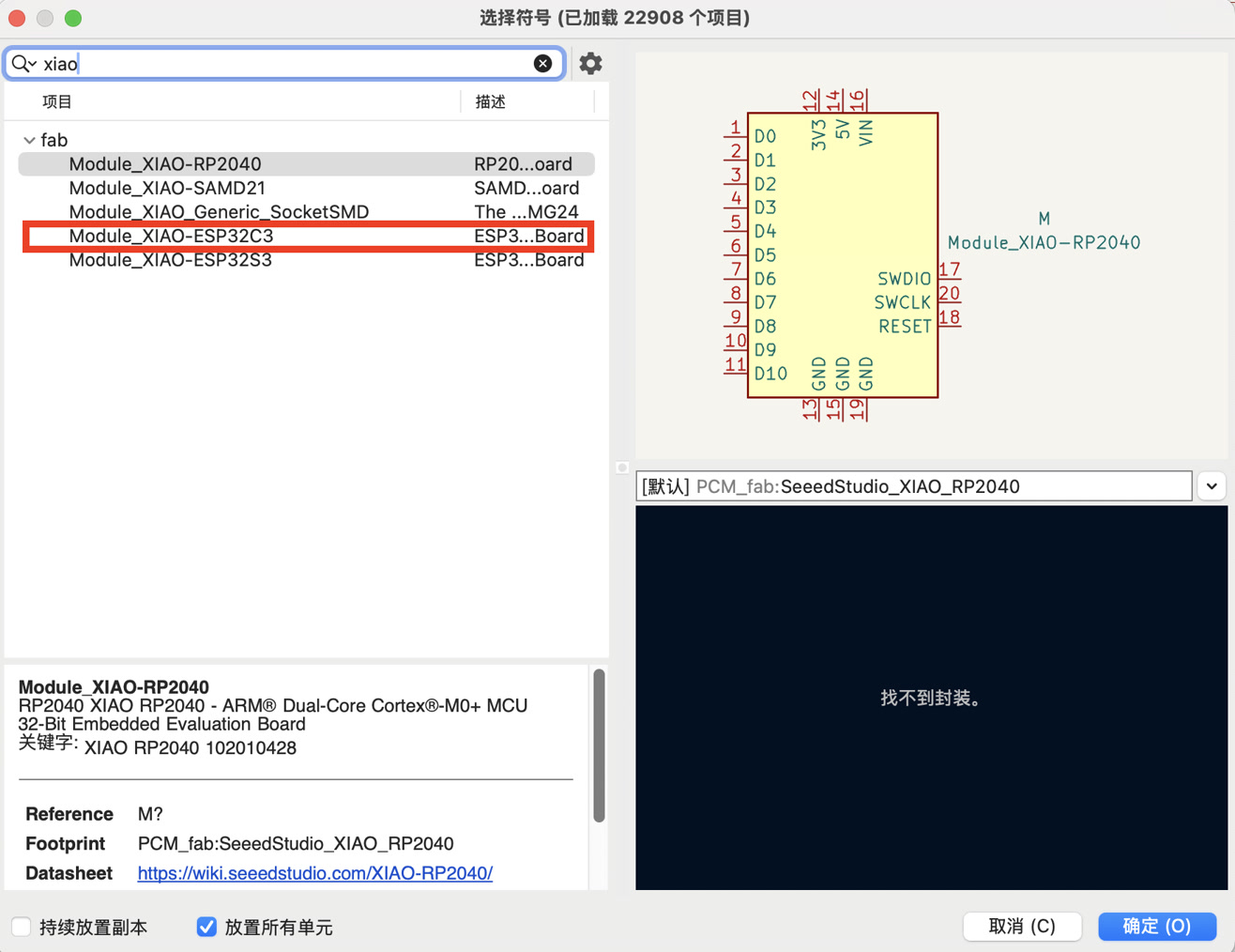
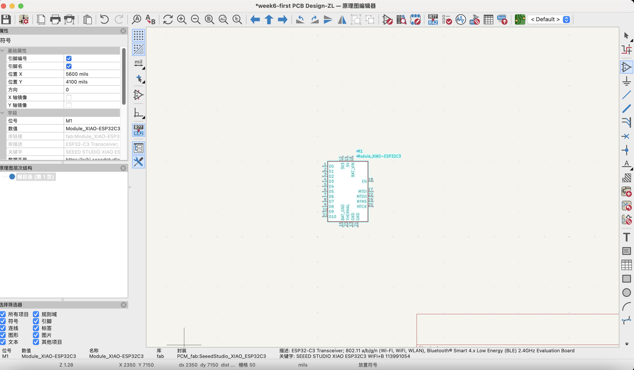
Place Microcontroller: I used the Add Symbol tool (shortcut 'A') to search for and place the Seeed_XIAO_ESP32C3 from the fab library at the center of the canvas.
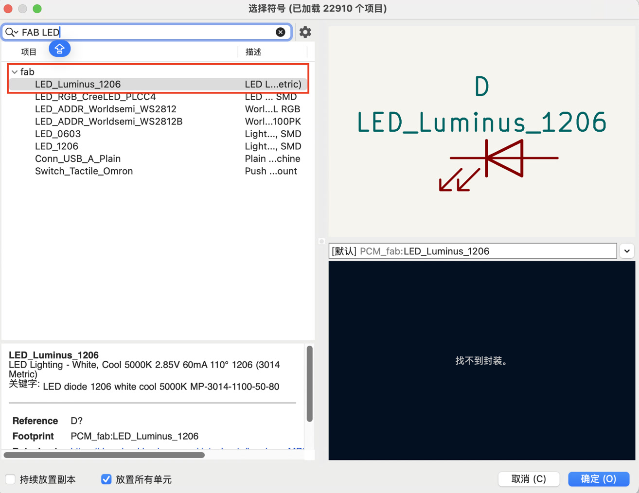
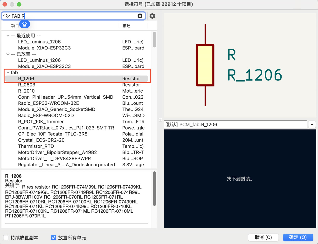
Add Output Component: I placed a fab:LED with a 1206 package, choosing this larger footprint to ensure easier hand-soldering later in the lab.
Add Current Limiter: I added 2 fab:R (resistor) also in a 1206 package to protect the LED and also the switch from excessive current.
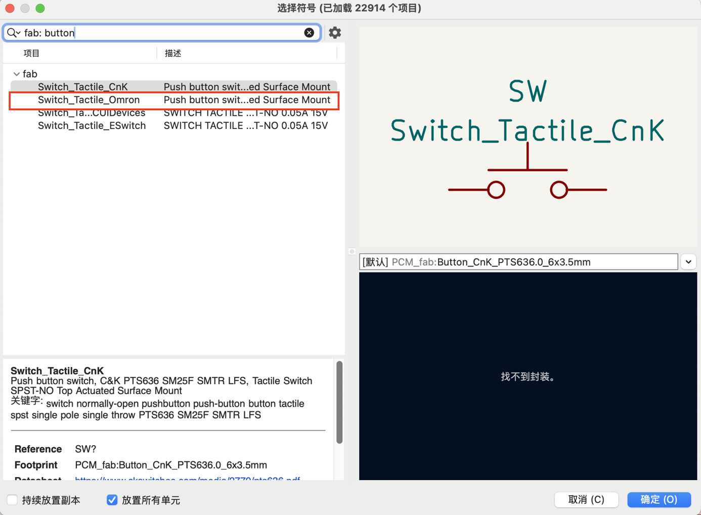
Add Input Component: I searched for and placed the fab:Switch_Tactile_Omron as the physical interaction button.
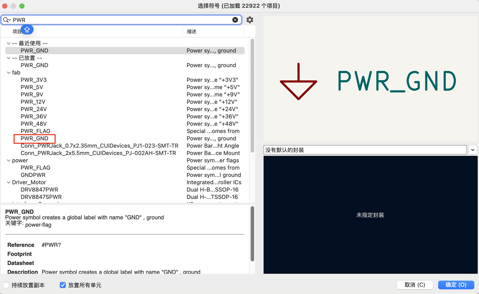
Add Power Reference: I placed 2 PWR GND symbol to define the ground for the entire circuit.
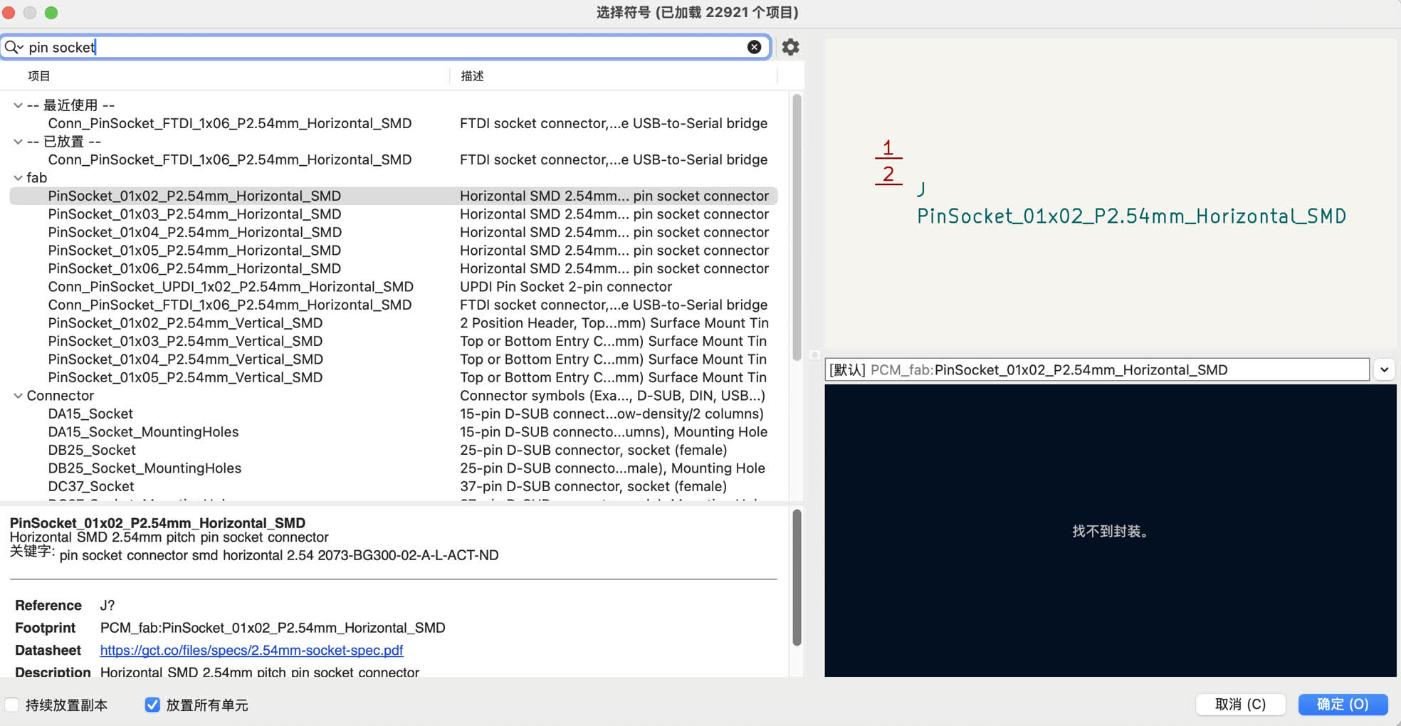
Add Pin Socket: I placed 2 pin sockets (6-pin) to allow the XIAO ESP32C3 to be easily plugged/unplugged and providing access points for external input/output devices.
Then everything I need is on the sheet. I am ready to do the wiring on next step.
5. Hardware Design Logic and Pinout Review
Before proceeding to the physical PCB layout, I performed a thorough review of the Seeed Studio XIAO ESP32-C3 pinout to ensure optimal peripheral connectivity. This review confirmed my design logic and wiring choices from the simulation phase.
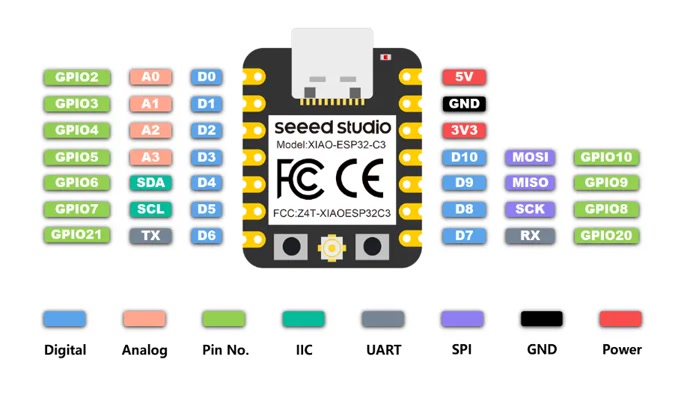
LED Control: I selected D7 (GPIO20) for the LED output because it provides standard digital I/O capabilities suitable for PWM control if needed later.
Button Input: I assigned the Omron tactile button to D6 (GPIO21) to utilize its internal pull-up resistor (INPUT_PULLUP), eliminating the need for an external resistor while ensuring a clean digital signal.
Power Ground: All common ground connections (from the LED and the button) are tied to a designated GND pin on the XIAO to complete the circuit loop.
I also discovered that the four pins of a tactile switch are internally connected in pairs, meaning the top two pins are permanently shorted; therefore, a diagonal wiring configuration is essential to ensure the circuit only closes when the button is physically depressed.
6. Simulation on Wokwi
Wokwi is a useful tool for me to test if the wiring is correct before starting wiring on KiCad. I had used it for Week 4 task, and I will check if it can work directly. The simulation project is simple, when I push the button, the LED turns on, otherwise it turns off.
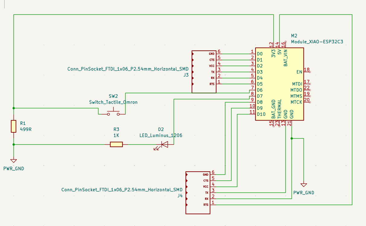
7. Schematic Wiring and Grounding
I used the Wire tool (shortcut 'W').
Pin Socket Integration: I integrated two 6-pin female headers to serve as a modular socket for the XIAO ESP32C3. This design allows the MCU to be easily detached and provides physical access to all pins for future expansion.
LED Circuitry: I connected XIAO D7 to the LED anode, linked the cathode to a 1206 resistor, and finally terminated the path to a PWR GND symbol.
Button Circuitry: I routed a wire from XIAO D6 to the tactile switch and to ensure a reliable switching state, the diagonal lower-right pin is connected to GND, utilizing the internal 1206 resistor of the ESP32C3.
Optimized Grounding: I placed two separate GND symbols in the schematic to avoid long, cluttered wires, as KiCad automatically treats all identical power symbols as a single electrical net.
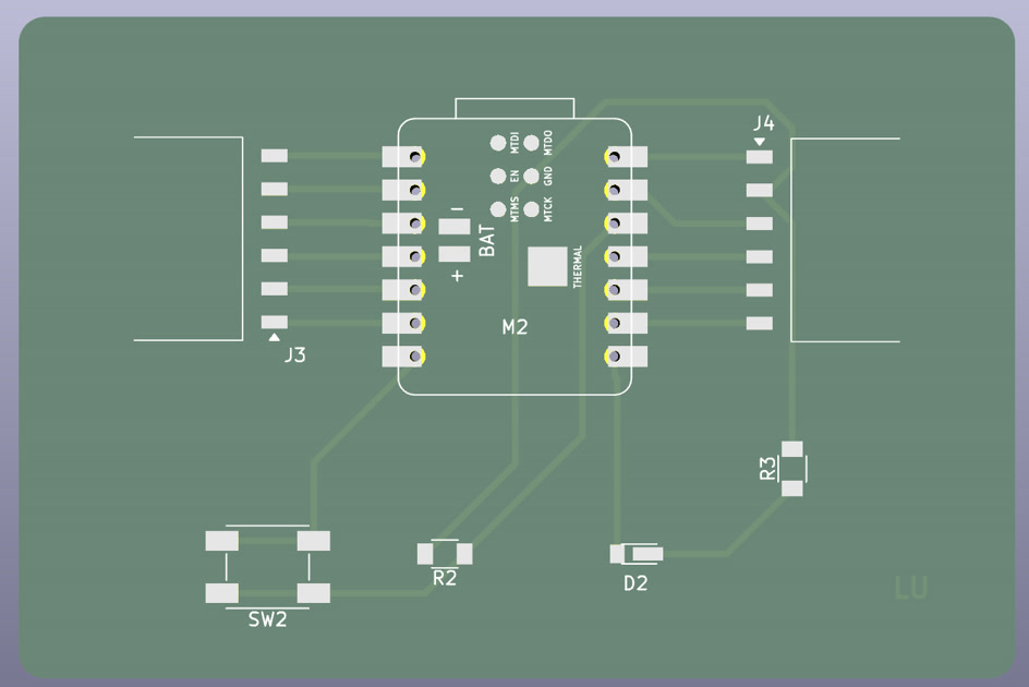
After completing every wiring details, my schematic work is as below:
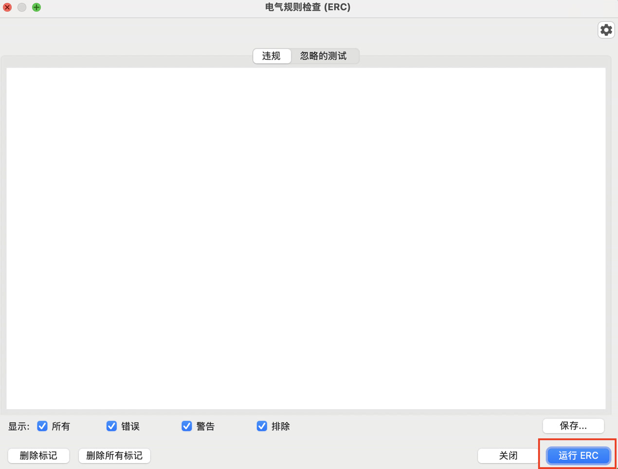
Before transitioning to the PCB layout, I performed an Electrical Rules Check (ERC) to validate the integrity of my schematic.
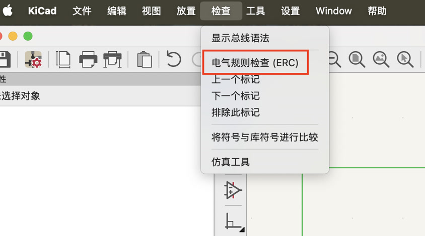
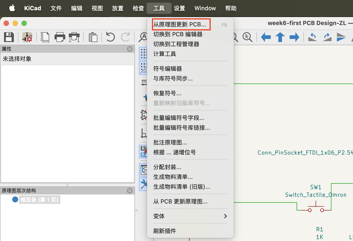
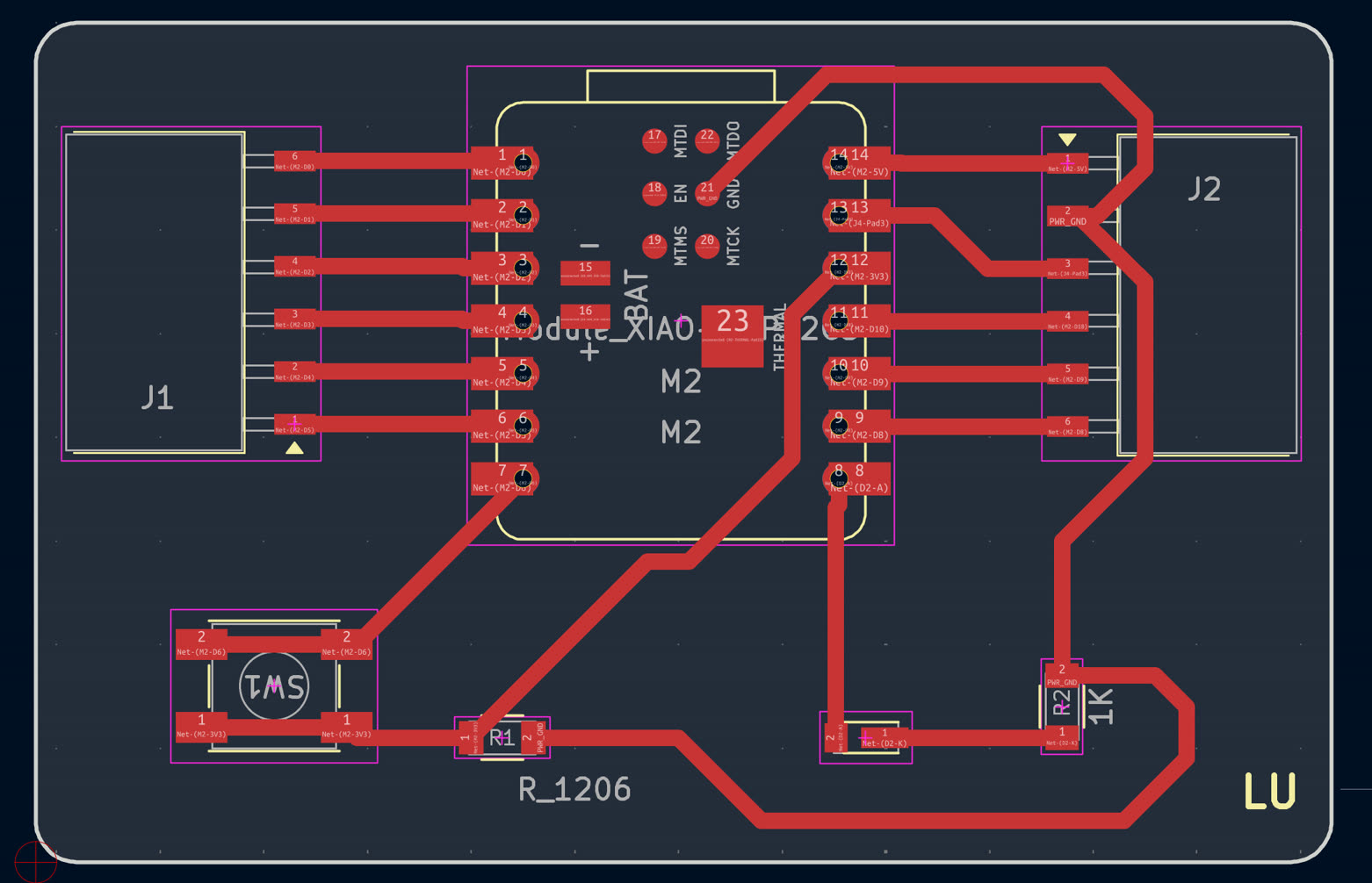
8. PCB design
After the ERC check with no errors, I initiated the transition from schematic to physical layout by using the Update PCB from Schematic tool, successfully importing the netlist and footprints into the PCB Editor.
I put all the parts on the sheet.
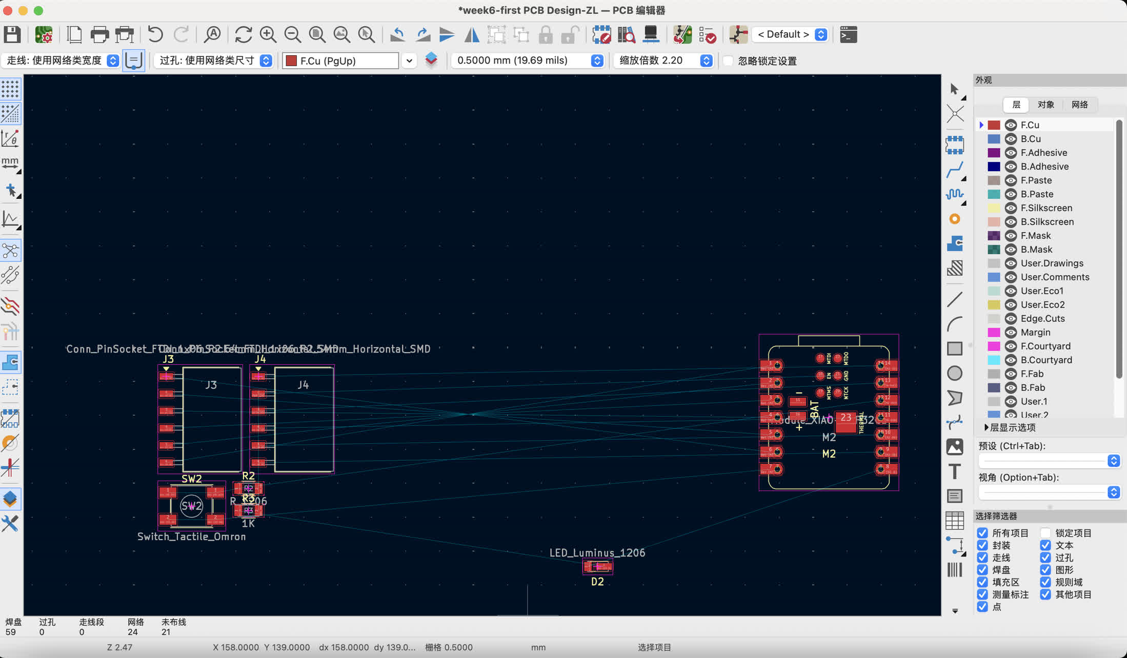
To ensure the board could be reliably manufactured using a CNC milling machine, I configured the Board Setup.
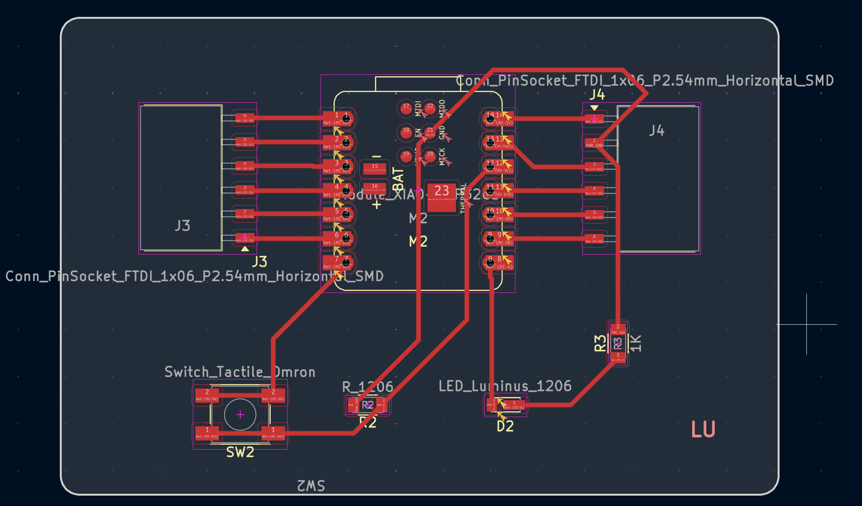
During the Component Placement phase, I aligned the two pin sockets to match the XIAO ESP32C3 footprint and strategically positioned the LED, resistor, and button to minimize crossing "ratsnest" lines.
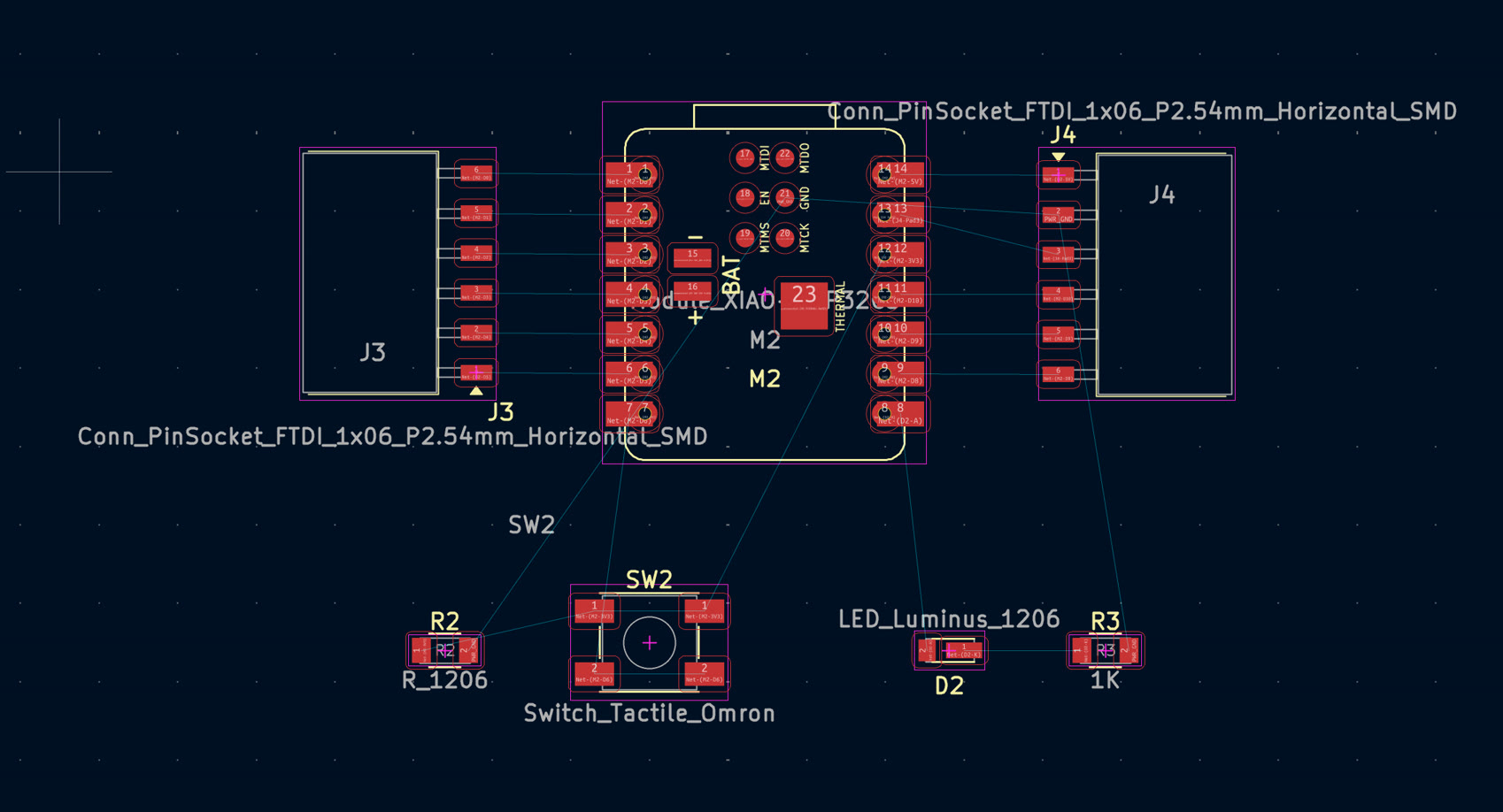
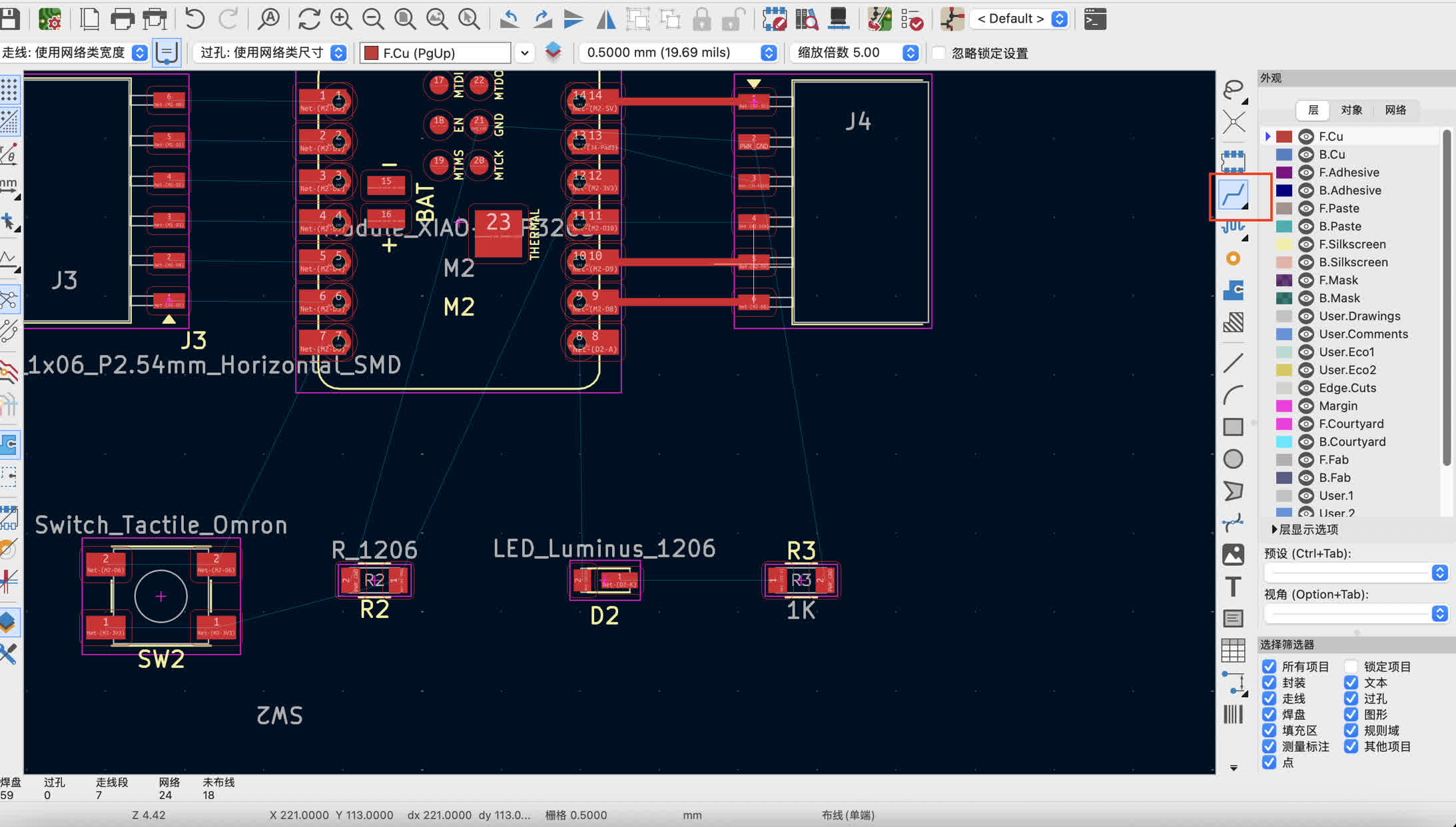
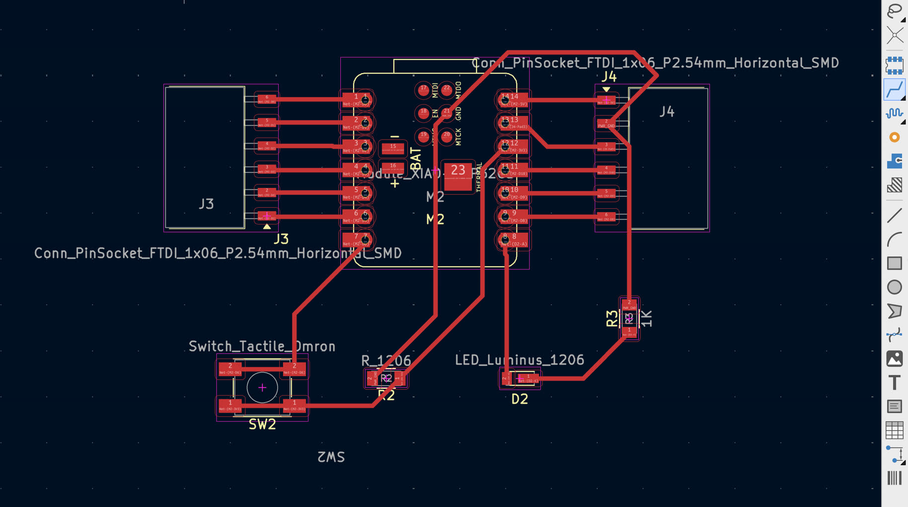
I performed Manual Routing by using the Route Tracks tool, adhering to professional standards by using 45-degree angles for all copper traces to ensure signal integrity and aesthetic clarity.
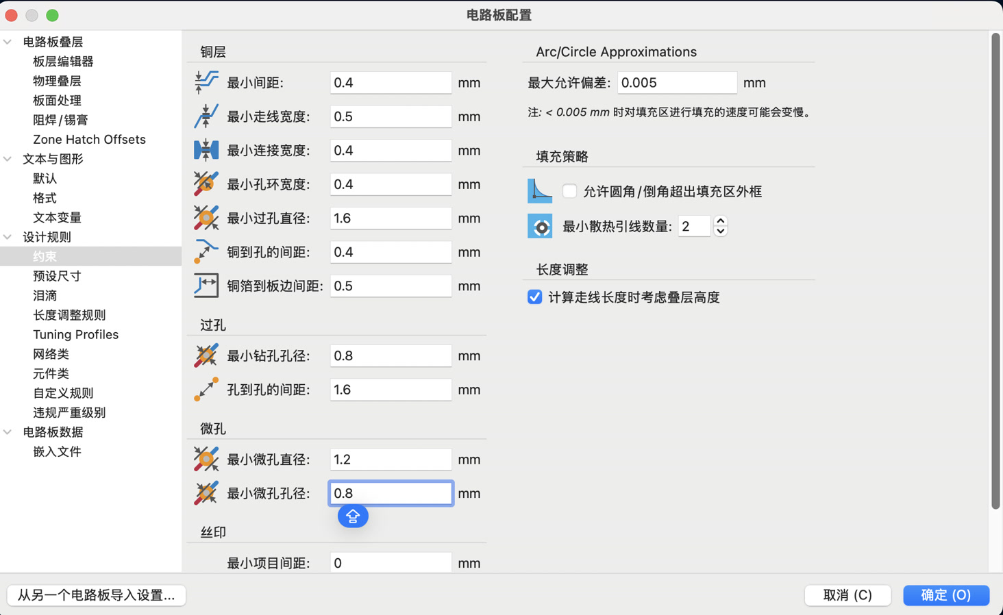
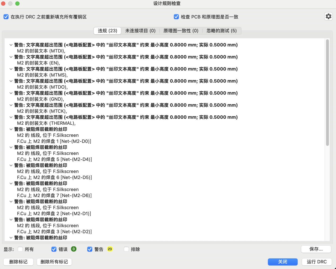
Once routing was complete, I ran the Design Rule Check (DRC) to verify that there were zero unconnected nets and that all clearances met the specified manufacturing constraints. I encountered errors and warnings.
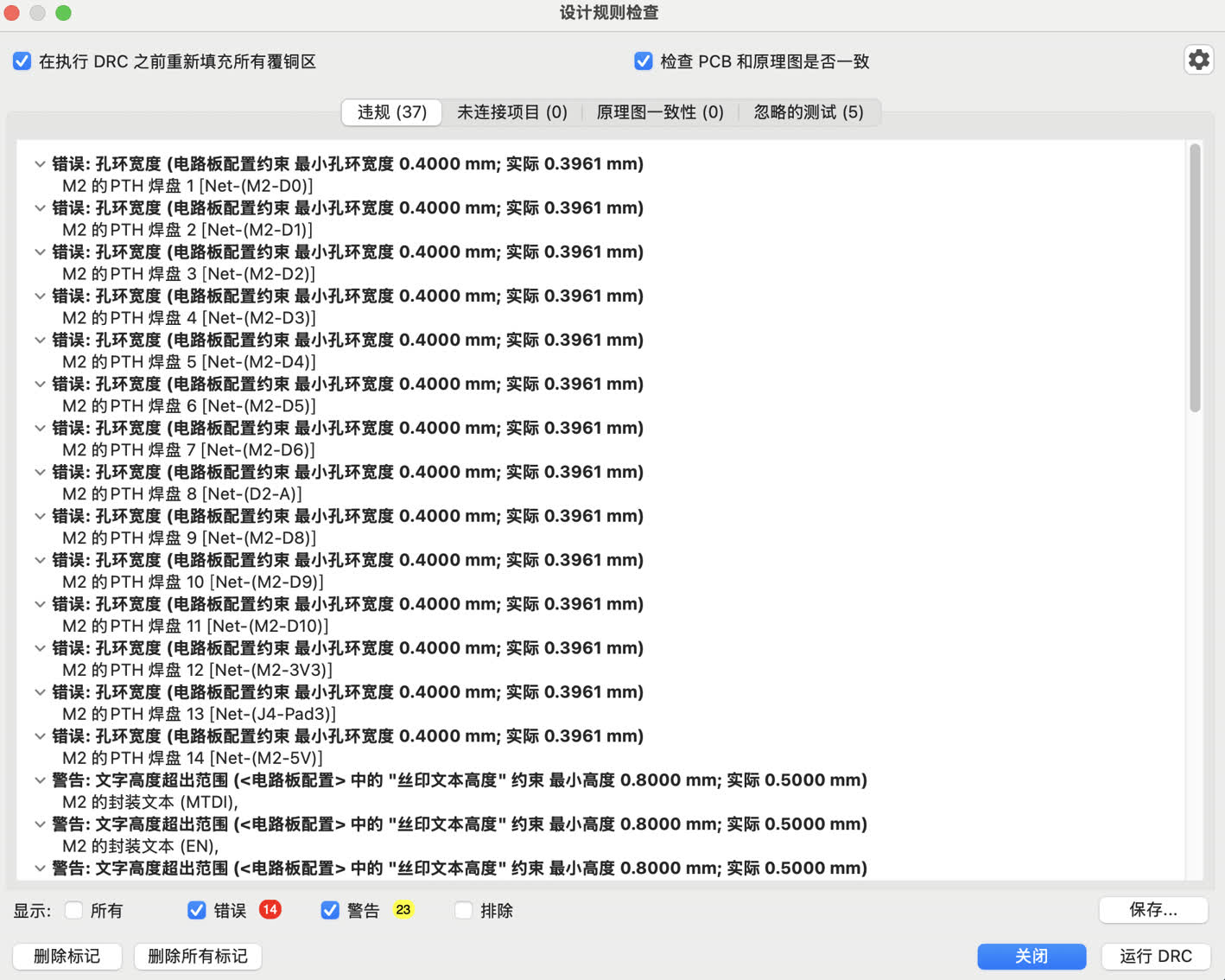
I changed the setting of minimum hole ring width to fix it.
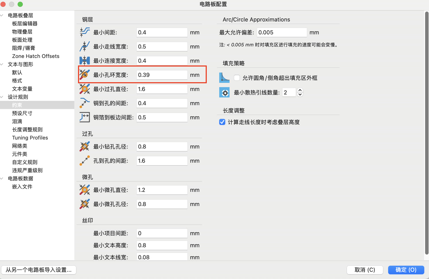
Run DRC again, now I still have some warnings.
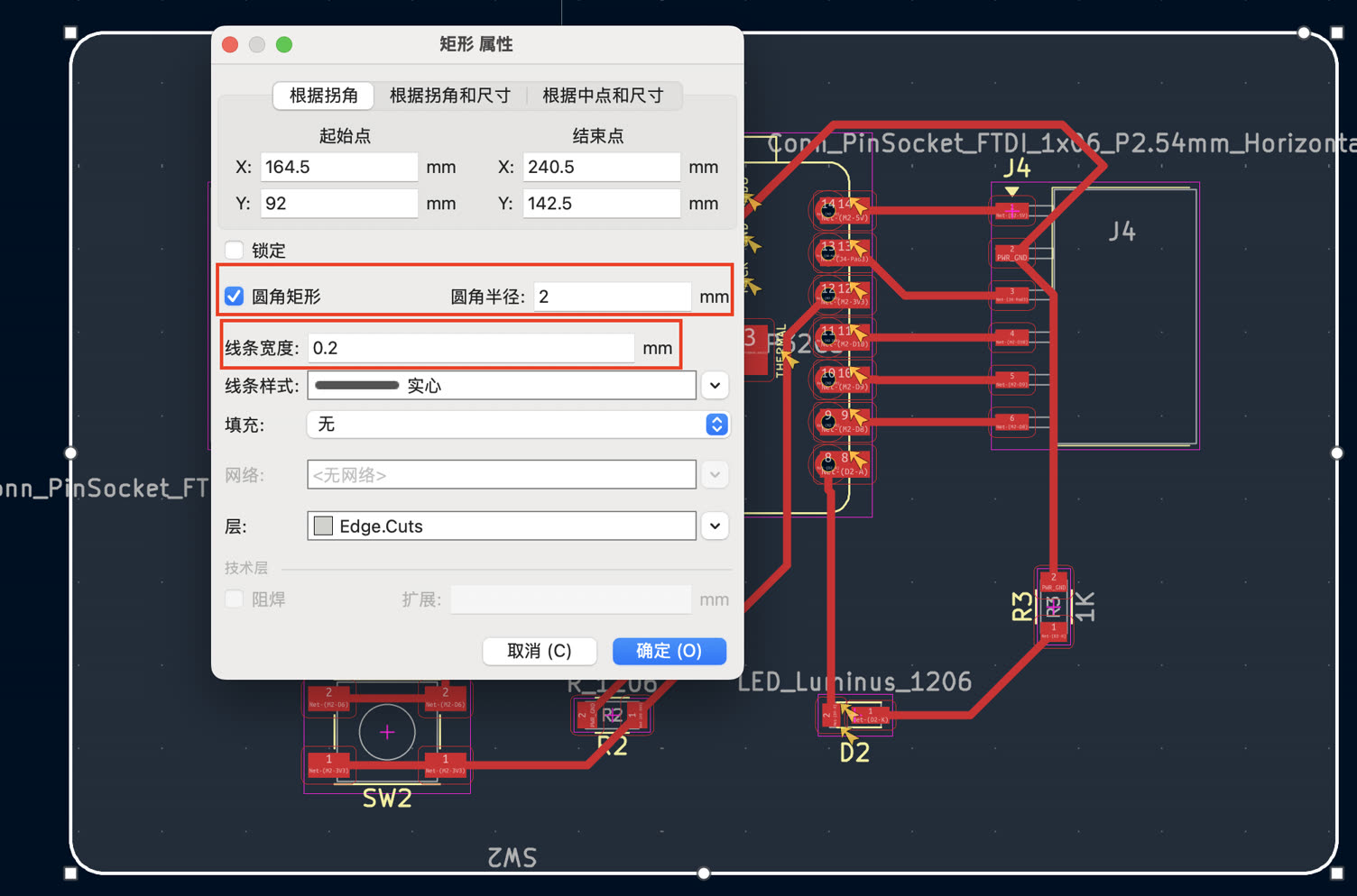
I defined the physical boundary of the board by switching to the Edge.Cuts layer and drawing a closed rectangular perimeter with 2mm rounded corners, providing a safe margin around the components.
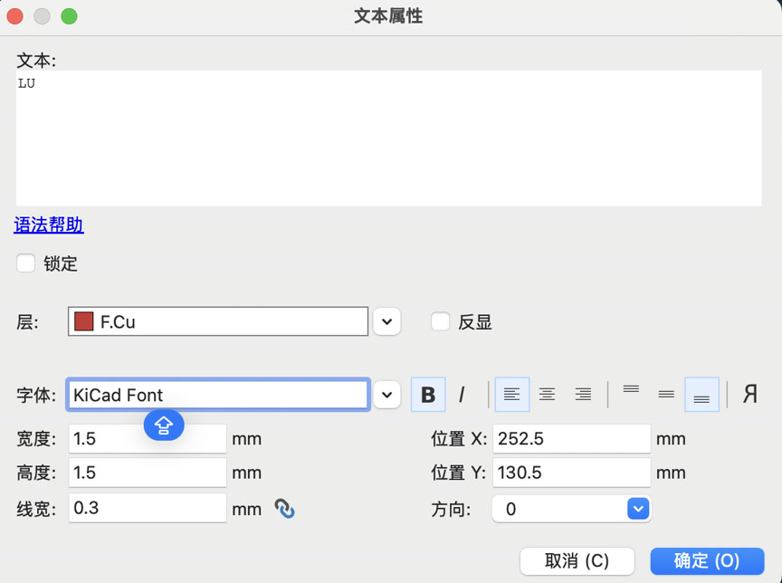
For personalization and identification, I added my name "LU" to the F.Cu (Front Copper) layer using the text tool, ensuring the identifier would be physically milled onto the board.
Then I am close to finalize the design of PCB.
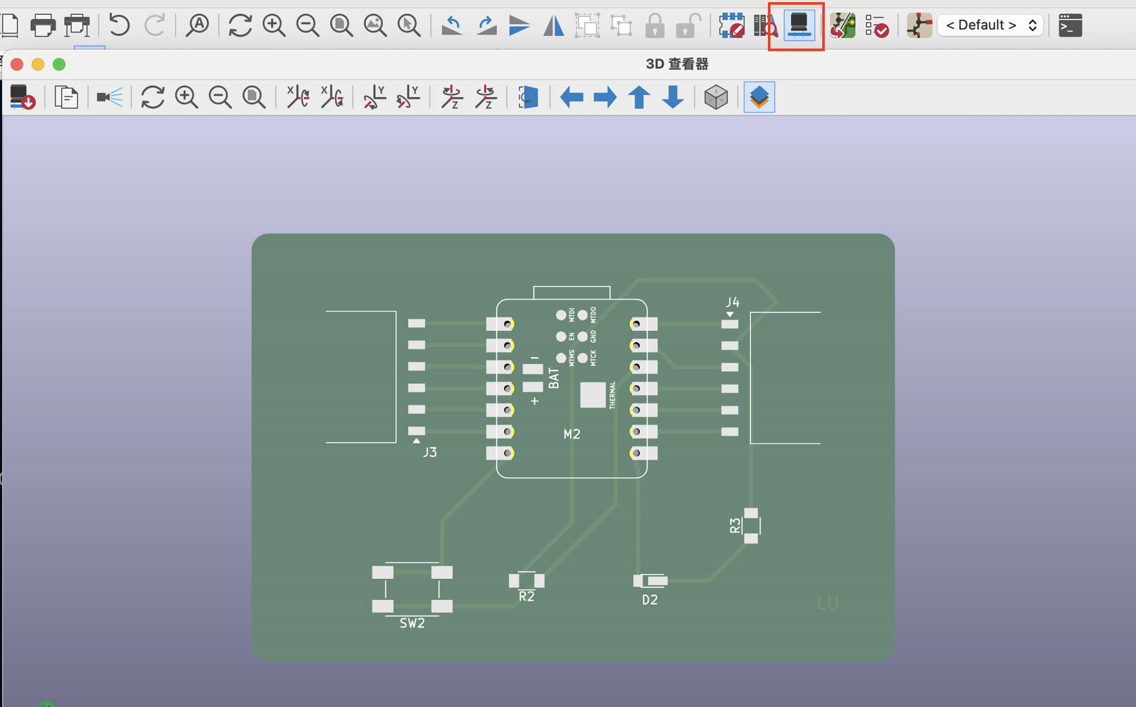
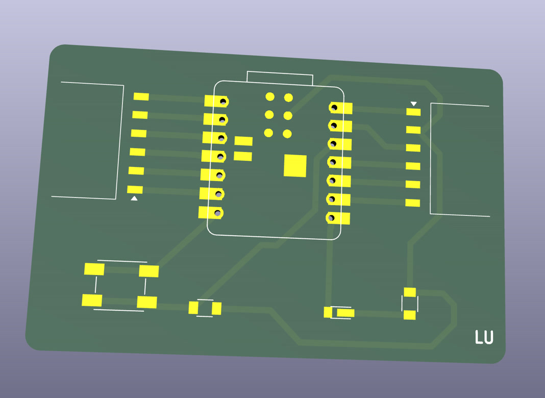
Finally, I utilized the 3D Viewer to perform a comprehensive visual inspection, confirming that the board geometry was correct and that all components were properly oriented before exporting the fabrication files.
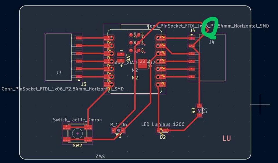
I just found a right angle routing here, and I fixed it.
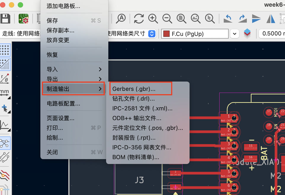
Then I exported my design to Gerber file. I utilized the Fabrication Outputs > Gerber tool to generate the industry-standard files for my design. I plotted the F.Cu (Front Copper) and Edge.Cuts layers, ensuring the mechanical dimensions and electrical traces were accurately captured for the PCB manufacturing process.
Update 0419:
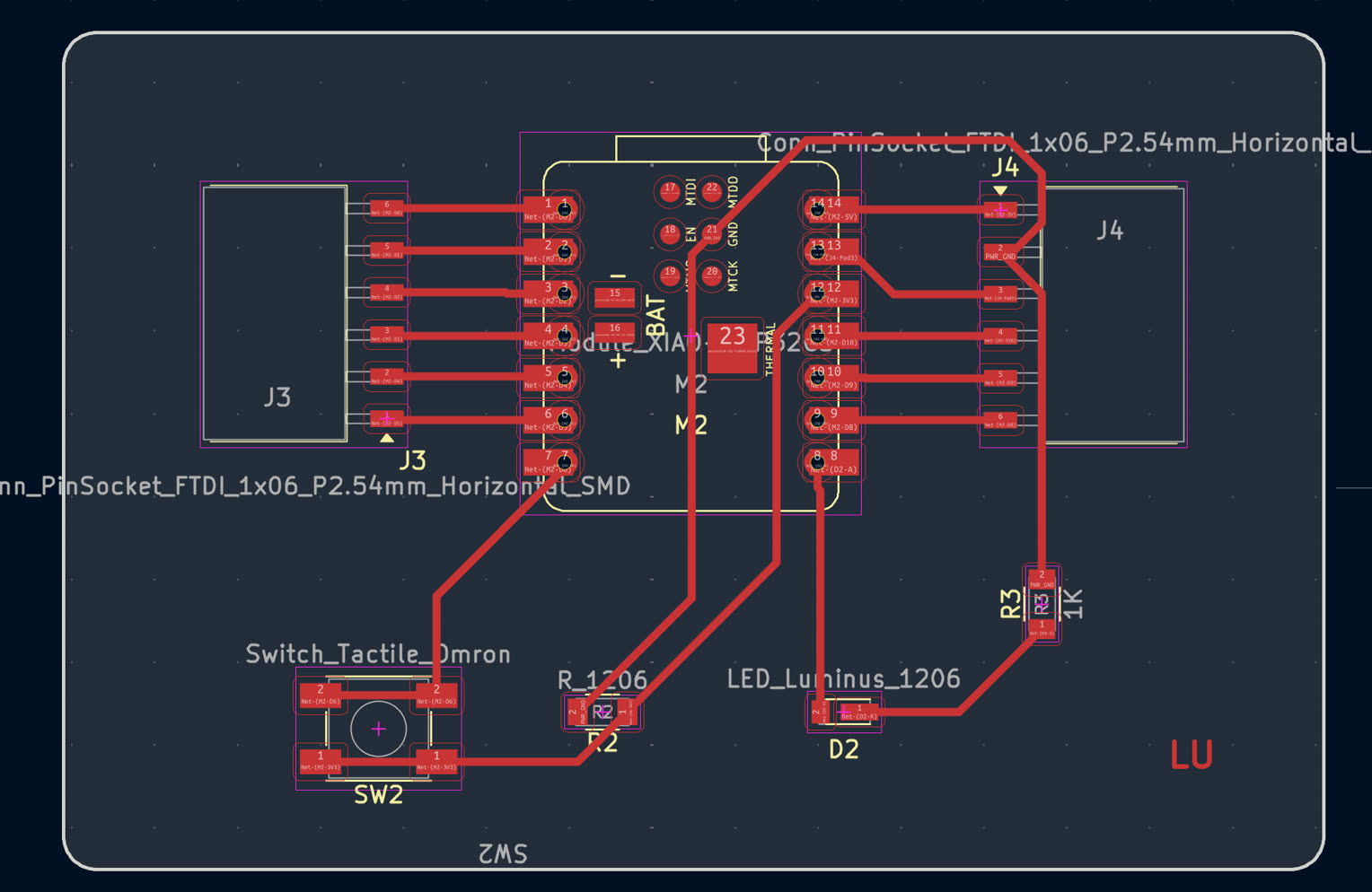
During Week 8 (electronics production), I encountered a problem during in-house copper-clad board cutting production. Since the width of the trace is 0.5mm, some copper lines are separated from the board, or even broken.
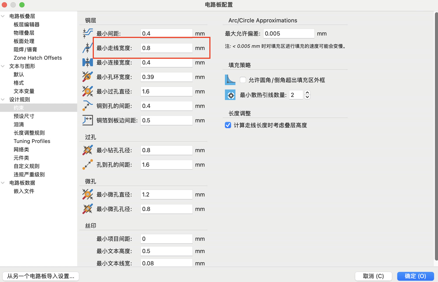
I tried to revise the setting of the width to 0.8mm, and then realized it can only be settled before drawing the wiring of PCB design.
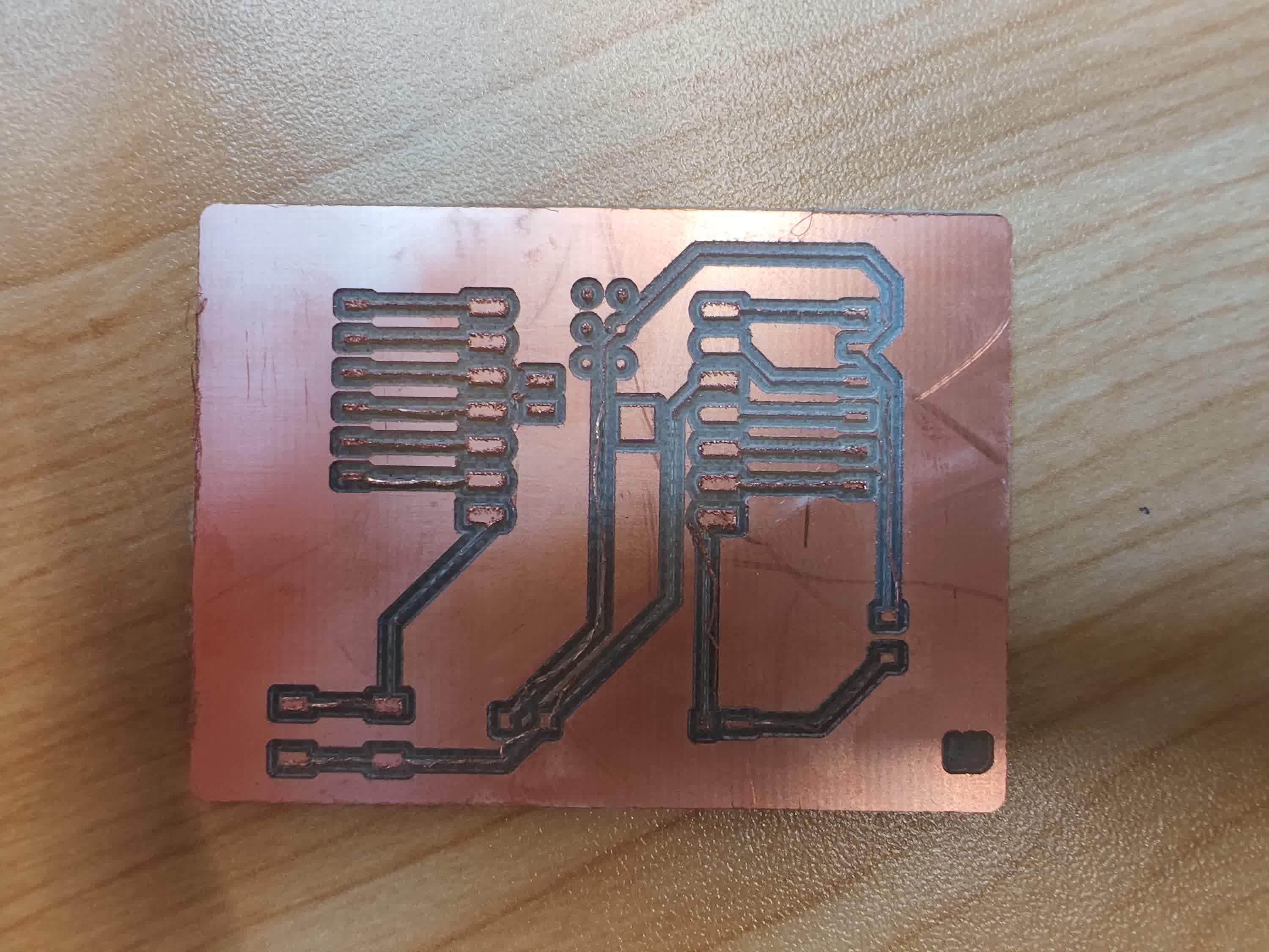
After confirming this problem, I settled the width of the trace to 0.8mm, and drew the wiring again.
The updated Gerber files:
week6-first PCB Design-ZL-Edge_Cuts.gbr week6-first PCB Design-ZL-F_Cu.gbr