Week 8 — Group Assignment: Electronics Production
Characterise how we make PCBs at Chaihuo — both in-house and through a board house:
- Characterize the design rules for our in-house PCB production process and document the machine settings
- Document the workflow for sending a PCB design to a board house
- Document the work on this group page; each student reflects on what they learned when completing the individual assignment (make and test an embedded system you designed)
See assignment requirements for the full brief.
This page documents our Week 8 group collaboration at Chaihuo Makerspace: milling PCBs on the lab KEXU CNC, finding working parameters, and ordering the same design from JLCPCB. PCB layouts came from the Week 6 electronics-design work.
In-House PCB Milling
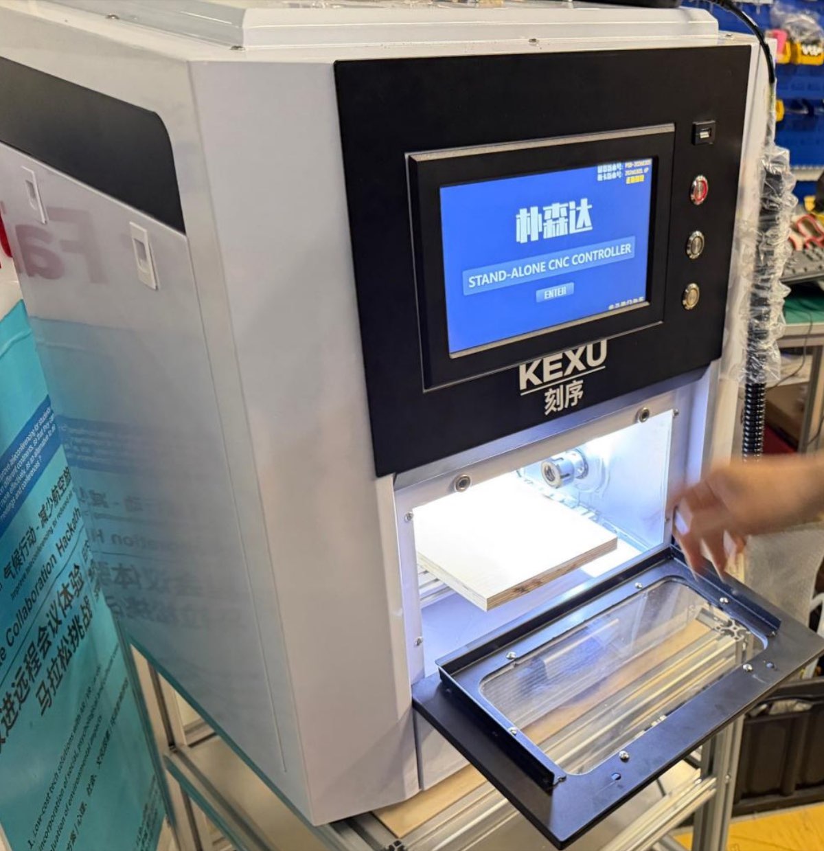
Machine — KEXU (Exu Turbo)
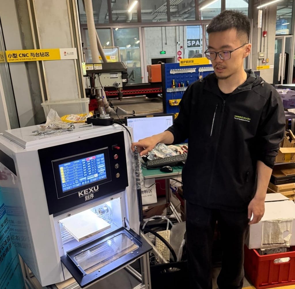
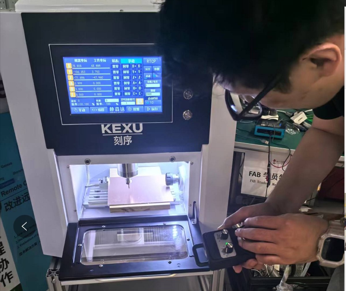
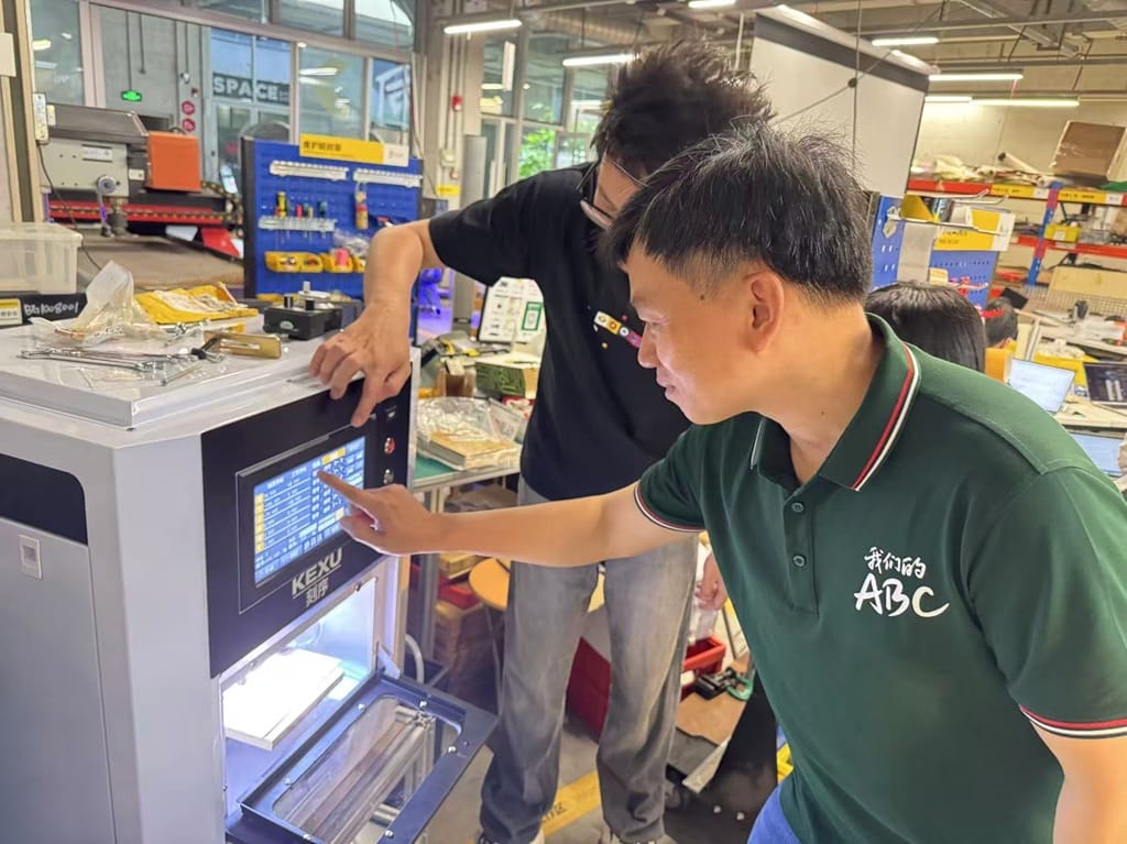
Our in-house PCB production uses the KEXU desktop CNC at the Small CNC & Drill Press area. Instructor Matthew walked the group through safety and setup before the first cut.
| Specification | Details |
|---|---|
| Model | Exu Turbo (3-axis) |
| Overall dimensions (L × W × H) | 550 × 490 × 620 mm |
| Travel (X / Y / Z) | 190 × 120 × 110 mm |
| Relief carving area | 200 × 120 mm |
| Spindle speed | 0 – 24,000 rpm |
| Spindle power | 800 W, water-cooled |
| Machining speed | 0 – 4000 mm/min |
| Tool holder capacity | 1 – 6 mm |
| Control | 7-inch touch screen (Wi-Fi / USB) |
Safety: wear a mask and safety goggles when milling FR-4 — the dust is fine and should not be inhaled.
Material and tools
| Item | Specification |
|---|---|
| Substrate | FR-4 epoxy glass fibre (single-sided copper) |
| Board thickness | 1.5 – 1.6 mm |
| Copper thickness | 35 μm (1 oz) |
| Trace bit | 40° #502 V-bit |
| Outline bit | 4-flute end mill (~1.5 mm) |
Design rules and machine settings
We tested different feed/speed/depth combinations until traces were clean and outlines cut through without snapping the bit. These are the parameters we settled on:
| Parameter | V-bit (tracing) | Ball-end / end mill (outline) |
|---|---|---|
| Feed speed | 4 mm/s | 4 mm/s |
| Spindle speed | 14,000 rpm | 14,000 rpm |
| Offset number | 4 | 4 |
| Offset stepover | 0.2 mm | 0.2 mm |
| Cut depth | 0.23 mm | 0.45 mm |
| Tool diameter (effective) | 0.3 mm | 1.5 mm |
The 0.23 mm trace depth removes copper without cutting too deep into the substrate. The 0.45 mm outline depth per pass cuts through the board in several passes without overloading the bit.
Practical design limits for in-house milling:
| Rule | Value / note |
|---|---|
| Minimum reliable trace/space | ~0.38 mm |
| Trace width recommendation | 1 mm for power buses; 0.5 mm signal traces can be fragile after milling |
| Isolation routing | Multiple offset passes (4 × 0.2 mm stepover) |
| Board fixturing | Double-sided tape on sacrificial layer; board must stay flat |
| Z zero | Lower bit until it just touches copper (paper / tape drag test), then set Z = 0 |
| File transfer | FAT32 USB; avoid hyphens in filenames — the controller rejects them |
Milling workflow
The full in-house workflow at Chaihuo:
- Design in KiCad (schematic + PCB from Week 6)
- Export Gerber — at minimum
F_Cu.gbr(traces) andEdge_Cuts.gbr(outline) for milling - Convert to PNG — use gerber2png or KiCad plot
- Generate G-code in Mods — upload PNG on the Mods CE, select 40° V-bit for traces and end mill for outline, simulate, save
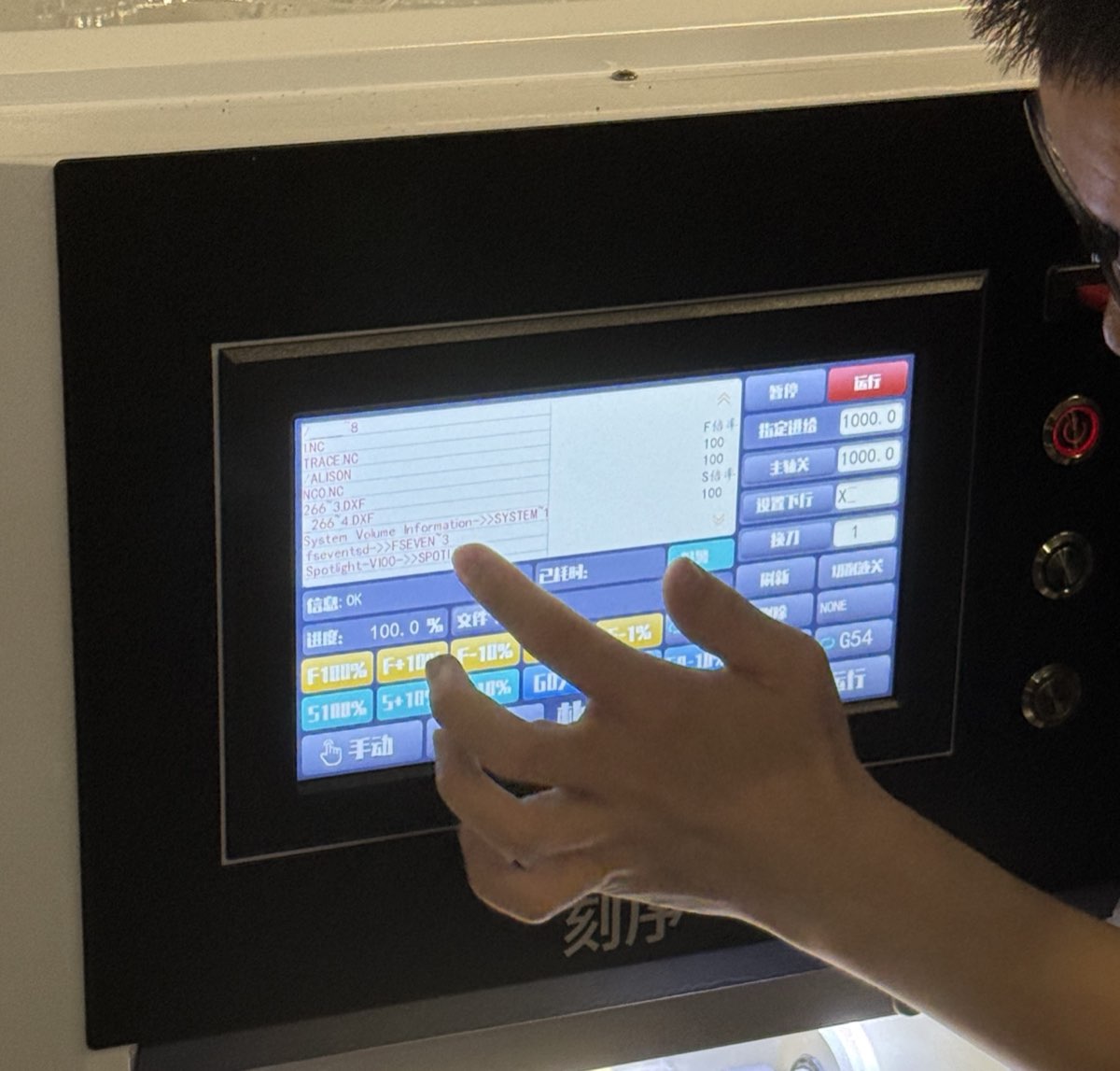
.nc - Load on machine — copy
.ncfiles to USB, select trace file first then outline - Zero and run — set X/Y at board corner, Z on copper surface; start with conservative depth and adjust if the first pass looks shallow
- Deburr and clean — scrape loose copper with a steel ruler; wash with soap and water to remove oils
Use Chrome or Edge with Mods. Some browsers (e.g. Brave) produce bad toolpaths — unwanted dots or irregular patterns.
Machine setup (photos)
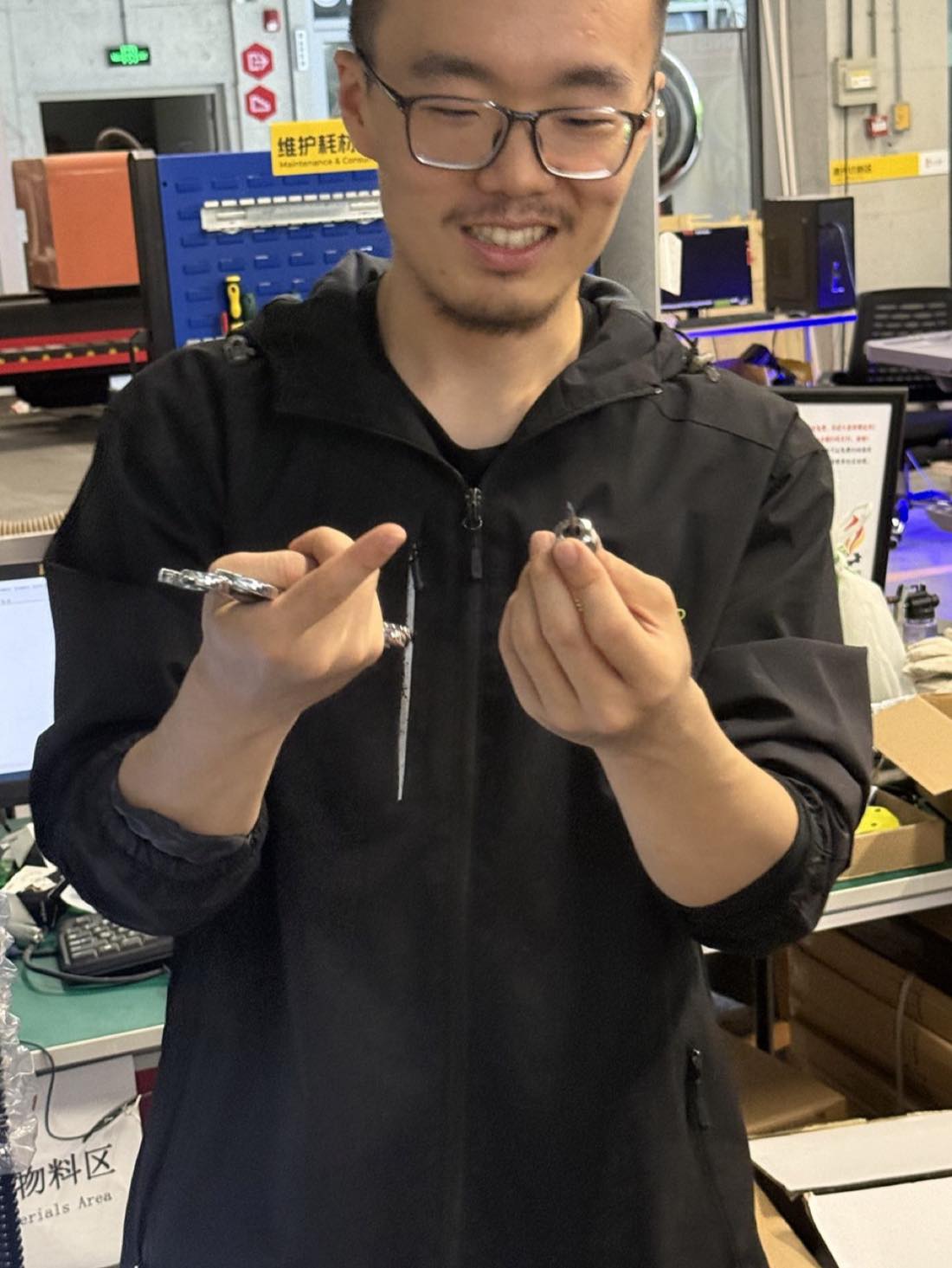
Install the V-bit in the collet and tighten with the wrenches provided.
 |  |
|---|
Secure the copper-clad board on the sacrificial layer with tape or a toe clamp. Jog the spindle to the front-left corner for X/Y zero.
 |  |
|---|
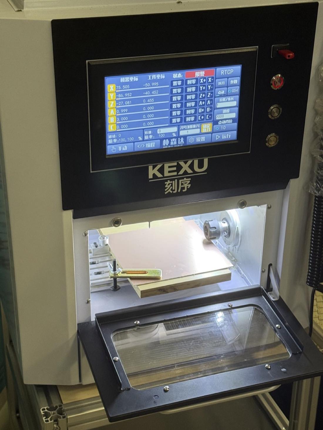
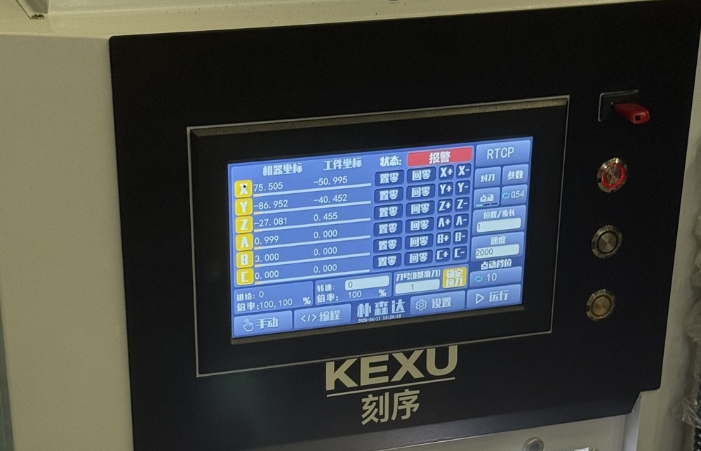
Set X, Y, Z zero on the touch-screen controller:
| Axis | Method |
|---|---|
| X, Y | Move tool to front-left corner of copper board → Set XY Zero |
| Z | Lower until bit touches copper (paper drag test) → Set Z Zero |
 |  |
|---|
Select the G-code file from USB (TRACE.NC, outline file) and run. Pause and re-zero Z if the first pass is too shallow or too deep.
Laser cutting (explored, not recommended)
We also tested LaserPecker 3 (diode laser) for copper removal. With negative SVG plots from KiCad (white = keep traces, black = remove copper), a single pass took ~10 minutes but did not fully isolate the traces even after multiple passes. A fibre laser can remove copper in fewer passes; our diode laser is useful for marking but not reliable as a primary PCB fabrication method. Vinyl cutting was explored separately by other students — see Emily's documentation linked from Timothy's Week 8 page.
Submitting a PCB to a Board House
In-house milling is fast for prototyping (roughly one hour per board) but limited to ~0.38 mm features and produces boards without solder mask or silkscreen. When we need cleaner boards, tighter spacing (~0.125 mm), or more than a handful of copies, we send the design to a board house.
Files needed
Milling only needs two Gerber layers. A board house needs the full fabrication package:
| File | Purpose |
|---|---|
F_Cu.gbr | Front copper traces |
Edge_Cuts.gbr | Board outline |
F_Mask.gbr | Front solder mask (exposes pads only) |
B_Mask.gbr | Back solder mask (often includes drill info) |
F_Silkscreen.gbr | Component labels and polarity marks |
.drl (or embedded in mask) | Drill locations, sizes, plated vs non-plated |
Solder mask is the coloured polymer coating that protects copper and prevents solder bridges. Silkscreen prints reference designators (R1, C2, …) on the surface for assembly. Both are generated from the same KiCad design used in Week 6 — export via File → Fabrication Outputs → Gerbers.
Ordering at JLCPCB
Instructor Matthew introduced JLCPCB (JLC Technology Group, Shenzhen) as a fast, low-cost option for our cohort. Workflow:
- Export and zip all Gerber + drill files from KiCad
- Upload the zip to jlcpcb.com
- Review auto-detected parameters — board size, layer count, thickness; adjust if needed
- Confirm the preview — side-by-side design vs production draft plus 3D view; last chance to catch layer errors
- Pay and wait — production typically starts within a day; delivery to Shenzhen is 2–7 days depending on courier
Typical order settings for our development boards:
| Parameter | Value |
|---|---|
| Board material | FR-4 |
| Layer count | 2 |
| Board thickness | 1.0 – 1.6 mm |
| Surface finish | Lead-free HASL |
| Electrical test | Flying probe (free) |
| Quantity | 5 boards |
Our group orders came to roughly ¥40 RMB (~$6 USD) for 5 boards plus shipping. One order placed 23 March arrived 25 March; another cohort order (via JLCPCB from Timothy's test) cost $5.56 for 5 boards with shipping to Shenzhen — delivery took 7 days because the courier required an answered phone call before drop-off.
Milled vs board-house boards
| In-house (KEXU) | Board house (JLCPCB) | |
|---|---|---|
| Turnaround | ~1 hour | 2–7 days |
| Trace quality | Good for ≥0.38 mm; edges rougher | Clean, consistent |
| Solder mask | None | Green (or other colour) |
| Silkscreen | None | Reference designators printed |
| Best for | Rapid iteration, debugging | Cleaner assembly, final-ish prototypes |
Both methods have a place: mill first to validate the design, then order from JLC when the layout is stable.
What We Learned
- Measure and zero carefully. A board that is not flat or a Z zero that is slightly off produces shallow traces or cuts into the sacrificial layer.
- In-house rules are tighter than board-house rules. Design for ≥0.38 mm traces/spacing when milling; use wider buses where possible.
- Mods + a post-processor bridge the gap between MIT's toolchain and our KEXU controller — always simulate in Mods and test-cut before committing copper.
- Board-house export is a different mindset. Solder mask, silkscreen, and drill files each serve a fabrication step you do not think about when milling.
- Check the JLC preview. The 3D render catches mirrored layers and missing drill files before they become expensive mistakes.
- Clean the milled board before soldering — remove tape residue and wash off FR-4 dust.
These group findings feed directly into each student's individual assignment: populate and test the embedded system on either a milled or ordered board.