Week 8 : Electronics Production
Week 8 assignment could be categorized as follows:
-
Group assignment
- Design rules characterisation (in-house PCB)
- PCB milling
- Laser cutting
- PCB design submission to a board house
- Design rules characterisation (in-house PCB)
-
Individual assignment
- Fabrication and testing (designed embedded microcontroller system)
For basics of PCB design, please refer to Week 6 : Electronics design
Basics of PCB fabrication
-
Methods for PCB fabrication:
- Chemical: etching, lithography, toner transfer, printing
- Mechanical (more common for rapid prototyping):
- PCB milling
- Bit types:
- V: Sharp V-shaped tip with straight sides forming an angle. The cutting width depends on the depth the tool cuts into the board—deeper cuts produce wider traces. V-bits are useful for fine traces but can create more vibration.
- Tapered: A tapered bit has a gradually narrowing body with a small flat or rounded tip. Tapered bits vibrate less and last longer, making them better for consistent milling and deeper cuts.
- Bit types:
- Laser cutting: See week 3 for more details
- PCB milling
-
PCB materials:
- FR4 (epoxy glass): Usually used by board houses. Hazardous, fire resistant up to NEMA4.
- FR1
- Garolite
-
Zeroing: The distance between the tip of the bit and the surface of the PCB. When the bit just touches the board surface, that position is set as Z = 0.
- Mounting: Attaching the PCB firmly to work surface - using clamps, double-sided tape, vacuum table, etc.) to ensure surface of the material is even and does not move during milling due to vibration
- Lowering: Moving the milling bit downward toward the PCB surface until it reaches the correct height for zeroing or cutting. During setup, the operator slowly lowers the bit until it just touches the surface of the board, which is then used to set the Z-axis zero point.
Design rules characterisation
PCBs are generally better than breadboards due to the following reasons :
- Breadboards require through-hole components and therefore a separate inventory is needed for it
- Contacts in breadboards are not very mechanically reliable, which can introduce parasitic resistance and capacitance
Mechanical methods namely PCB milling, laser cutting and vinyl cutting methods were explored. For the latter, please refer to Emily's documentation
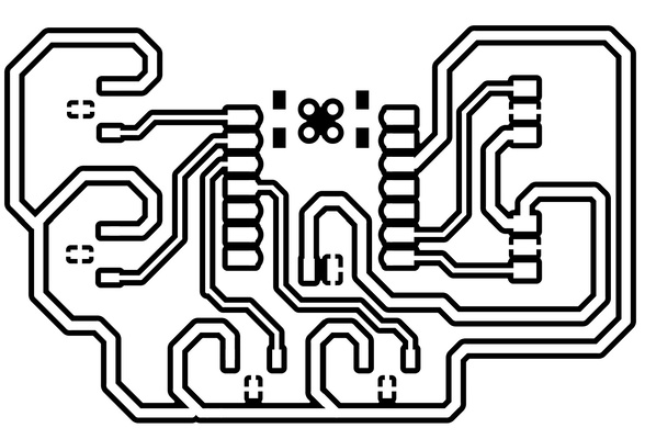
The PCB design used in these experiments are based on the layouts developed in Week 6 : Electronics design.
PCB milling
PCB CNC milling Safety
Appropriate mask and safety goggles are recommended to prevent exposure to airborne FR-4 dust.
The following tools and materials were used to fabricate the PCB with the CNC.
- Working machining envelope/area : 190 mm (X) × 120 mm (Y) × 110 mm (Z)
- Spindle speed : 0 to 24,000 RPM
- Clampable tool diameter : 1 mm to 6 mm
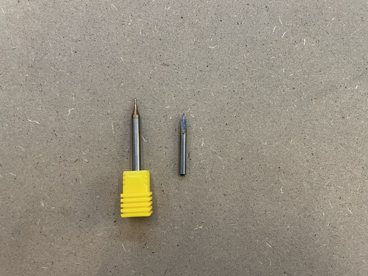
- 4-flute end mill (for edge-cutting). Since the scale of fabrication is less than CNC wood milling, chip load is less of a concern.
- 40° V-bit (for traces)
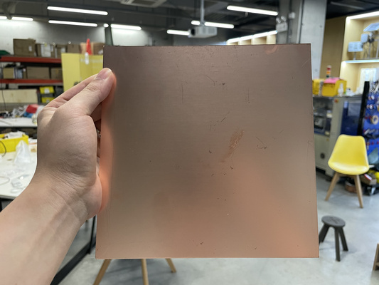
- Substrate : FR4
- Sides : Single-sided. Copper is present on only one side of the board
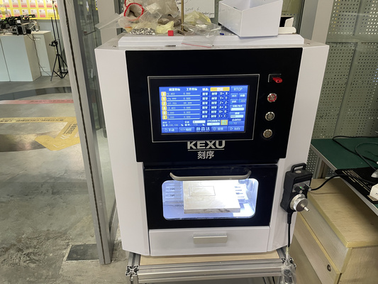
- Board thickness : 1.5 mm Additional details on the CNC machine could be found at Chaihuo's 2026 Week 8 group assignment.
The milling process is divided into three steps :
- G-code creation with Mods
- G-code conversion for CNC milling machine compatibility
- CNC execution (e.g. zeroing)
G-code creation with Mods
The PCB CNC milling process is divided into several steps with the mods module serving as the central tool that works either with PNG or SVG. Below are the steps based on the former and the CNC machine described above:
- Top copper layer and edge cut Gerber files export (e.g. from KiCAD)
- Convert gerber files to PNG using the gerber2png
- Click "open in Mods" or open Mods manually, then upload PNG.
- Select the appropriate bits. In this case 40° V bit for traces and end mill for the edge cuts
- Click calculate. Simulate and check toolpath.
- Save G-code file
Browser compatibility with Mods
Compatibility issue might occur between certain browsers with Mods. Browser like brave can lead to unexpected toolpaths such as unwanted dots or irregular patterns.
Therefore it is recommended to use standard ones such as Edge or Chrome.
Deburring (removing small copper or board fragments left from milling) can be performed using a steel ruler. Washing with soap and water also removes oils from handling and residues
G-code conversion for CNC milling machine compatibility
This process is used to ensure compatibility of G-code for the abovementioned CNC milling machine. A python code that introduces commands of 5 mm clearance height at the start and end of the program, forces spindle speed of 11000 RPM, etc, is created based on successful output test from the ArtForm X64 software.
The python code could be seen at the admonition below.
GPS x XIAO ESP32C3 code
#!/usr/bin/env python3
from pathlib import Path
import re
import sys

STARTUP_PATTERNS = [
    r'^G17$', r'^G21$', r'^G40$', r'^G49$', r'^G54$', r'^G80$', r'^G90$', r'^G94$',
    r'^G98$', r'^F[-+]?\d', r'^S[-+]?\d', r'^M0?3$', r'^G0?0Z'
]

def convert_file(src_path: Path, program_number: int) -> Path:
    lines = src_path.read_text(errors='replace').splitlines()
    clean = [ln.strip() for ln in lines if ln.strip() and ln.strip() != '%']

    body = []
    started = False
    for ln in clean:
        if not started and any(re.match(p, ln, re.I) for p in STARTUP_PATTERNS):
            continue
        started = True
        body.append(ln)

    while body and re.match(r'^(M0?5|M30|%)$', body[-1], re.I):
        body.pop()
    while body and re.match(r'^G0?0X0+\.?0*Y0+\.?0*(Z20(?:\.0*)?)?$', body[-1], re.I):
        body.pop()
    while body and re.match(r'^G0?0Z(2|5|20)(?:\.0*)?$', body[-1], re.I):
        body.pop()

    adapted = [
        '%',
        f'O{program_number:04d}',
        '(ADAPTED FOR FAB2026-STYLE CNC STARTUP)',
        'G90 G40 G49 G80 G94',
        'G21 G17 G54',
        'T1 M6',
        'S11000 M03',
        'G00 G90 X0.0000 Y0.0000 M08',
        'G43 Z5.0000 H1',
        'Z2.0000',
    ]
    adapted += body
    adapted += [
        'G00 Z5.0000',
        'G00 X0.0000 Y0.0000',
        'M09',
        'M05',
        'M30',
        '%'
    ]

    out_path = src_path.with_name(src_path.stem + '_chaihuo_compatible.nc')
    out_path.write_text('\n'.join(adapted) + '\n', encoding='utf-8')
    return out_path

def main():
    if len(sys.argv) < 2:
        print('Drag one or more .nc files onto this script, or run:')
        print('python gcode_drag_drop_converter.py file1.nc file2.nc')
        input('\nPress Enter to close...')
        return

    converted = []
    skipped = []

    for idx, arg in enumerate(sys.argv[1:], start=2):
        src = Path(arg)
        if not src.exists() or src.is_dir():
            skipped.append((arg, 'not a file'))
            continue
        if src.suffix.lower() != '.nc':
            skipped.append((arg, 'not an .nc file'))
            continue
        try:
            out = convert_file(src, idx)
            converted.append((src, out))
        except Exception as e:
            skipped.append((arg, f'error: {e}'))

    print('\nConversion finished.\n')
    for src, out in converted:
        print(f'OK: {src.name} -> {out.name}')

    if skipped:
        print('\nSkipped:')
        for name, reason in skipped:
            print(f'- {name}: {reason}')

    print('\nImportant machine checks before running:')
    print('- Confirm T1 and H1 match your actual tool and tool-length offset')
    print('- Remove M08/M09 if your CNC does not use coolant')
    print('- Confirm G54 zero is correct for the job')
    input('\nPress Enter to close...')

if __name__ == '__main__':
    main()
This particular CNC milling machine cannot read file names with hyphens (-)
CNC execution
The G-code could then be moved to the CNC machine using the FAT32 type USB (see Week 7 : Computer-controlled machining for more details). Before starting the cutting process, it is important to ensure the following :
-
Ensure that the double-sided tape is pressed firmly against the sacrifical layer to ensure it is completely flat. This prevents uneven surfaces that would otherwise cause Z-zero reference to vary across the board. Only minimal copper dust or fine powder should be produced if calibration is done properly.
-
The zeroing could be done by lowering the Z-axis slowly until the milling bit just makes contact with a layer of a tape and it no longer shifts. This position is then set to Z-zero. The Z-axis then could slightly shifted up and the return function could then move the tool back to the Z-zero positoin.
For the edge cut, it may be necessary to slightly adjust the Z-zero position as the default setting in Mods is typically 1.7018 mm of maximum depth. This value may need to be tuned depending on the material thickness and machine calibration to ensure a clean cut without excessive penetration into the sacrificial layer.
Safe Z-height setup and test cutting workflow
Start with an initial Z height. Run the CNC milling job for the first pass and observe how the tool engages with the material.
If the cut does not look correct:
- Pause the job immediately
- Use the machine’s return-to-origin / reset-to-zero feature to bring the tool back to the starting reference point
- Carefully adjust the Z-axis (Z-zero or depth offset) as needed
- Then restart the operation
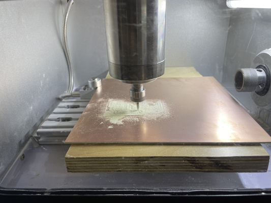
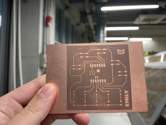
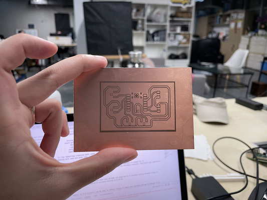
Select the file of interest and then let the milling begin. The result of these settings could be seen below and the whole process lasts roughly 1 hour, and also wash with soap so that it's clean:
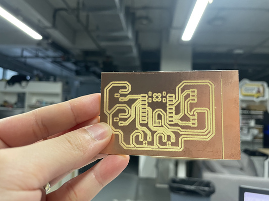
Result and observation : In future iterations it might be beneficial to switch to a 1 mm traces thickness for all of the buses (original design was using 1 mm for power bus, while signal buses were 0.5 mm). This adjustment would perhaps reduces the possibility of milled traces being overly thin or fragile.
Laser cutting
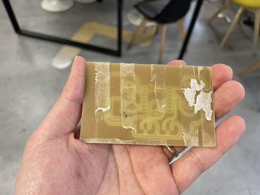
The LaserPecker 3 (diode laser) was used; however, it was unable to fully remove the copper layer or would have required a very long time (hours). Chemical etching or other methods may be needed to assist the process, but this is not further explored
Here are some details about the LaserPecker 3 machine based on the official website:
- Laser type : Diode
- Laser wavelength : 1 μm
- Laser spot size : 0.01 mm (the smaller it is, the finer the details could be)
Laser Safety
- The LaserPecker 3 uses a 1 μm infrared laser, which can cause eye injury even if the beam is not visible. Always wear appropriate laser safety glasses rated for 1 μm.
- Operate the device in a well-ventilated area, as engraving metals or plastics can produce harmful fumes.
- Do not leave the laser unattended while it is powered on.
- Maintain a safe distance of at least 50 cm from the laser during operation.
Source: ChatGPT by OpenAI, March 2026
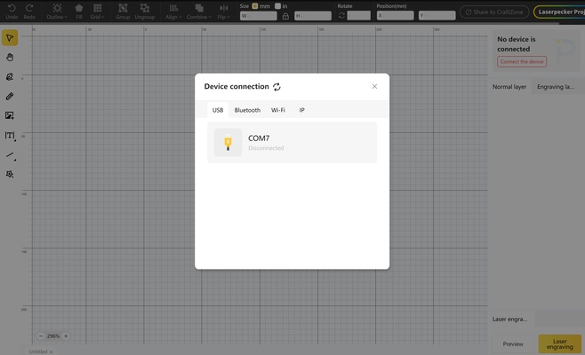
The LaserPecker 3 comes with a mobile app and can theoretically connect via Bluetooth. However, during the test it didn't seem to work and so the alternative - the laptop software called Laser Pecker Design (LSD) Spaceand connection via USB to the machine - was used and the following documentation focuses on that.
The design must be exported as an SVG file. The laser interprets black areas as material to be removed, while white areas are ignored. This means that the goal when preparing the design is to preserve the traces and pads that should remain on the PCB (white), while marking the areas (e.g. unwanted copper such as the areas for electrical ground) that the laser should remove (black).
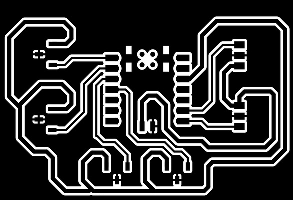
Big rectangle area will be removed and so could lead to longer cutting time
Only the clearance (i.e. the gap between the trace and the rest of the copper area) will be removed; decreasing significantly cutting time
In KiCad, this can be done with the following steps :
- Go to File → Plot.
- Choose SVG as the plot format
- Select the layer of interest (e.g. copper top layer).
- Check the option for “Negative Plot” so that traces will appear white (kept) and the areas to remove will appear black
Further processing can be done in software like Inkscape to reduce the default black areas exported from KiCad.
| Design | Result |
|---|---|
 |
 |
1 pass = 60 mins cutting time
| Design | Result |
|---|---|
|
 |
1 pass = 10 mins cutting time
SVG files exported from KiCad or modified in Inkscape may be interpreted differently by LaserPecker Design Space (LDS)
It was later observed that there can be compatibility issues when reading SVG files from KiCad or Inkscape in the LSD, so converting the design to PNG may be necessary. It is important though to verify that the physical dimensions are correct before starting the laser job because of the difference between raster and vector-based format.
Documentations on setting up the physical machine of the LaserPecker 3 are readily available online (e.g. focal point of the laser). The following settings for the laser cut were used:
- Material : copper
- Passes : 5
- Power : 100
- Depth : 90% (controls the intensity of the laser ablating (removing) the material)
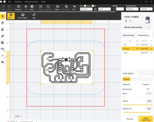
The PCB images shown above are the results of these settings.
Users may try 1 pass at a time and use a multimeter to check if the copper has been fully removed electrically. If there is any slippage or misalignment, refer back to the laser preview before continuing.
It is interesting to note that past documentation suggests that copper removal using fiber lasers can be achieved in just a few passes at similar depth settings (e.g., 4 passes at 90%). In contrast, additional passes were experimented further with using the diode laser (e.g., 7 passes), but the copper was still not fully removed. From this, it can be concluded that the diode laser alone is insufficient for complete copper removal.
PCB design submission to a board house
Designs are typically sent to board houses when producing more than 10 boards or when the minimum trace spacing is around 0.125 mm, finer than what can be reliably achieved with in-house milling (~0.38 mm). For this run, a test is being done to verify the order workflow.
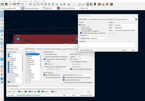
PCB manufacturers require detailed design data to fabricate a board accurately. The key files typically include: :
- Gerber files : Describe the 2D patterns of each PCB layer, including copper traces, pads, silkscreen text, border outline, etc
- Drill files : Lists the location and size of every hole in the PCB. This includes vias, through-hole pads, and mounting holes.
At the time of writing, KiCad version 9 is being used. The screenshot below follows the official website recommendation for exporting the aforementioned files. For full and up-to-date details, please refer to the online documentation.
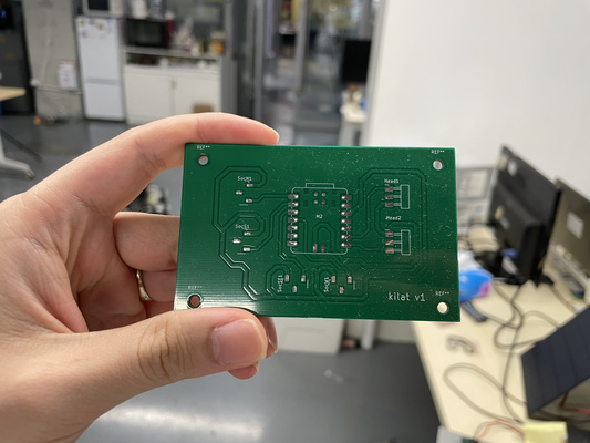
JLCPCB was selected for this order simply due to its location in Shenzhen, China and no other reason. The PCB was ordered through the manufacturer’s online platform. By uploading the zipped Gerber and drill files, the platform automatically detected the design parameters and pre-filled or suggested appropriate specifications. The remaining options were then selected manually, with notes provided to explain the reasoning.
| Parameter | Selected Option | Notes |
|---|---|---|
| PCB/PCBA | PCB | PCBA includes components soldered onto the board; only the bare PCB is needed |
| Surface finish | LeadFreeHASL | More environmentally friendly than HASL (with lead) |
| Electrical test | Flying Probe Random Test | Free of charge and so nice to have a "four-eye check" |
The remaining steps are pretty straightforward and so not further documented here.
Yes, you need a mandarin name for the shipping address details 
For the parameters selected above the overall cost is $5.56, with the following breakdown :
- 5 pieces of PCB : $3.20
- Shipping : $2.04
- VAT : $0.32
The following was the timeline of the whole process :
- Order : 17th of March
- Production : 17th of March
- Shipment : 19th of March
- Final delivery : 24th of March
The expected delivery time was likely around 2-3 days considering the close proximity of the factory at Zhuhai to Shenzhen. However, the delivery in the end took 7 days (i.e. 24th). **The delay was later found out due to the specific delivery service compoany used in which recipient must actively accept the delivery call. If call is not answered, the personnel will not leave the package unattended (e.g. at the front door).
Fabrication and testing
Soldering and Desoldering Techniques: How-To and Tips
Soldering with Lead (Manual)
-
Heat & Squish
- Apply a small amount of flux to the pad or wire.
- Place solder on the pad.
- Heat the solder with a soldering iron until it melts.
- Gently press (“squish”) the component lead or wire into the molten solder.
- Remove heat and allow the solder to solidify.
-
Tin & Heat
- Heat the wire or PCB pad slightly.
- Apply a thin layer of solder to tin the surfaces.
- Place the tinned wire/component onto the pad.
- Reheat briefly until the solder flows and forms a solid joint.
-
- Apply solder paste to PCB pads using.
- Place surface-mount components onto the paste.
- Heat the board gradually using a hot plate or hot air gun until the solder melts and forms joints.
- Allow the board to cool naturally.
Soldering with Solder Paste (Reflow)
- Note:
Hot plates are suitable for FR4 boards, while FR1 boards (poor thermal conductors) often require heating from above using a hot air gun (top-down method).
-
Desoldering Techniques
-
Using a Solder Pump
- Heat the solder joint until the solder melts.
- Place the solder pump nozzle over the molten solder.
- Activate the pump to suck up the solder.
- Repeat if necessary until the component can be removed.
-
Using a Desoldering Wick
- Heat the solder joint with a soldering iron.
- Place a desoldering braid (wick) on the joint.
- Allow the wick to absorb the molten solder.
-
It is better to prioritise smaller components first, followed by larger components, to ensure accessibility during soldering
Wire jumpers or 0 Ω resistors can be used to connect traces if there were mistakes during the design or to provide bypasses that are sometimes difficult to implement
The PCB produced using the copper milling is used for the test. Thought process/steps are as follows :
- Connectivity test
- Soldering process : Soldering iron and solder paste with a heatbed (possible by FR4 substrate)
- Final connectivity test : Confirm proper circuit operation
In general the same process is also applied to the industrial PCB.
Connectivity test
The connectivity test has been already explored at Week 6 : Electronics design and therefore will not be explained in detail here. It is however interesting to point out that the grounds of the components are connected together, except the microcontroller's. This differs from the industrial PCB as the ground plane is connected together beneath the solder mask (note that it's non conductive and does not provide electrical connectivity). Therefore in this case the jumper wire was used as a "bridge" to the common ground.
Visual illustrations could be seen further below.
Soldering process
For this test, only 1x SMD socket, 1x SMD pin headers, and a microcontroller (in this case XIAO ESP32C3) is used for test purpose. The method using the heatbed with solder paste is available online ; however it was later realised that the pin headers only have one side pad and so it reduces significantly the mechanical stability (i.e. it always want to topple down to the other side). Therefore the "heat and squish technique" is applied to ensure good adhesion during soldering.
Remove residual adhesives of the PCB used during the CNC milling before soldering at the heatbed
Use components with pads on both sides to improve mechanical stability
The 5V power rail connection especially for the servo was not included in the original PCB design and so a USB-C board is connected to the main PCB via the jumper wire. The wire stripper and is first used to expose the conductor and then the "tin and heat" technique is applied (unfortunately the press part to the board is not documented) to make a proper bonding between the two parts.
Final connectivity test
The final step is to do another connectivity test again as there is a possibility of excess solder or shift of components that might cause unintended short circuits.
P.S. this is arguably the most frustrating part, especially when the beeping indicates a connection in exactly the place the user were hoping it wouldn’t be.
However, if everything works well. Voila!
The PCB design file is available in Week 9 : Electronics Production.