Week 9
Input Devices
This week, I explored the integration of input devices with PCBs, focusing on how sensors and switches interact with microcontrollers to receive and process data. Input devices such as buttons, sensors, and encoders play a crucial role in capturing external signals and converting them into meaningful information for embedded systems.
I worked on understanding the electrical characteristics, communication protocols, and interfacing techniques required to connect these devices to a microcontroller. Additionally, I examined signal conditioning methods, power considerations, and programming approaches to ensure accurate data acquisition. Through hands-on implementation and testing, I gained practical insights into designing efficient input circuits and troubleshooting common issues.
This week, I am working with two Electronic Production as part of assignments:
Group Assignment
Individual Assignment
Group Assignment
As part of the group assignment, Dr. Sujit and I conducted a study that included the following tasks:
1. Integration of Input Devices – Connect and interface various input devices with a PCB.
2. Circuit Design – Design and implement a reliable circuit for input device integration.
3. Sensor Interfacing – Understand and apply techniques for interfacing sensors with a microcontroller.
4. Microcontroller Programming – Develop and test firmware to process input data effectively.
5. Reliable Connections – Ensure stable and efficient connections between components.
6. Data Analysis – Capture, interpret, and utilize data from input devices.
The group assignment is linked here
Individual Assignment
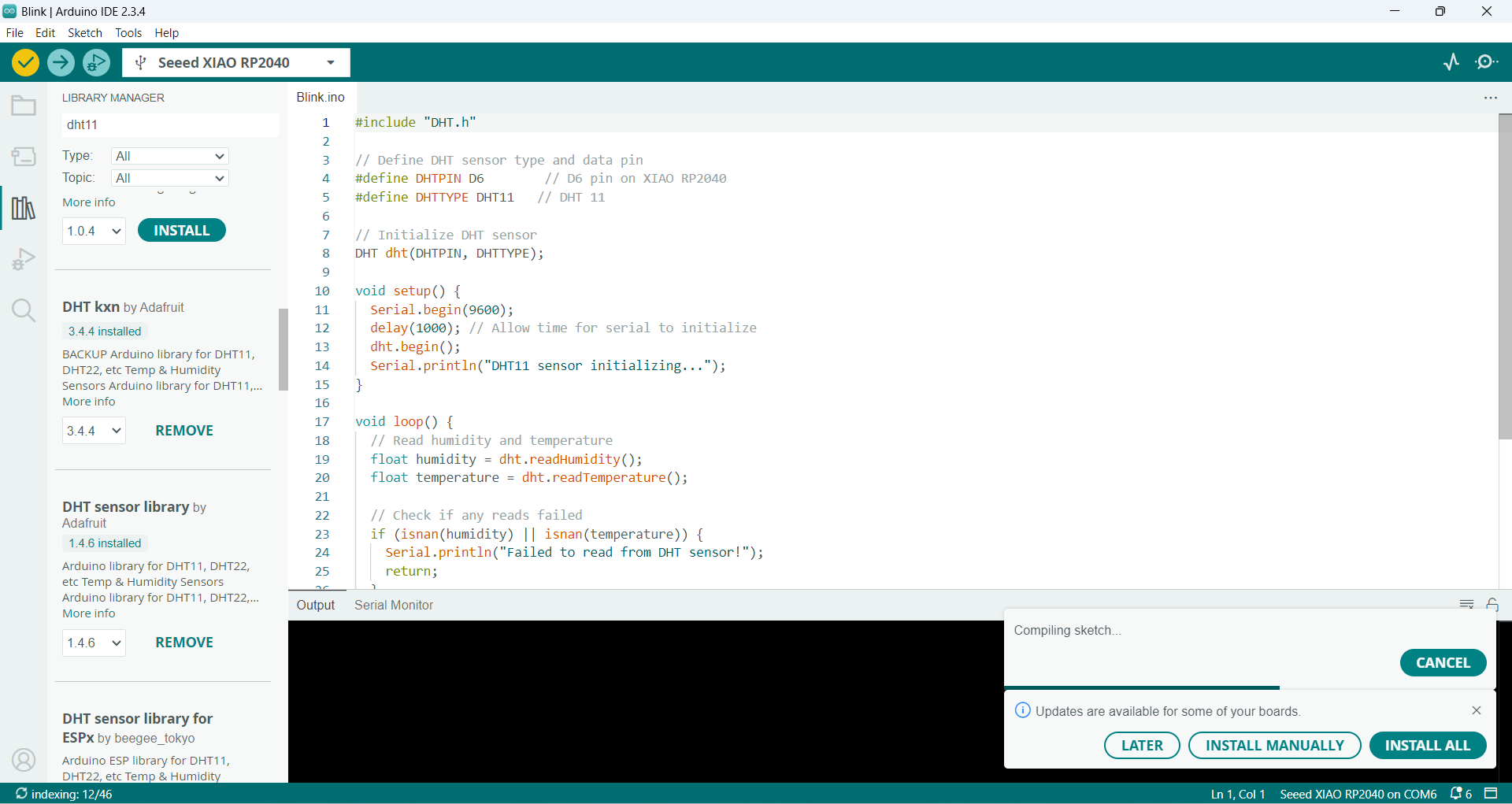
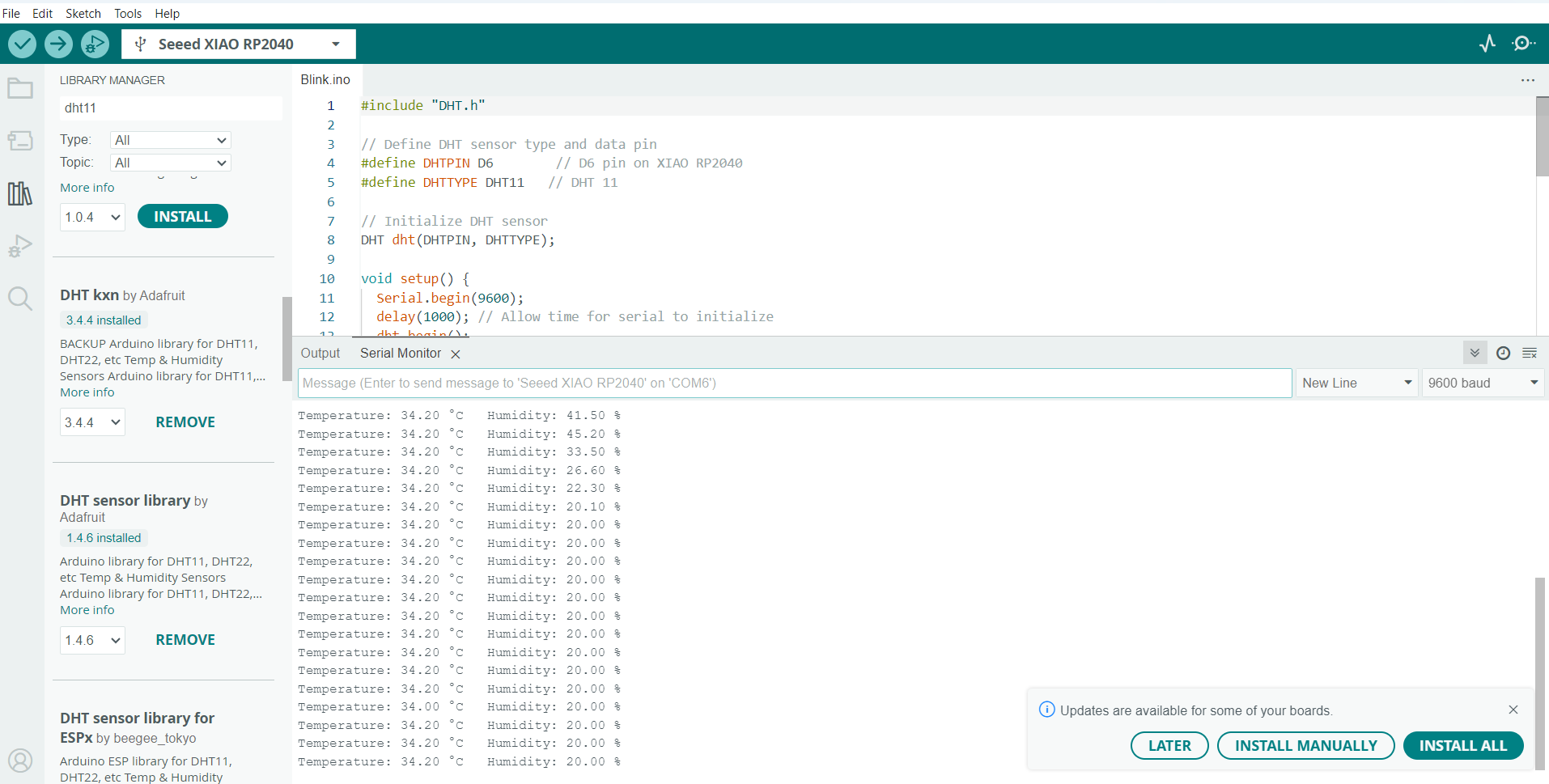
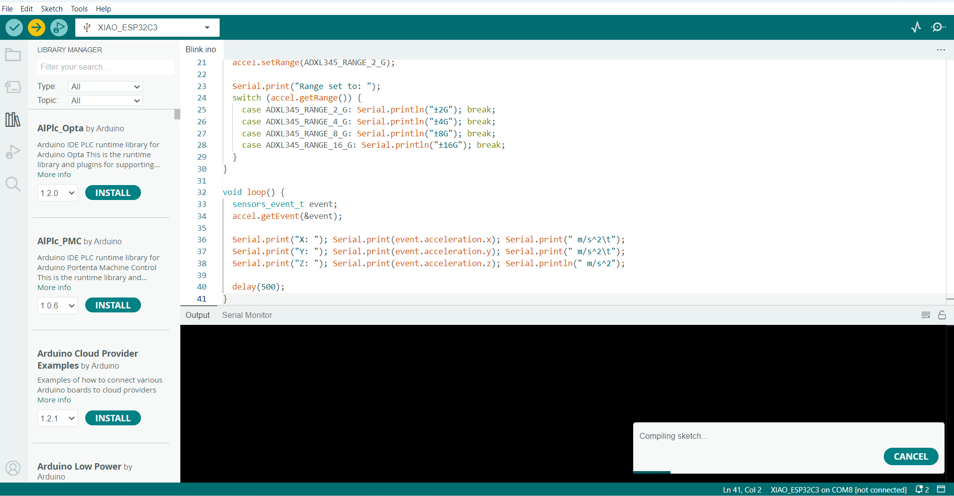
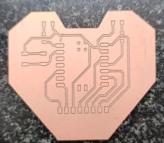
In my individual assignment, I focused on designing and fabricating a PCB to interface with various input devices. The objective was to develop a functional circuit that could effectively capture and process data from sensors and switches using a microcontroller.
I began by designing the PCB using an EDA tool, ensuring proper routing and component placement. After finalizing the design, I proceeded with milling the PCB and assembling the necessary components. Once the hardware was ready, I programmed the ESP32-C3 microcontroller to read data from the connected input devices
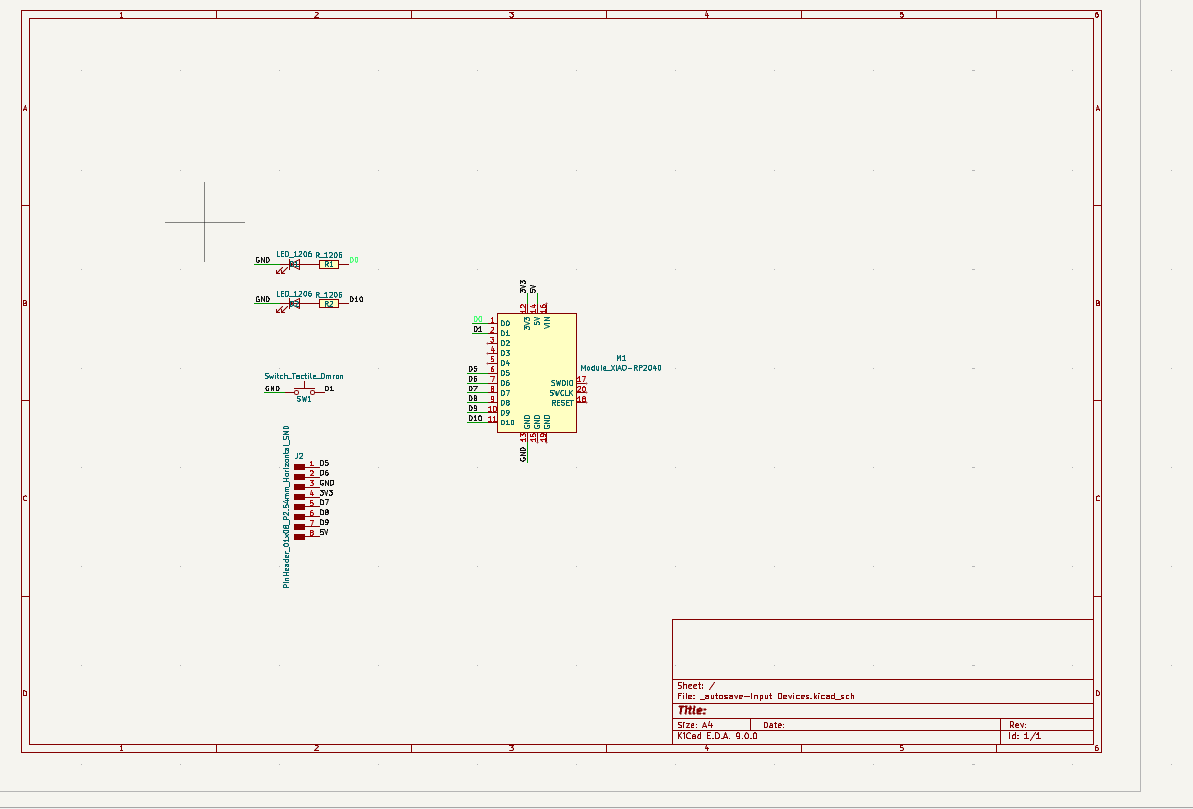
Design of PCB with KICAD software
As I explained in Week Six, I learned to use this software for PCB design. It is open-source and easily available online. Using this software, I designed a PCB.
The schematic diagram explains that I used the Xiao RP2040 board for the PCB design.
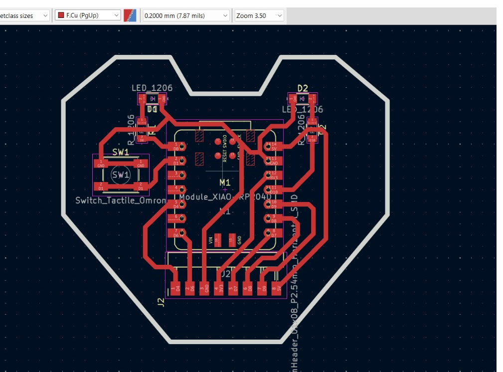
Then, I opened the PCB editor and used the "Route Track" command to make the necessary connections, ensuring that the PCB functions properly.
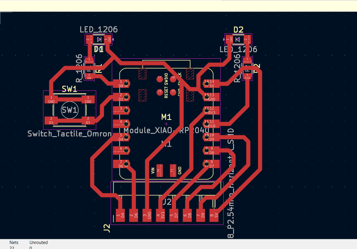
Then, I used the Edge Cuts layer, selected the Draw Line tool, and created the PCB outline.
In the next step, the file needs to be saved for PCB fabrication. The files are saved in two ways: one for traces and another for the outline cut.
To save the file for traces:
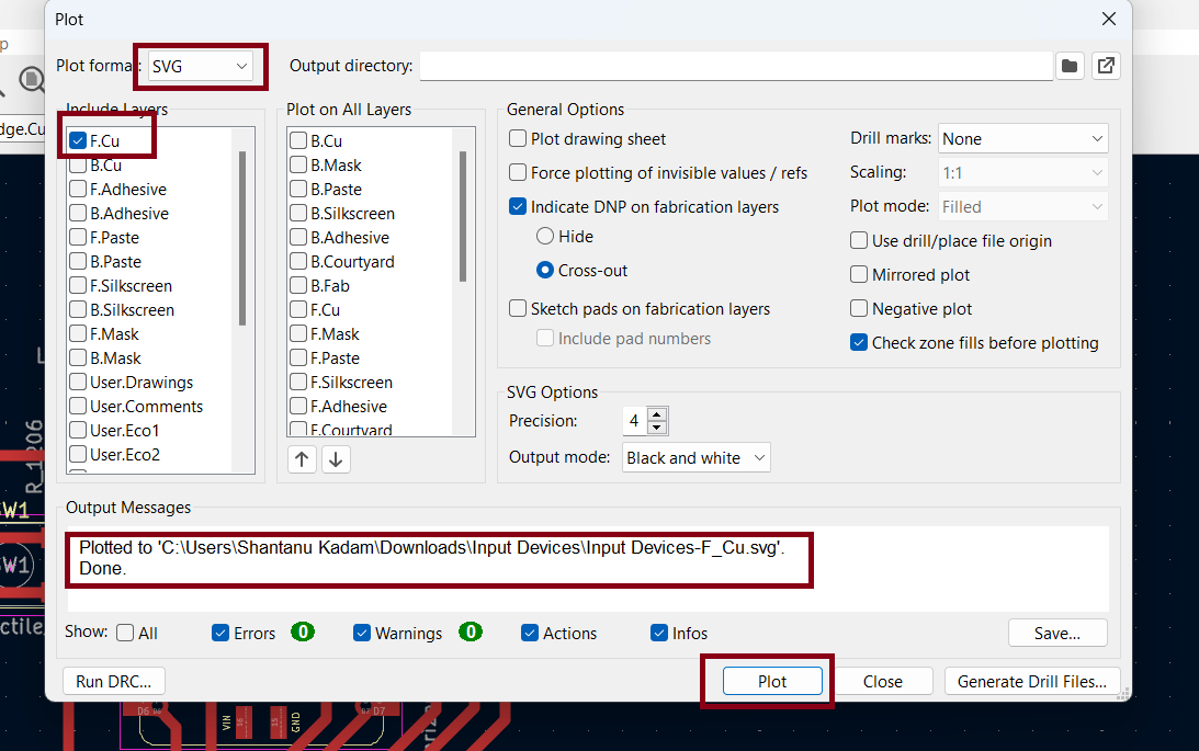
1. Go to the File menu and select Plot.
2. In the Plot window, choose SVG as the output format.
3. Select F.Cu (the front copper layer).
4. The output message will display the save location of the file.
5. Finally, click Save to store the file.
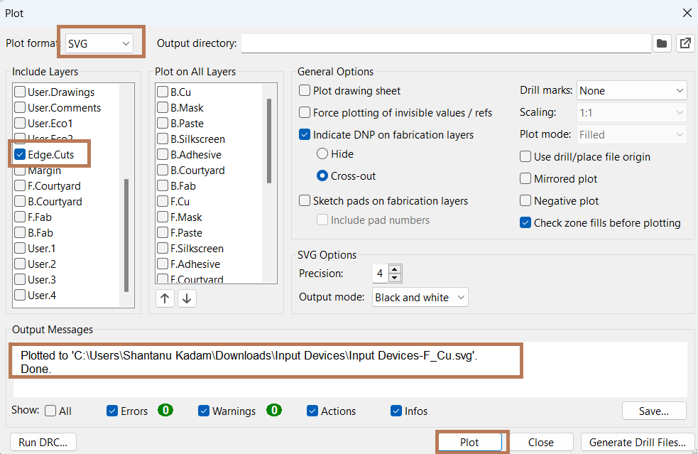
The same procedure is repeated for the edge cut, except instead of selecting F.Cu, choose Edge Cuts.
1. Go to the File menu and select Plot.
2. In the Plot window, choose SVG as the output format.
3. Select Edge Cuts instead of F.Cu.
4. Click Plot to generate the path for saving.
5. Finally, click Save to store the file.
All the aspects related to the schematic and PCB editors are not explained in detail here.
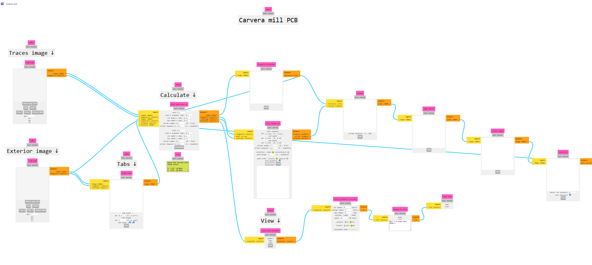
Generate Toolpath for PCB Milling
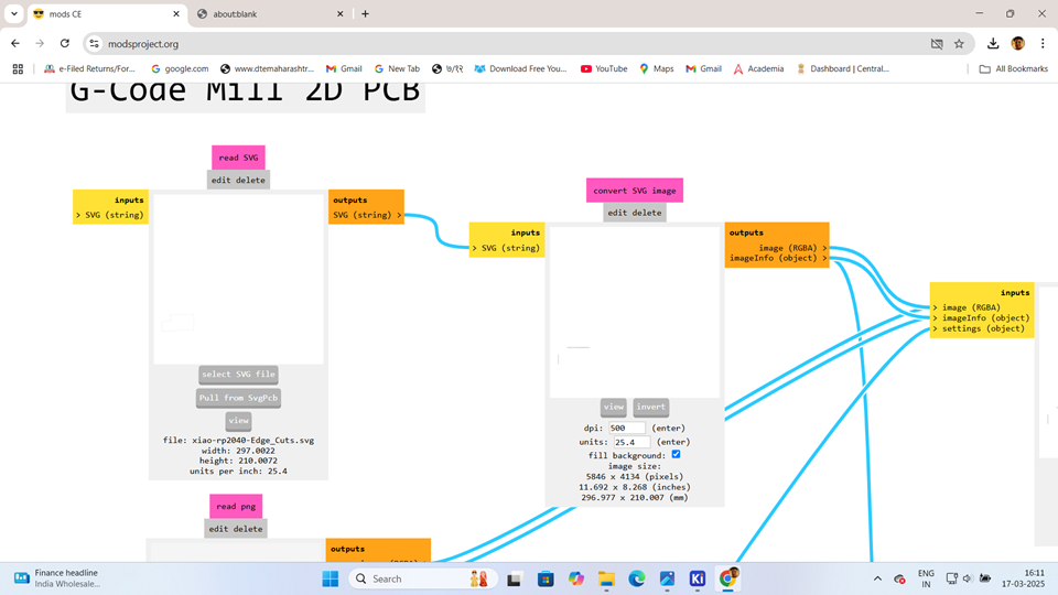
To generate the toolpath for CNC milling and create the PCB, I used the Mods Project online platform.
1. Open the Mods Project website.
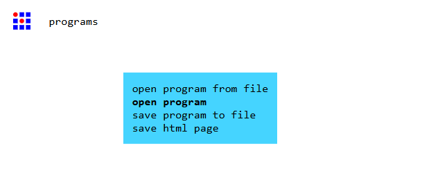
2. Once the website loads, the main window appears.
3. Then right click and from the available options, select program.
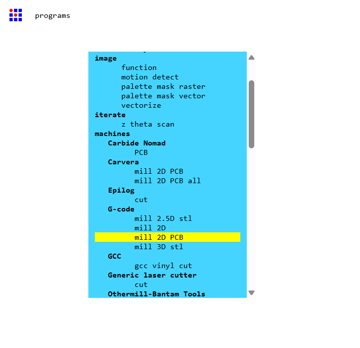
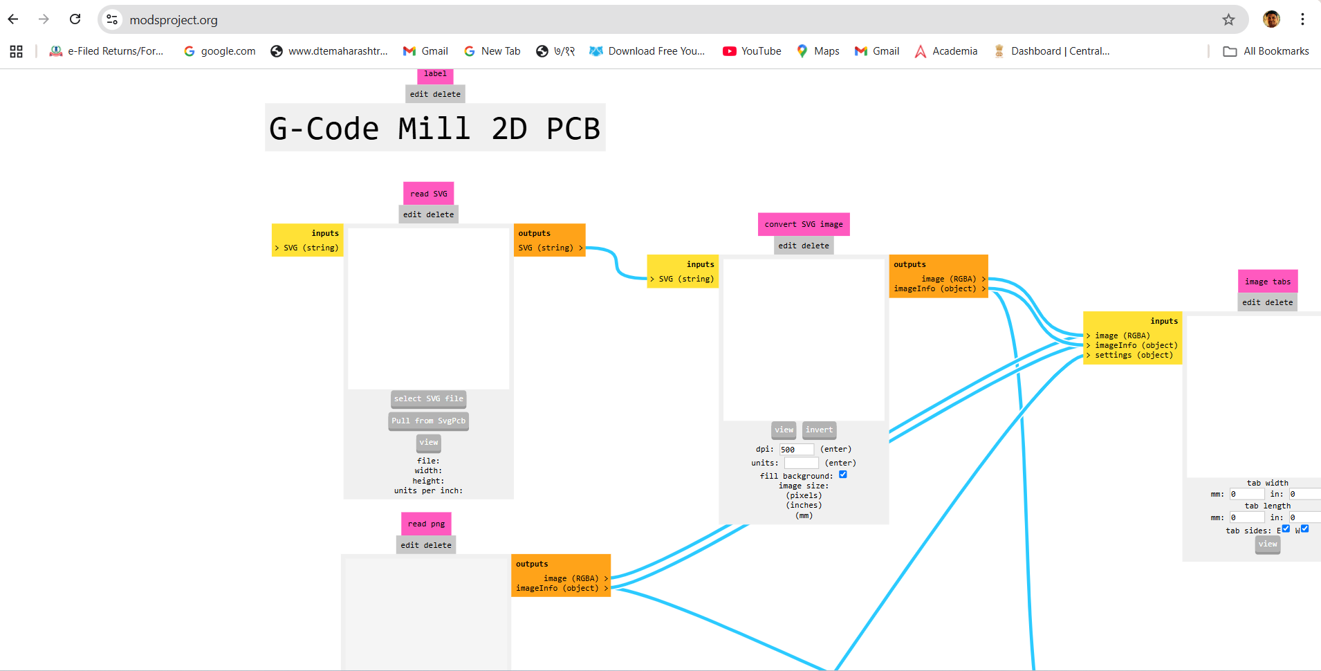
As the program opens, I scroll down and, under the G-code section, select Mill 2D PCB.
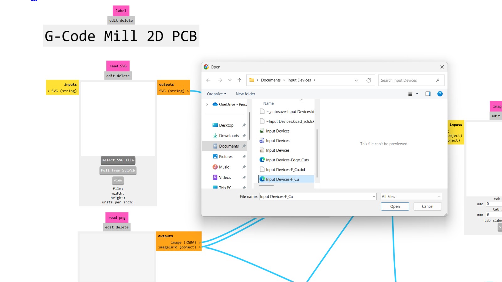
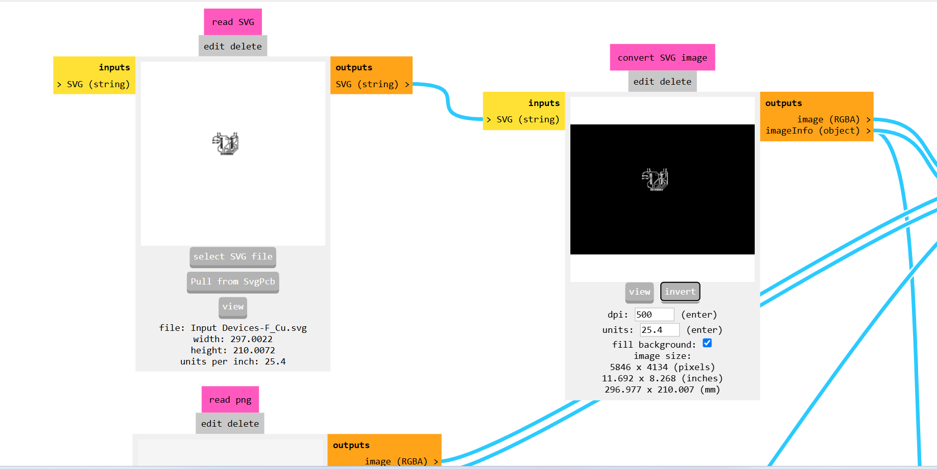
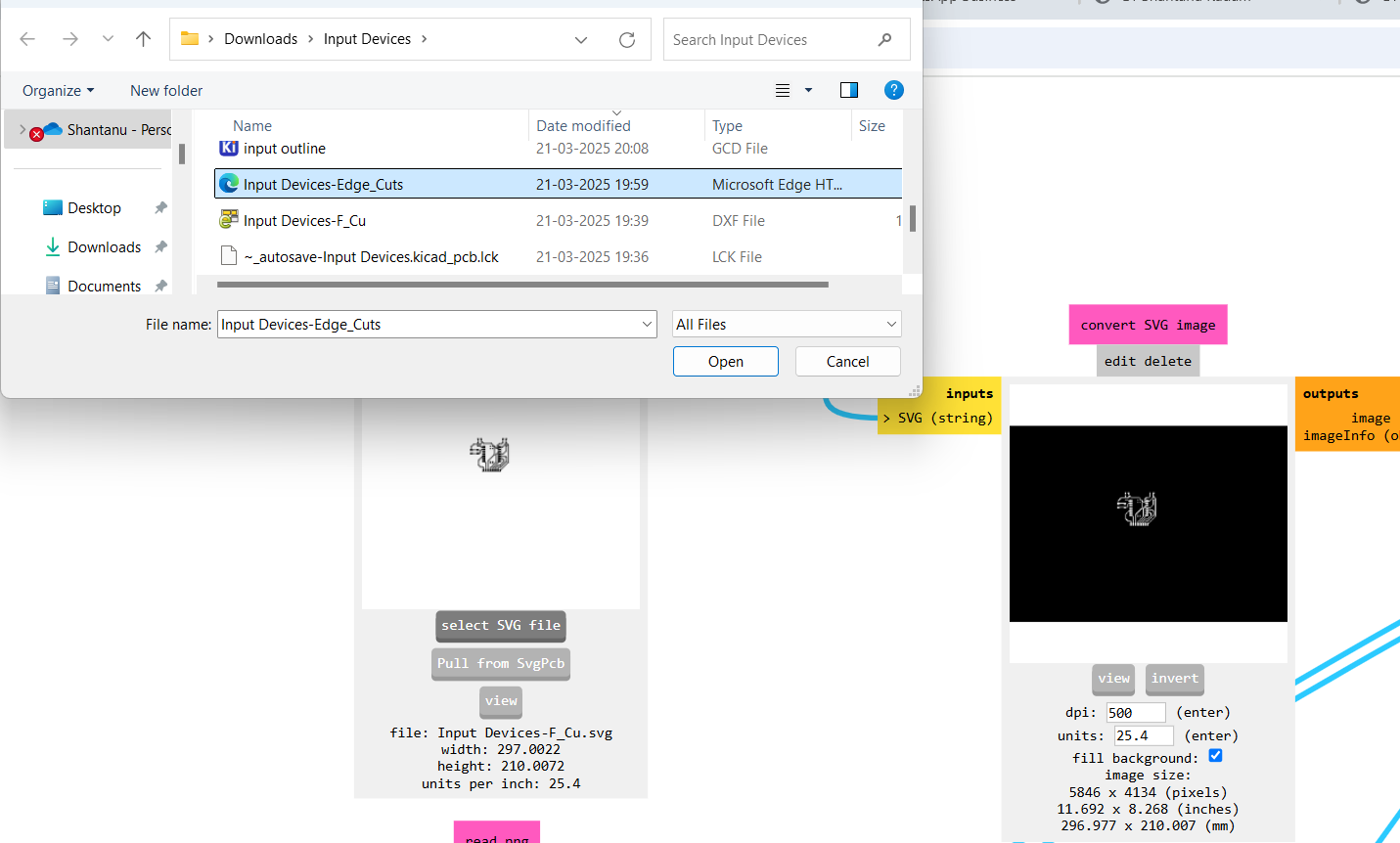
Then, go to Read SVG and select the SVG file. Then go to desired location and select .svg file format those are saved in KICAD software.
After selecting the file, press open to preview it.
Then, the preview appears in the Select SVG menu. Then, navigate to the "Convert SVG Image" section and select the "Invert" option.
Then, go to Set PCB Default and select Isolate Traces.

No changes are made in the Isolate Traces settings.
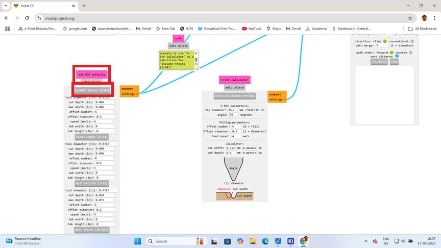
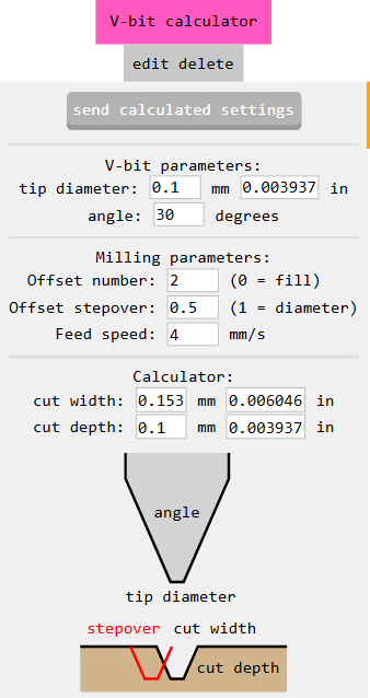
It looks like you're configuring the V-bit parameters for your CNC machining.
Open the V-bit Calculator in your software.
Set the parameters:
1. Tip Diameter: 0.1 mm
2. Angle: 30°
3. Cut Depth: 0.1 mm
4. Click on "Send Calculated Setting"
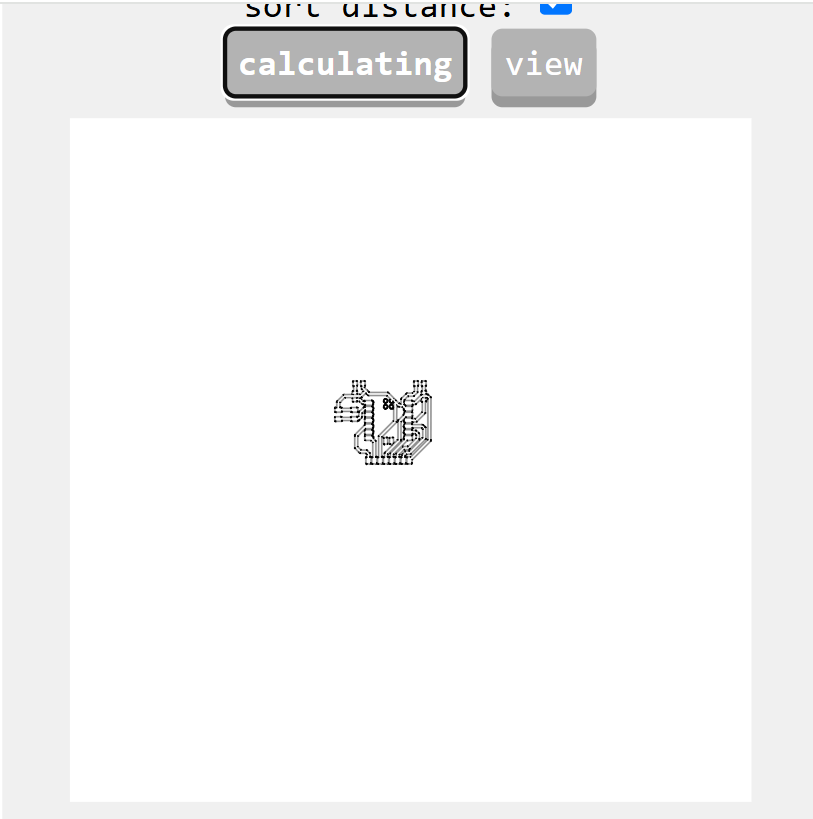
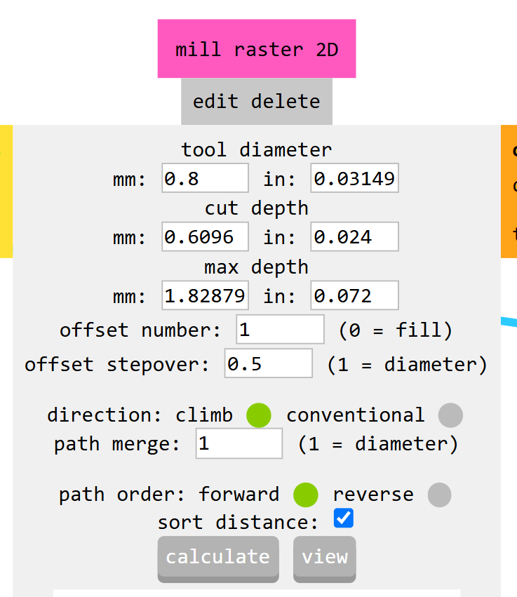
Then goes into mill raster 2d option. Change the Tool Diameter to 0.1 mm. Then, press the "Calculate" option. Once the calculation is complete, the file will be downloaded to the "Downloads" section.
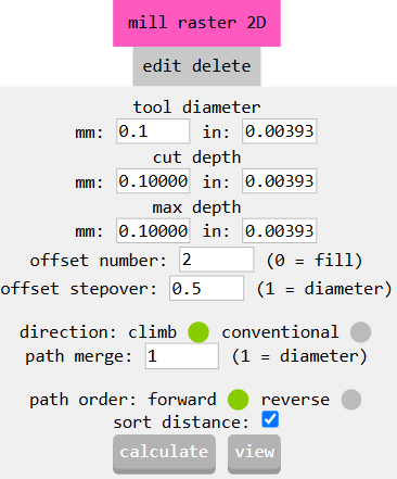
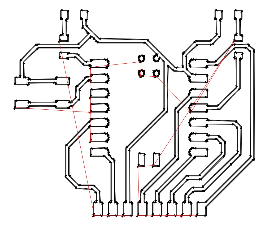
Then click on the view option.
Click on the Calculate Button to generate the toolpath.The software will then generate the PCB milling file in .nc format.file is save in Downloads.Go to the "Downloads" folder and open the file. This file shows the toolpath.
After that click on the calculate option it will generate the pcb milling file in . nc format.
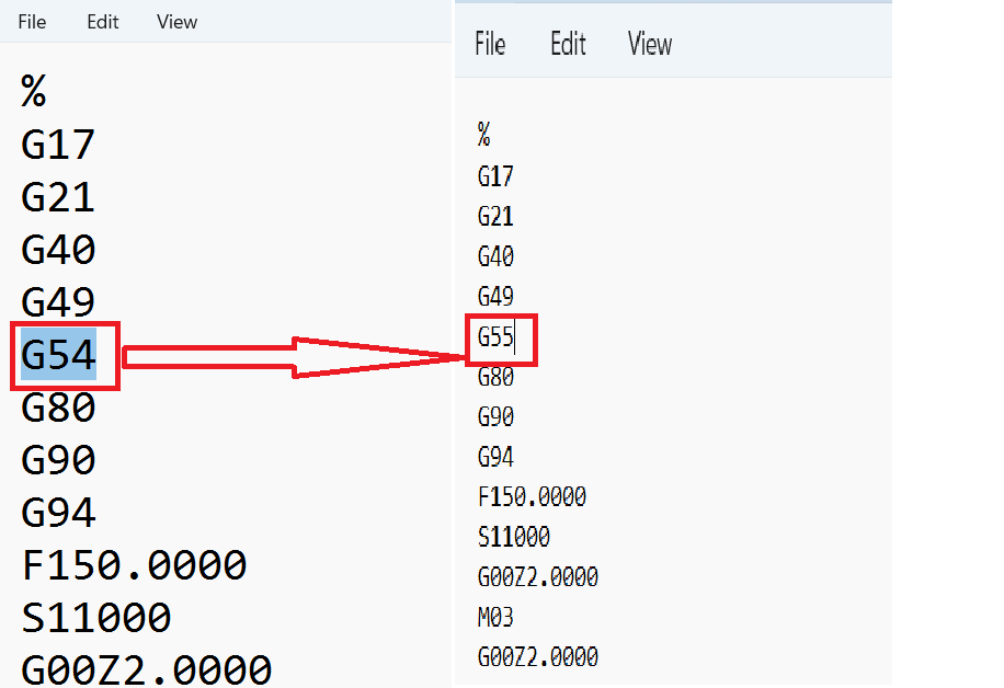
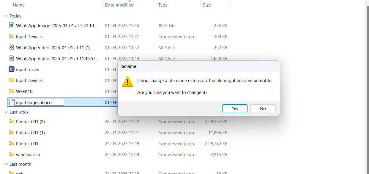
Navigate to the Downloads folder and locate the generated .nc file. Rename the file by changing its extension from .nc to .gcd.
Once the file is saved in the .gcd format, open it using Notepad or a similar text editor. Locate the code G54 and replace it with G55 to adjust the work coordinate system for the PCB milling process. After making the modification, save the file and exit the editor.
Next, access the Mods CE online software to generate the outline toolpath for the PCB milling process.
Then, go to Read SVG again, and in this menu, select the SVG file.
Then, go to Read SVG and select the SVG file. Then go to desired location and select .svg file format those are saved in KICAD software. Then select the edge_cut file and select open.
Then, go to Set PCB Default and select millout line (1/32).
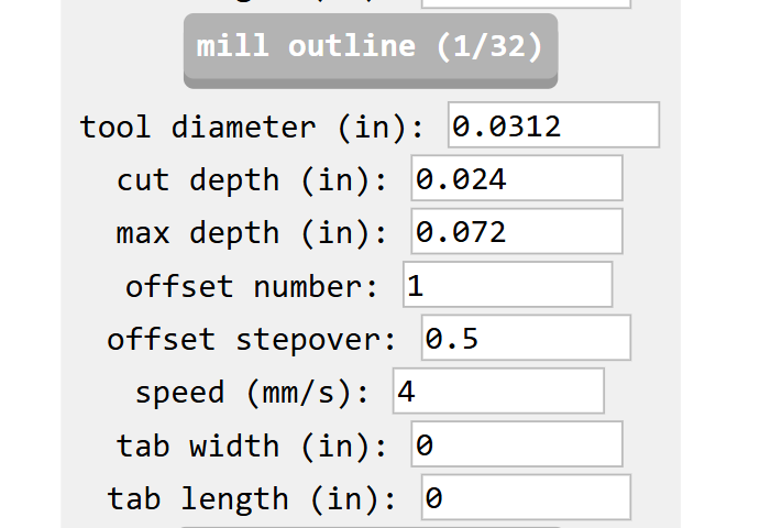
Without making any changes, go to Mill Raster 2D, change the tool diameter to 0.8mm, and save the changes.
After that click on the calculate option it will generate the pcb milling file in . nc format.
Navigate to the Downloads folder and locate the generated .nc file. Rename the file by changing its extension from .nc to .gcd.
Once the file is saved in the .gcd format, open it using Notepad or a similar text editor. Locate the code G54 and replace it with G55 to adjust the work coordinate system for the PCB milling process. After making the modification, save the file and exit the editor.
CNC Milling Process
Once the trace and outline files are generated, the PCB design is ready for manufacturing.
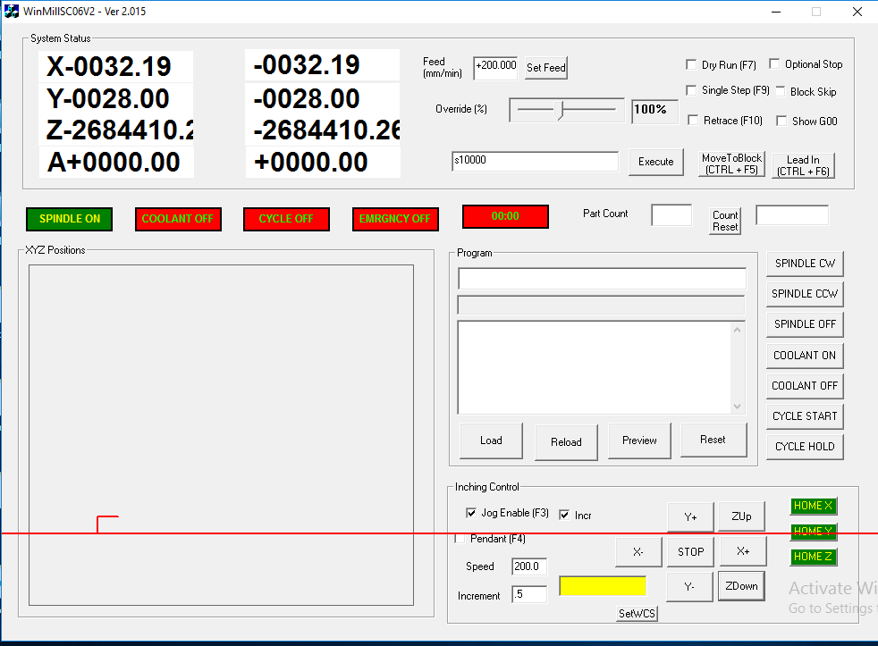
Then, proceed to the PCB milling machine, where the machine software is launched. Initially, the startup window is displayed.
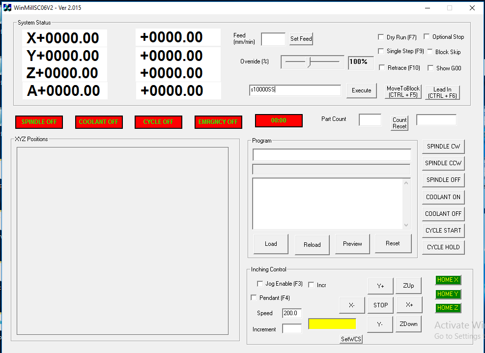
Next, it is important to set the origin point. To do this, first, click on the "Jog Enable" menu, then select "Incremental." Set the desired increment value, and use the -X, +X, -Y, +Y, Z-up, and Z-down controls to position the spindle accurately.
When go into the Set WCS menu and set X0, Y0, Z0, you are likely defining a new origin point for design.
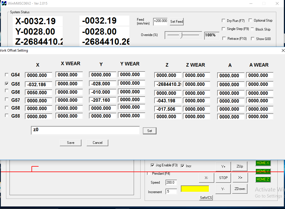
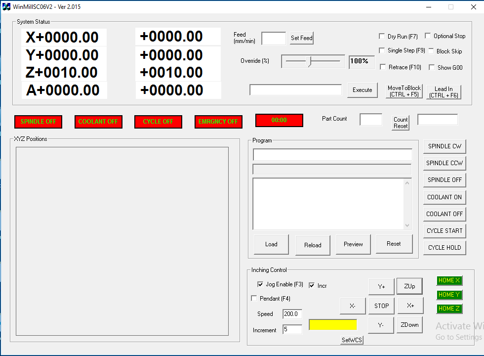
Then, click the Save button to set the origin for the PCB milling process. The screen will display the coordinates X0, Y0, Z0, confirming that the new reference point has been established.
Next, navigate to the Increments setting, configure it as needed, and click Z-Up to move the tool upward.
Then, navigate to the Load menu and select the program from the desired location.
Load the traces program to initiate the cutting process for the PCB traces.
Then, click Cycle Start to begin the milling process.
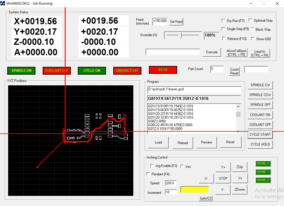
As the milling process begins, the tool rotates at a speed of 10,000 RPM, as specified in the program, and starts cutting the PCB traces.
Once the traces are cut, the program is completed. Next, change the tool from a V-bit to a 0.8mm drilling tool. Then, following the same procedure, load the edge cut program while maintaining the previously set origin and click Cycle Start to begin the process.
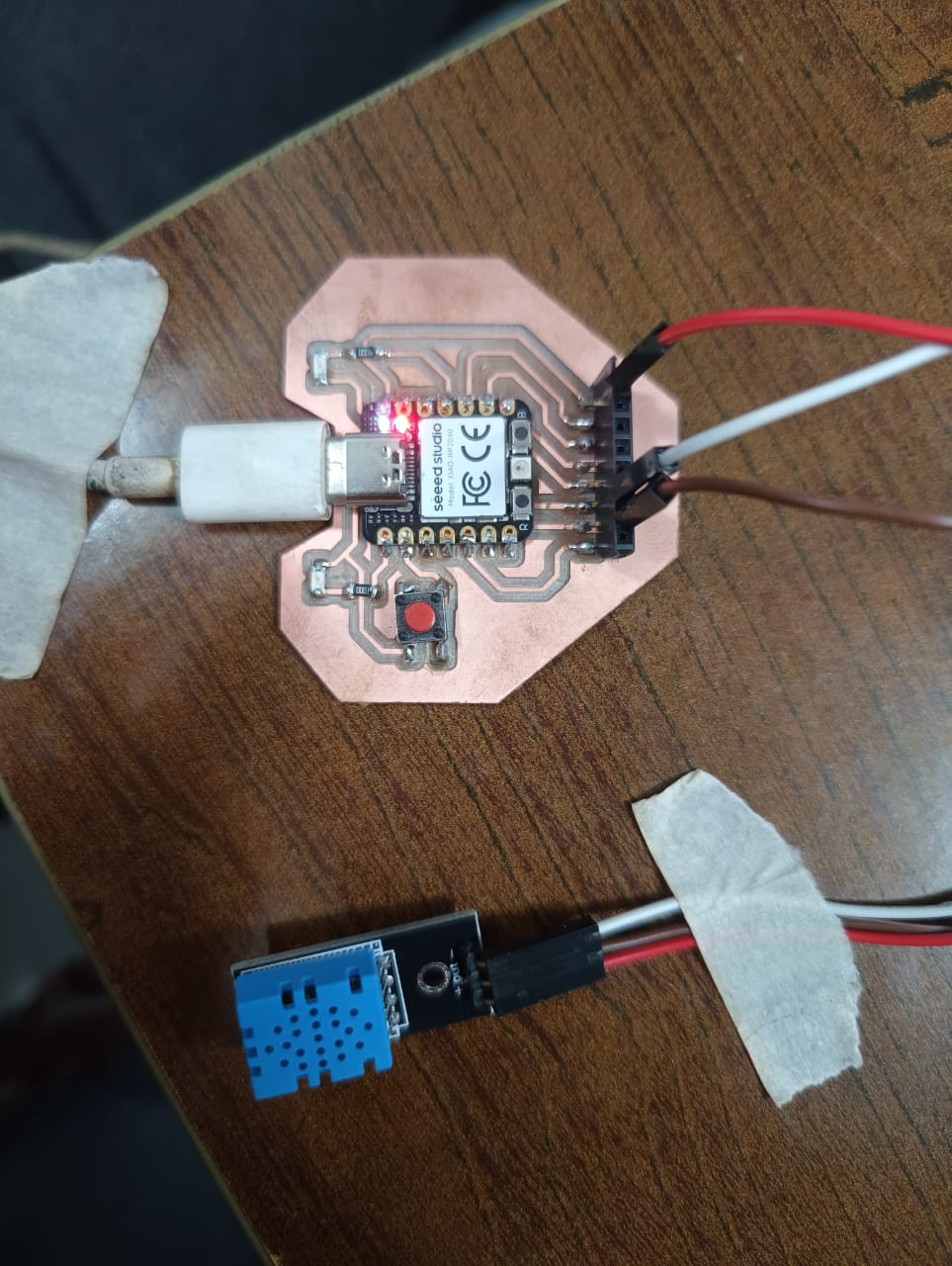
Once the edge cut program cycle is completed, the PCB is ready for the soldering process.
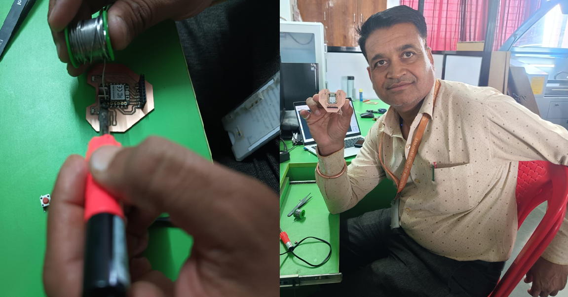
PCB soldering
With the PCB milling process completed, the board is now ready for soldering. In the next step, the soldering process will be carried out.
In the soldering process, I connected the push button, resistor, LED, connector, and XIAO RP2040 board to the PCB.
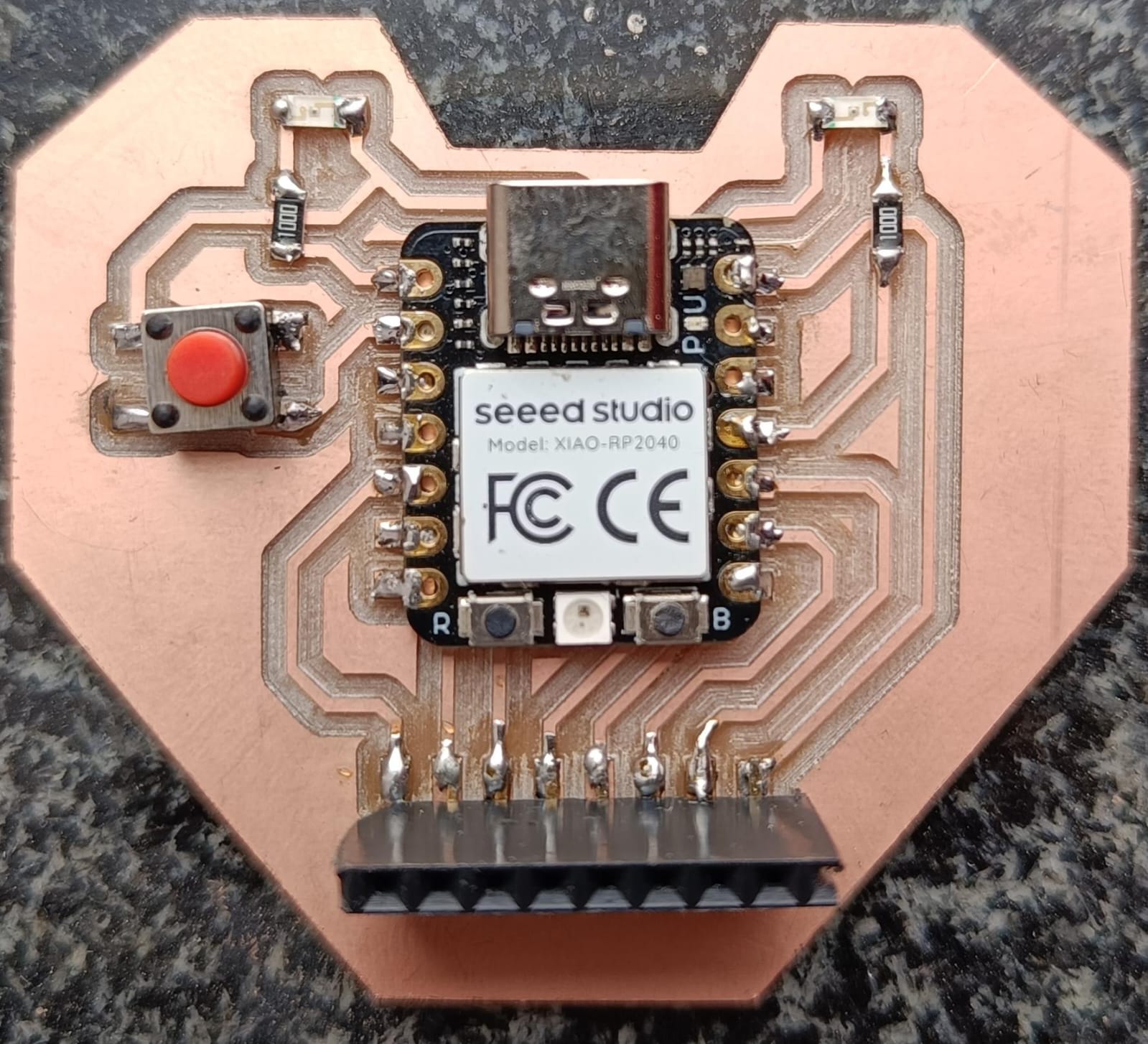
Hero Shot
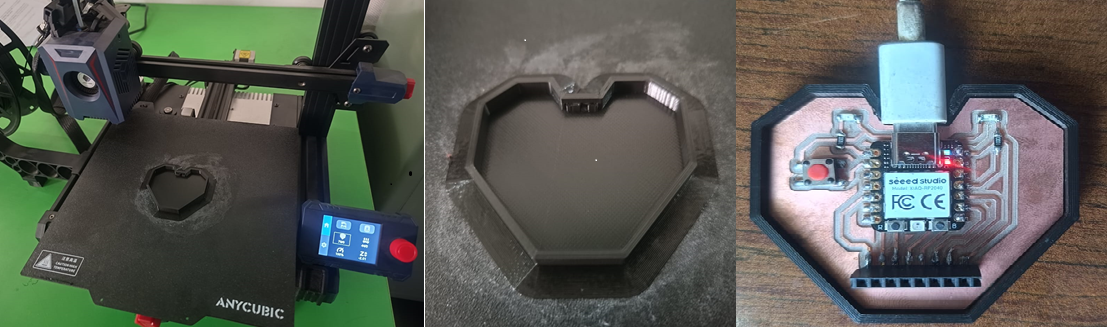
After successfully manufacturing the custom PCB for the Seeed Studio XIAO RP2040, the next step in my project is to design and fabricate a case for the board using 3D printing.Case will also enhance the overall aesthetics and usability of the device. The case will be designed in CAD software, ensuring precise dimensions and proper cutouts for the USB port, pin headers, and any onboard components. Once the design is finalized, it will be 3D printed using a suitable material like PLA to provide a durable and functional housing for the custom PCB
Input Devices PCB Working
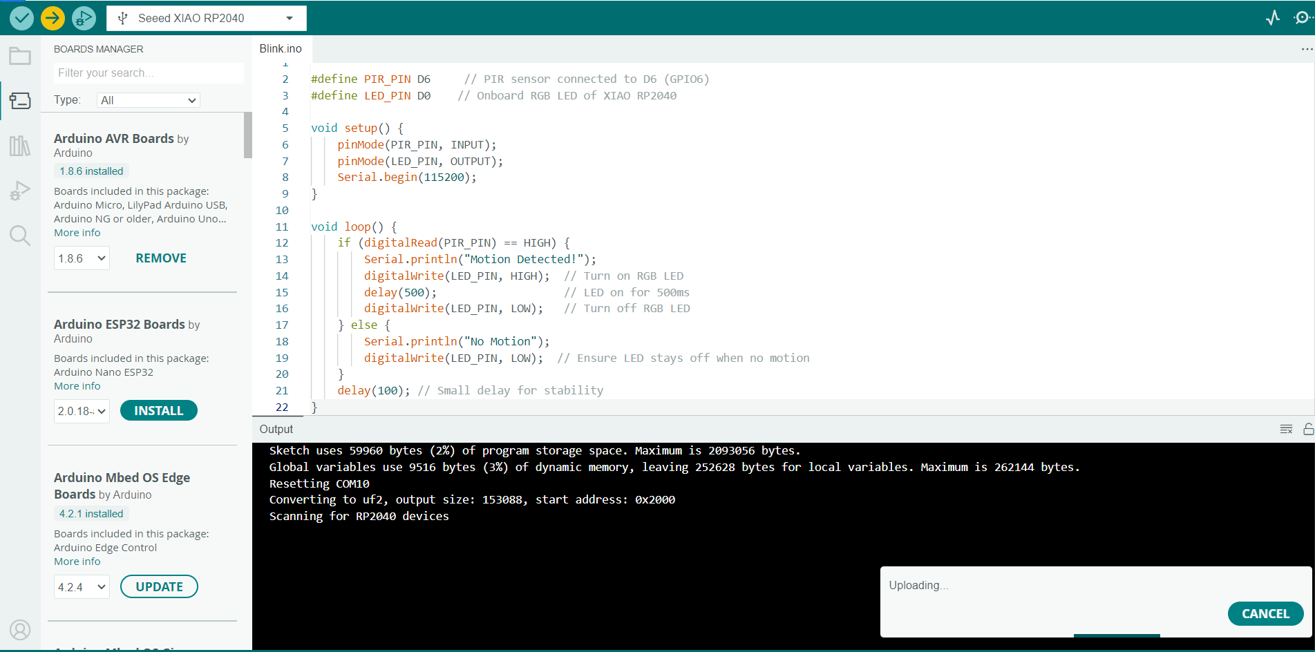
As the PCB is ready, the next step is writing a program for PIR (Passive Infrared) sensor.
By detecting infrared (IR) radiation released by objects, especially living things, inside its field of vision, an electronic sensor known as a PIR (Passive Infrared) sensor can identify motion. PIR sensors passively monitor changes in infrared radiation rather than sending out signals like active sensors do. Initially, LEDs will blink simultaneously.
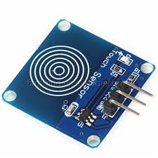
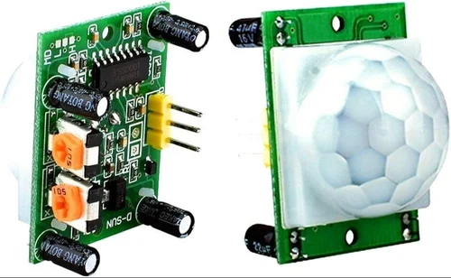
The image shows a PIR (Passive Infrared) Motion Sensor Module, widely used in automation and security applications to detect human movement. The most common model of this type is the HC-SR501, which senses infrared radiation emitted by objects, particularly human bodies, within its field of view. The dome-shaped white component is a Fresnel lens, which focuses infrared signals onto the underlying pyroelectric sensor to detect motion.
This module operates typically at 5V DC and provides a digital output that goes high (3.3V or 5V depending on model) when motion is detected. It has three pins: VCC, GND, and OUT. The VCC is connected to a 5V supply, GND to ground, and OUT provides the motion signal to microcontrollers or other circuits. Two orange-colored potentiometers are available on the board—one to adjust the sensitivity (detection distance) and the other to set the delay time for how long the output remains high after motion is detected.
This PIR sensor typically covers a range of 3 to 7 meters and a detection angle of approximately 120 degrees. It is energy-efficient and only responds to moving infrared sources, making it ideal for applications like automatic lighting systems, burglar alarms, smart home projects, and occupancy detection. Its compact size and ease of interfacing make it popular in both DIY and industrial electronics.
#define PIR_PIN D6 // PIR sensor connected to D6 (GPIO6)
#define LED_PIN D0 // Onboard RGB LED of XIAO RP2040
void setup() {
pinMode(PIR_PIN, INPUT);
pinMode(LED_PIN, OUTPUT);
Serial.begin(115200);
}
void loop() {
if (digitalRead(PIR_PIN) == HIGH) {
Serial.println("Motion Detected!");
digitalWrite(LED_PIN, HIGH); // Turn on RGB LED
delay(500); // LED on for 500ms
digitalWrite(LED_PIN, LOW); // Turn off RGB LED
} else {
Serial.println("No Motion");
digitalWrite(LED_PIN, LOW); // Ensure LED stays off when no motion
}
delay(100); // Small delay for stability
}
Then uploading it to the XIAO RP2040.