Week 8
Electronic Production
This week, I worked on designing and making printed circuit boards (PCBs) while learning the rules for both in-house production and professional manufacturing. I used an electronic design tool to create a custom microcontroller board with key components needed for embedded system applications.
This week, I am working with two Electronic Production as part of assignments:
Group Assignment
Individual Assignment
Group Assignment
As part of the group assignment, Dr. Sujit and I conducted a study that included the following tasks:
1. Maintain minimum trace width and clearance, ensure proper hole sizes, and consider milling limitations for accurate fabrication.
2. Prepare Gerber files, follow manufacturing specifications, and ensure correct manufacturing.
The group assignment is linked here
Individual Assignment
Design, fabricate, and test a custom microcontroller development board by creating a schematic, milling the PCB, assembling components, programming the board, and verifying its working.
While working on the group assignment, I gained valuable insights of PCB making technology. This hands-on experience allowed me to understand their working principles, operational parameters, and practical applications in digital fabrication.
Design of PCB with KICAD software
As I explained in Week Six, I learned to use this software for PCB design. It is open-source and easily available online. Using this software, I designed a simple PCB.
The schematic diagram explains that I used the Xiao RP2040 board for the PCB design. Additionally, I included a switch, an LED, and a connector. Using all these components, I designed a PCB for this week.
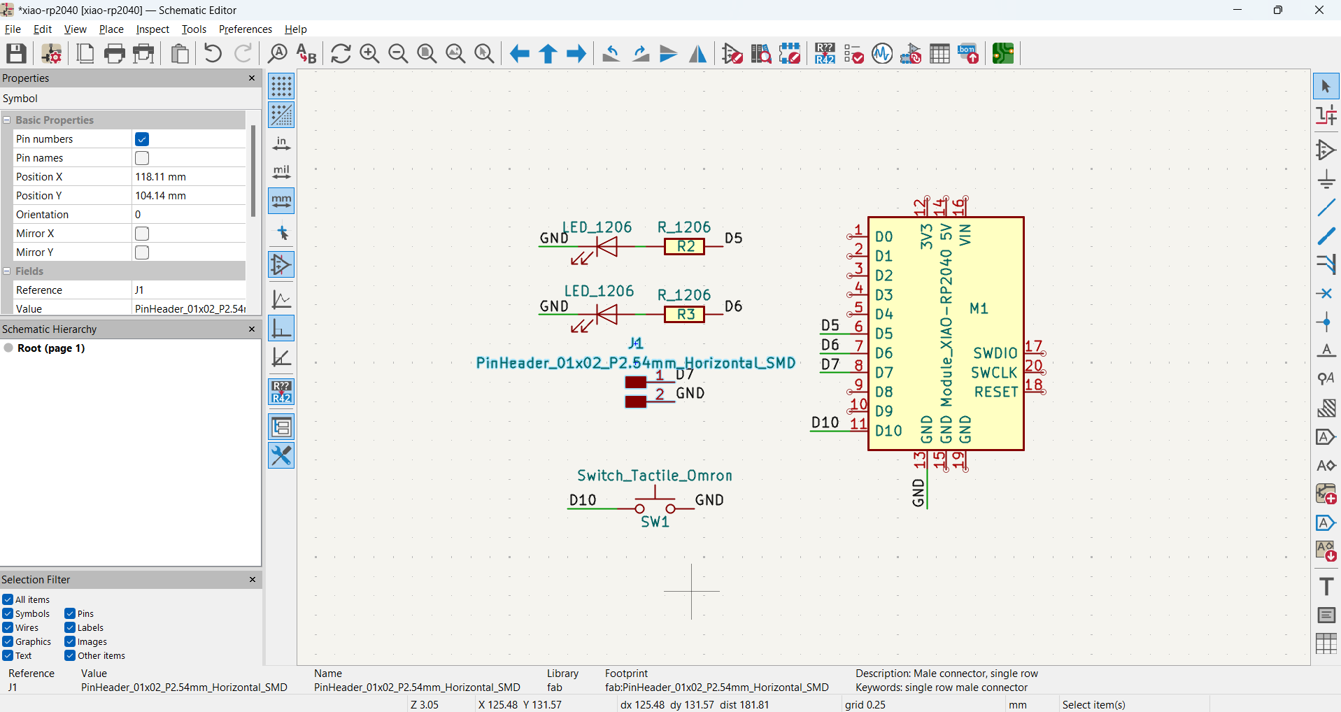
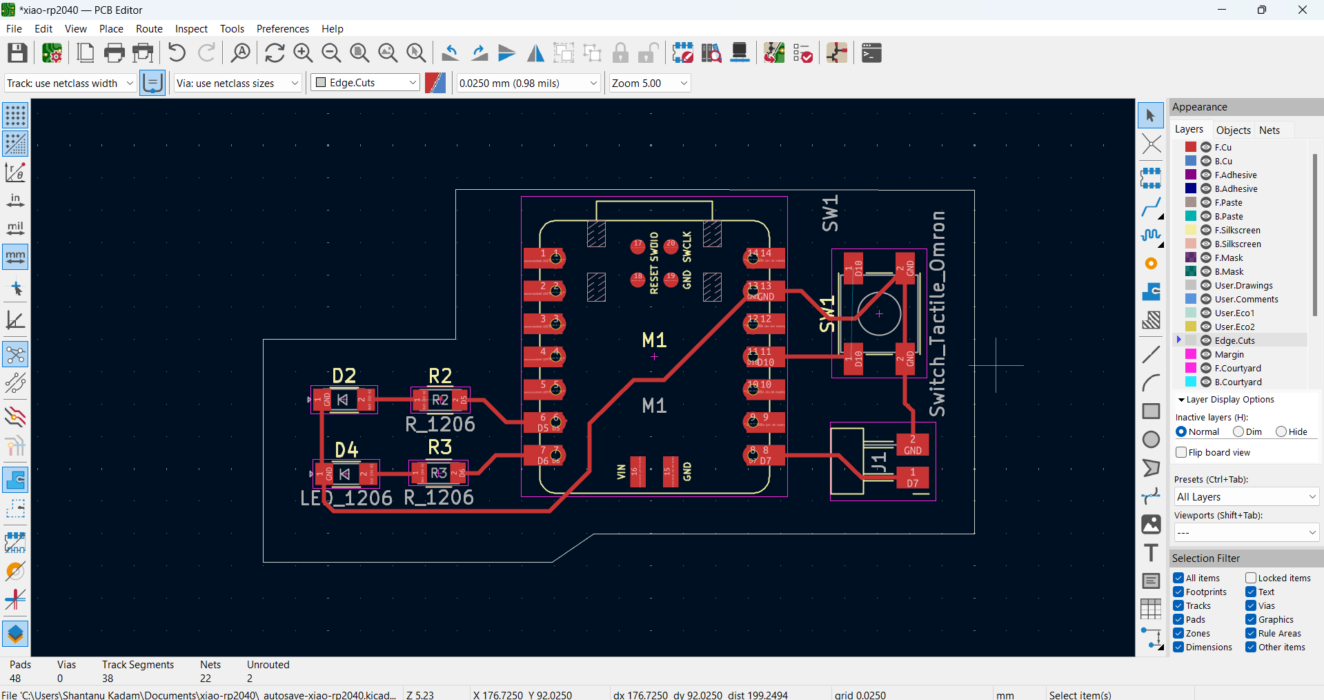
Then, I opened the PCB editor and used the "Route Track" command to make the necessary connections, ensuring that the PCB functions properly.
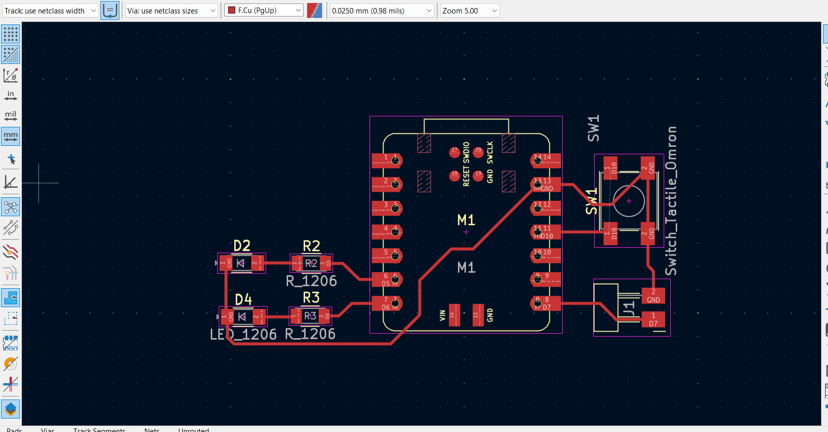
Then, I used the Edge Cuts layer, selected the Draw Line tool, and created the PCB outline.
In the next step, the file needs to be saved for PCB fabrication. The files are saved in two ways: one for traces and another for the outline cut.
To save the file for traces:
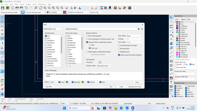
1. Go to the File menu and select Plot.
2. In the Plot window, choose SVG as the output format.
3. Select F.Cu (the front copper layer).
4. The output message will display the save location of the file.
5. Finally, click Save to store the file.
The same procedure is repeated for the edge cut, except instead of selecting F.Cu, choose Edge Cuts.
1. Go to the File menu and select Plot.
2. In the Plot window, choose SVG as the output format.
3. Select Edge Cuts instead of F.Cu.
4. Click Plot to generate the path for saving.
5. Finally, click Save to store the file.

All the aspects related to the schematic and PCB editors are not explained in detail here.
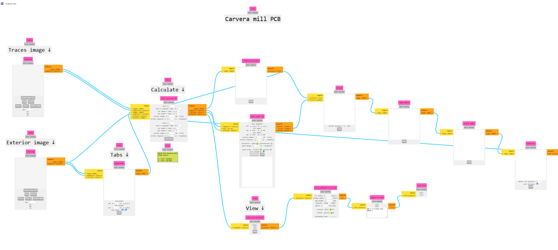
Generate Toolpath for PCB Milling
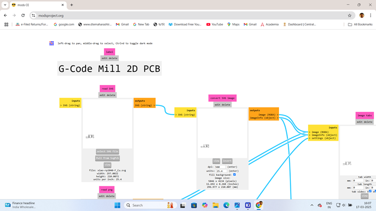
To generate the toolpath for CNC milling and create the PCB, I used the Mods Project online platform.
1. Open the Mods Project website.
2. Once the website loads, the main window appears.
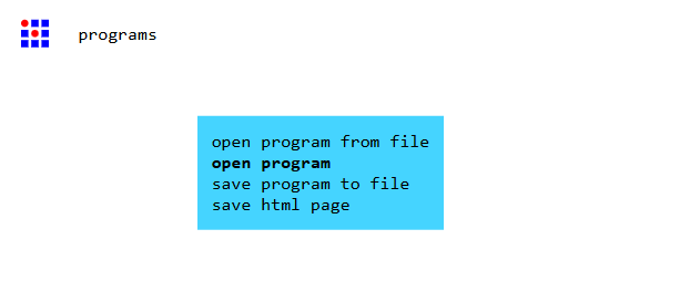
3. Then right click and from the available options, select program.
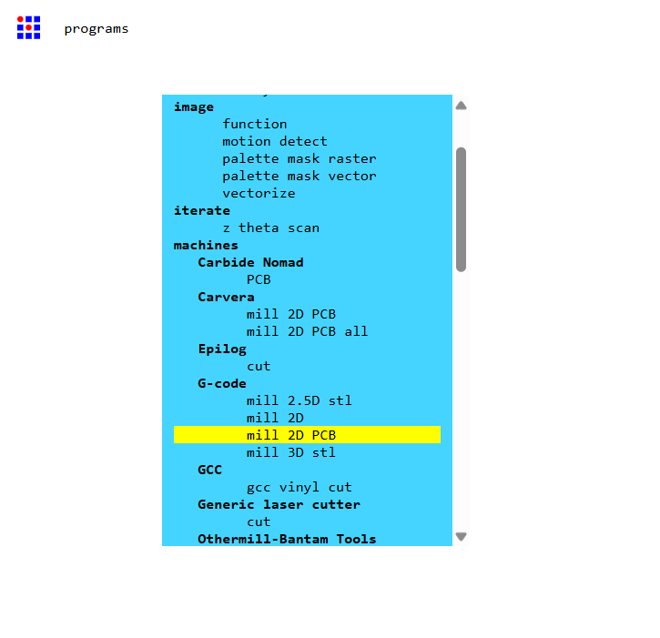
As the program opens, I scroll down and, under the G-code section, select Mill 2D PCB.
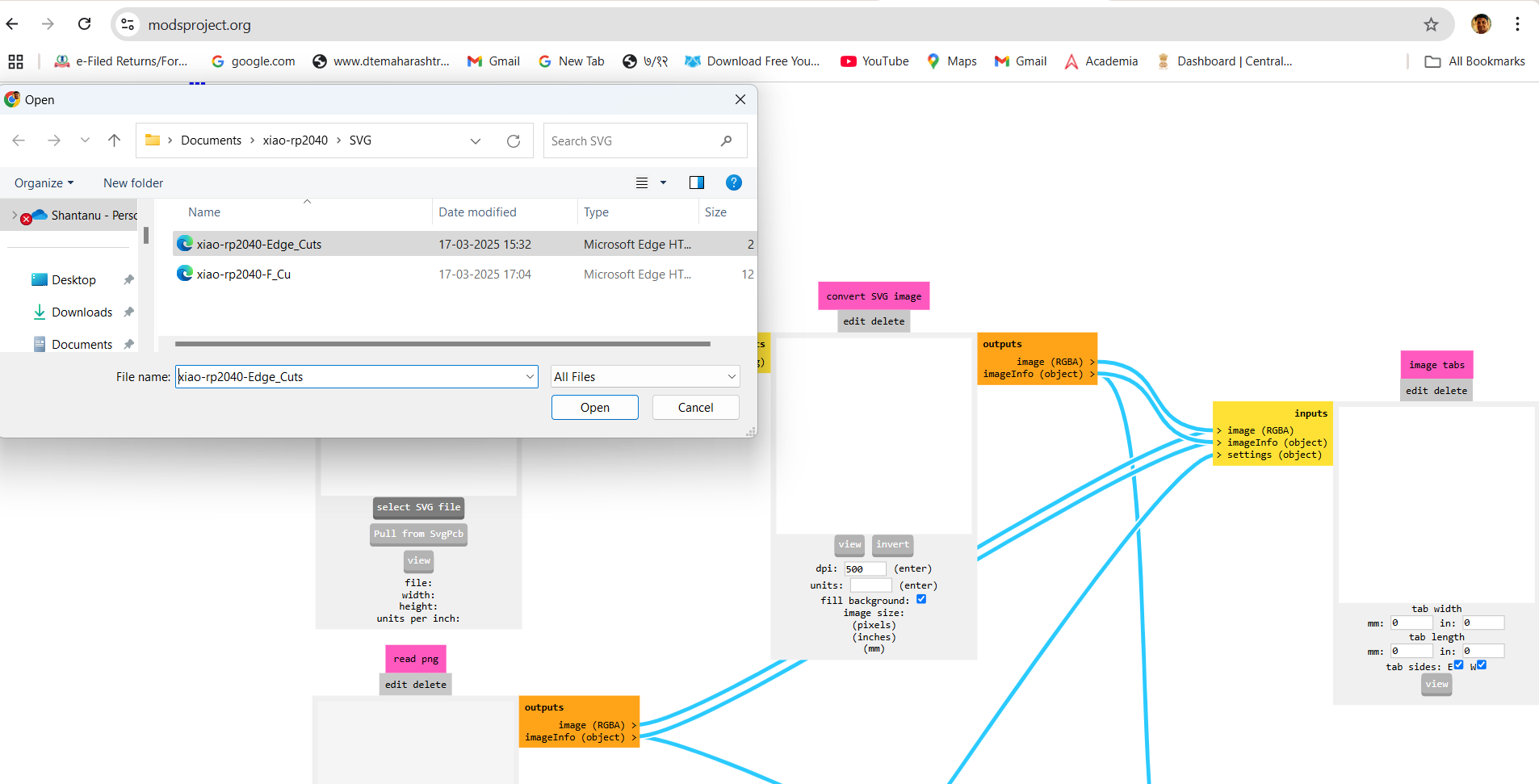
Then, go to Read SVG and select the SVG file. Then go to desired location and select .svg file format those are saved in KICAD software.
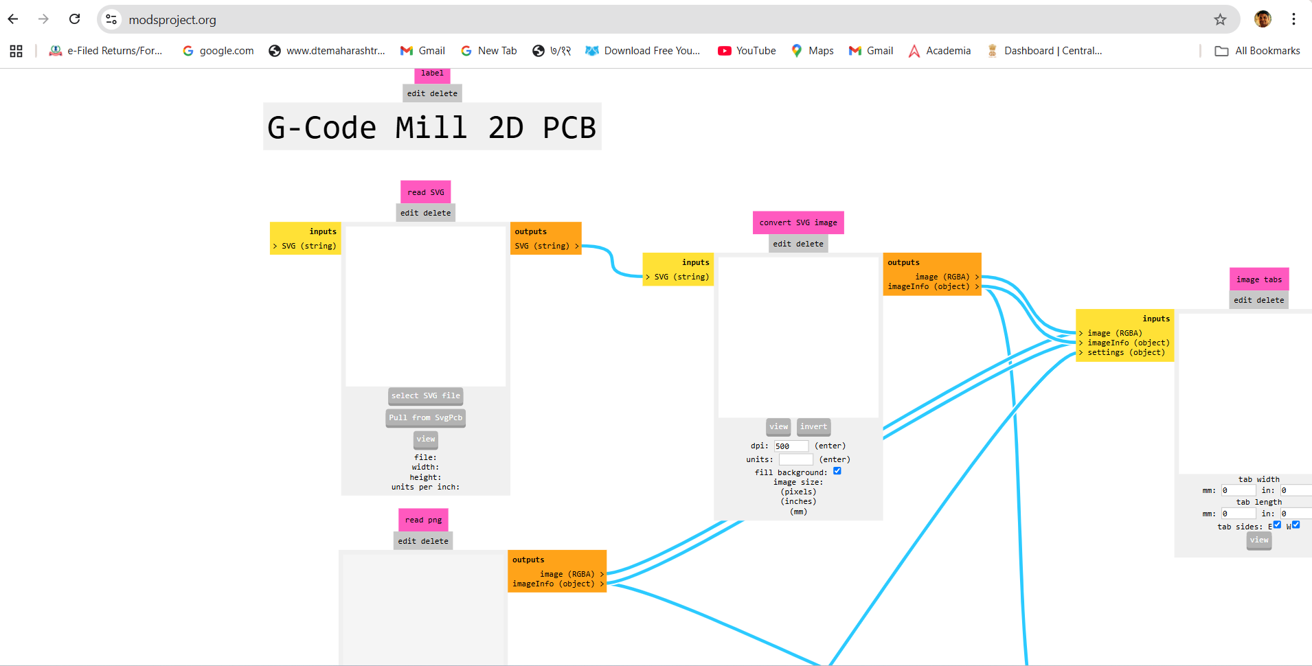
After selecting the file, press View to preview it.
Then, the preview appears in the Select SVG menu.
Then, go to Set PCB Default and select Isolate Traces.

No changes are made in the Isolate Traces settings.
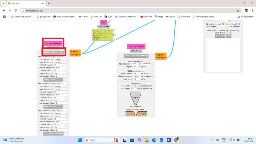
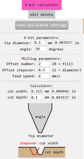
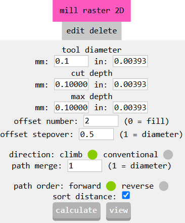
It looks like you're configuring the V-bit parameters for your CNC machining.
Open the V-bit Calculator in your software.
Set the parameters:
1. Tip Diameter: 0.1 mm
2. Angle: 30°
3. Cut Depth: 0.1 mm
4. Click on "Send Calculated Setting"
Then goes into mill raster 2d option. Change the Tool Diameter to 0.1 mm.
Then click on the view option.
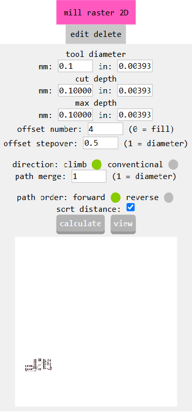
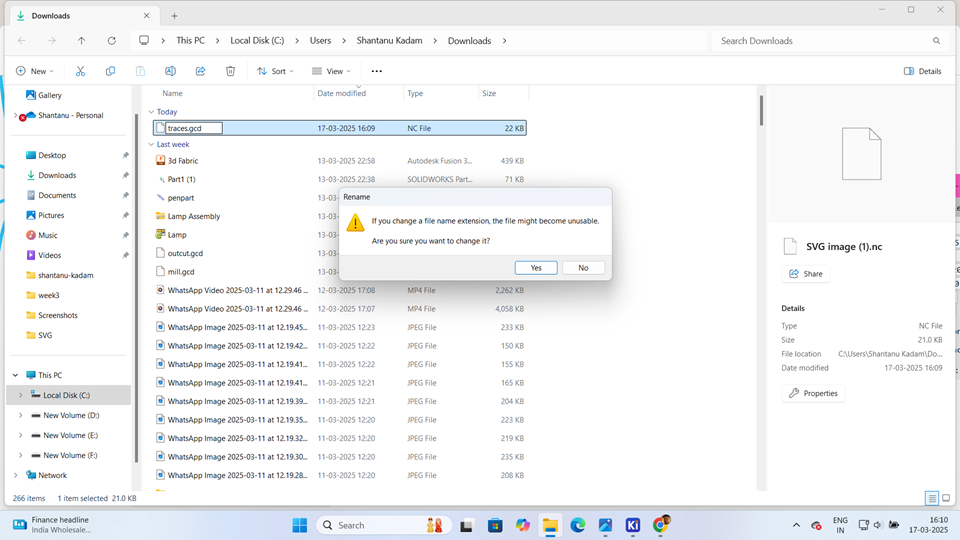
Click on the Calculate Button to generate the toolpath.The software will then generate the PCB milling file in .nc format.file is save in Downloads.Go to the "Downloads" folder and open the file. This file shows the toolpath.

After that click on the calculate option it will generate the pcb milling file in . nc format.
Navigate to the Downloads folder and locate the generated .nc file. Rename the file by changing its extension from .nc to .gcd.
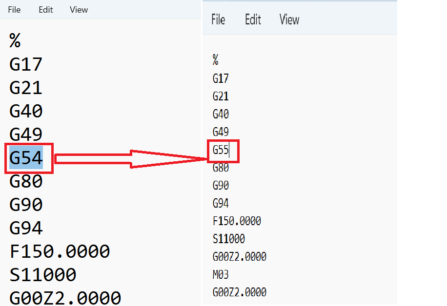
Once the file is saved in the .gcd format, open it using Notepad or a similar text editor. Locate the code G54 and replace it with G55 to adjust the work coordinate system for the PCB milling process. After making the modification, save the file and exit the editor.
Next, access the Mods CE online software to generate the outline toolpath for the PCB milling process.
Then, go to Read SVG again, and in this menu, select the SVG file.
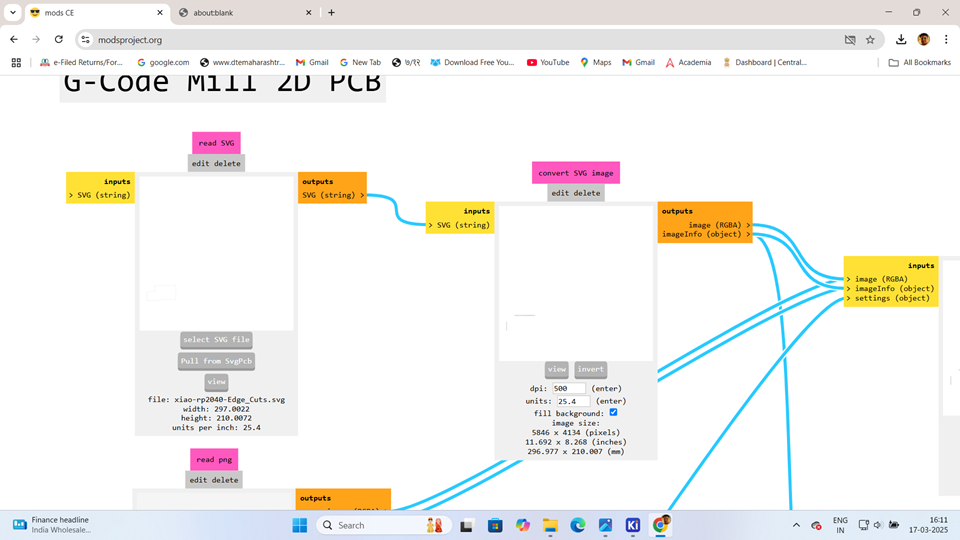
Then, go to Read SVG and select the SVG file. Then go to desired location and select .svg file format those are saved in KICAD software. Then select the edge_cut file and select open.
Then, go to Set PCB Default and select millout line (1/32).
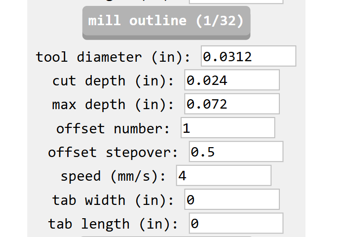
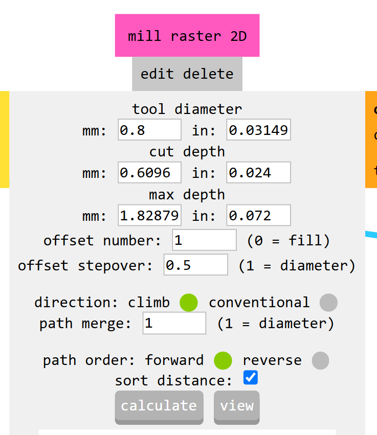
Without making any changes, go to Mill Raster 2D, change the tool diameter to 0.8mm, and save the changes.
After that click on the calculate option it will generate the pcb milling file in . nc format.
Navigate to the Downloads folder and locate the generated .nc file. Rename the file by changing its extension from .nc to .gcd.
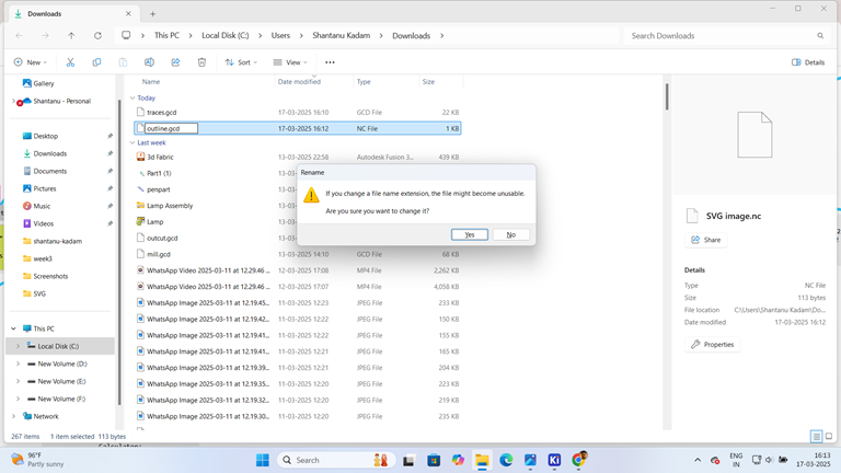
Once the file is saved in the .gcd format, open it using Notepad or a similar text editor. Locate the code G54 and replace it with G55 to adjust the work coordinate system for the PCB milling process. After making the modification, save the file and exit the editor.
CNC Milling Process
Once the trace and outline files are generated, the PCB design is ready for manufacturing.
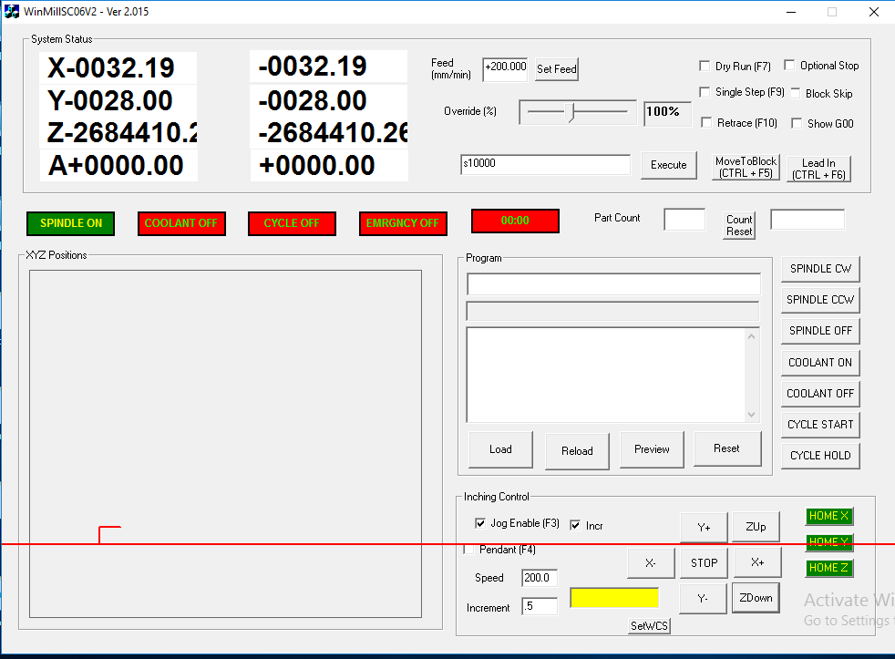
Then, proceed to the PCB milling machine, where the machine software is launched. Initially, the startup window is displayed.

Next, it is important to set the origin point. To do this, first, click on the "Jog Enable" menu, then select "Incremental." Set the desired increment value, and use the -X, +X, -Y, +Y, Z-up, and Z-down controls to position the spindle accurately.
When go into the Set WCS menu and set X0, Y0, Z0, you are likely defining a new origin point for design.
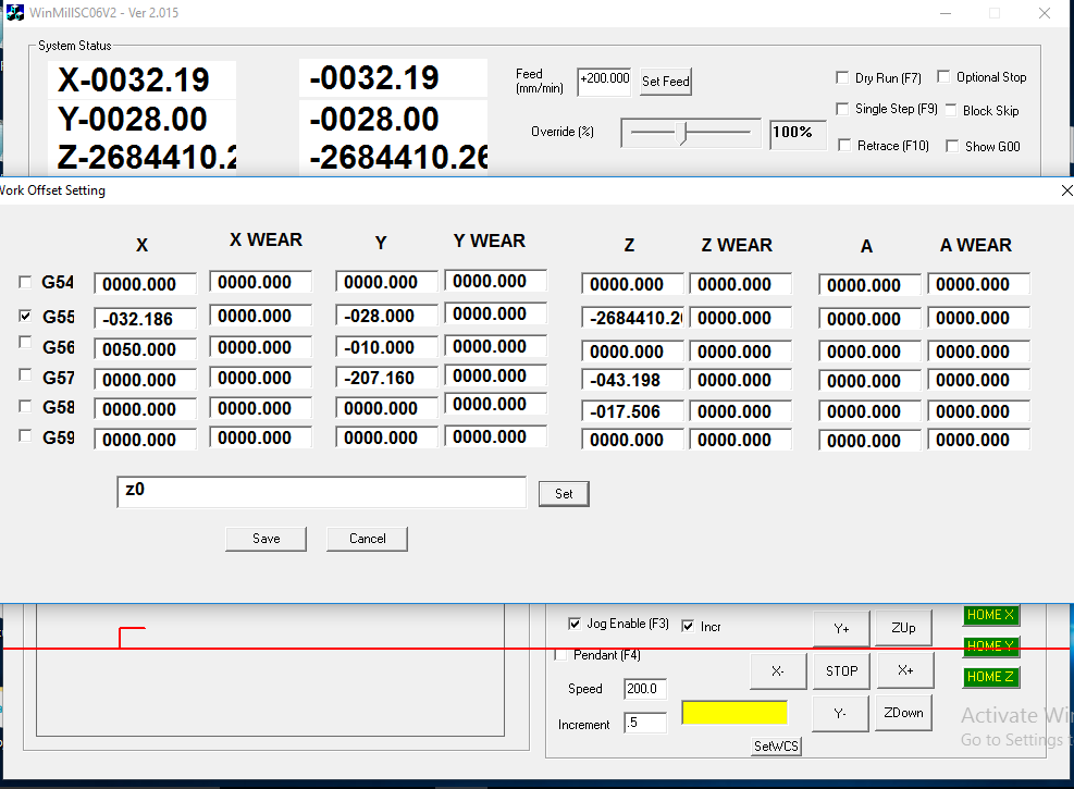
Then, click the Save button to set the origin for the PCB milling process. The screen will display the coordinates X0, Y0, Z0, confirming that the new reference point has been established.
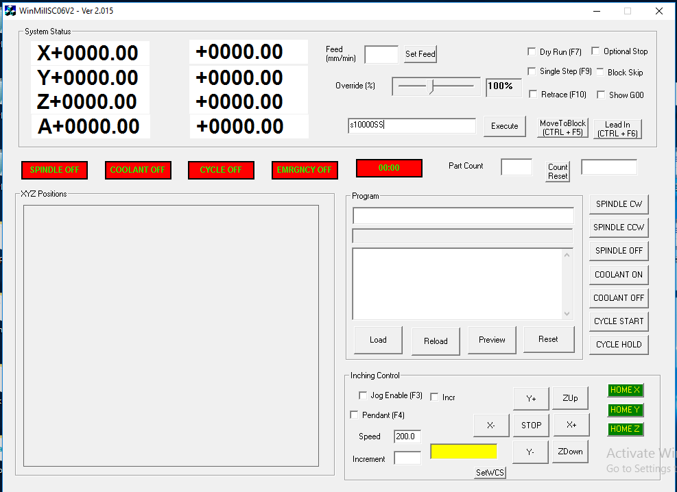
Next, navigate to the Increments setting, configure it as needed, and click Z-Up to move the tool upward.
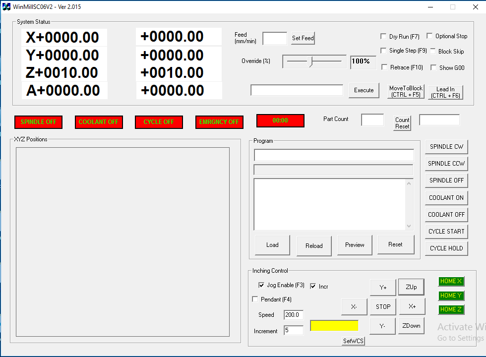
Then, navigate to the Load menu and select the program from the desired location.
Load the traces program to initiate the cutting process for the PCB traces.
Then, click Cycle Start to begin the milling process.
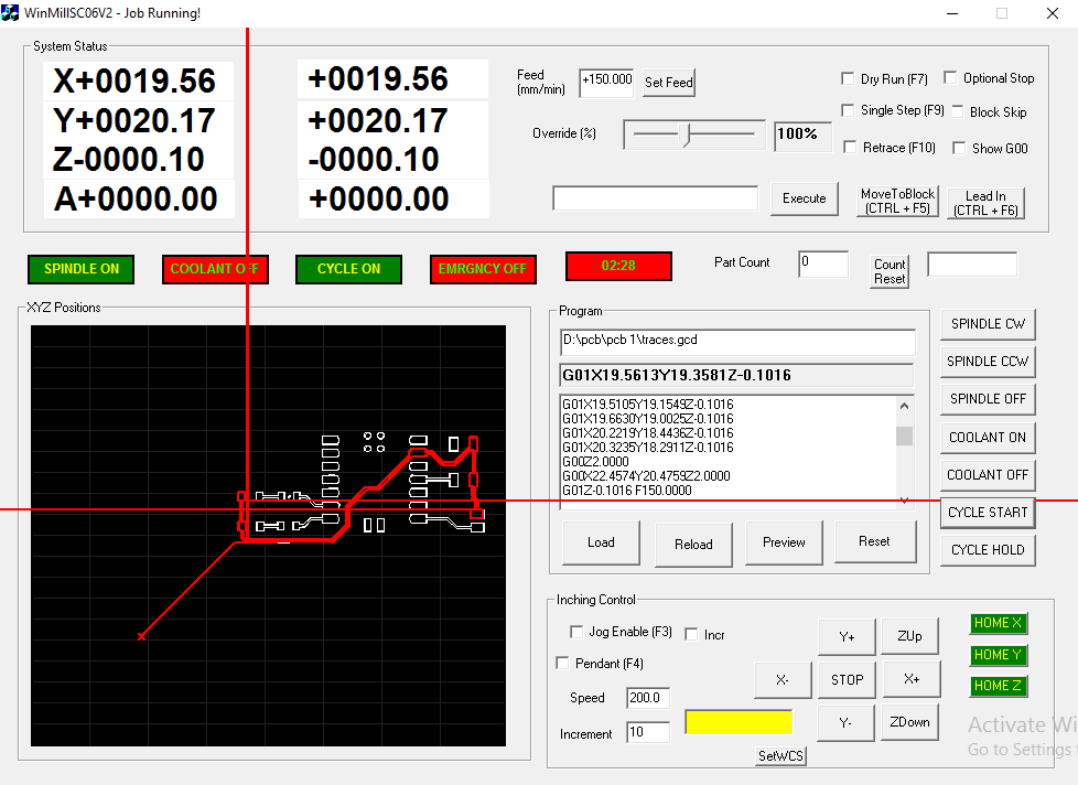
As the milling process begins, the tool rotates at a speed of 10,000 RPM, as specified in the program, and starts cutting the PCB traces.
Once the traces are cut, the program is completed. Next, change the tool from a V-bit to a 0.8mm drilling tool. Then, following the same procedure, load the edge cut program while maintaining the previously set origin and click Cycle Start to begin the process.
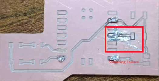
Once the edge cut program cycle is completed, the PCB is ready for the soldering process.
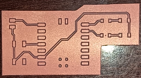
PCB soldering
With the PCB milling process completed, the board is now ready for soldering. In the next step, the soldering process will be carried out.
In the soldering process, I connected the push button, resistor, LED, connector, and XIAO RP2040 board to the PCB.
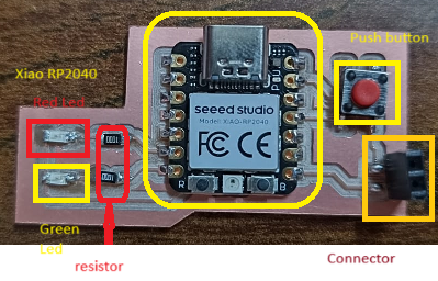
Soldering on the PCB is a challenging process for me. While soldering, the solder metal tends to spread to adjacent pins, causing unintended connections and leading to PCB failure.
Hero Shot
PCB Output
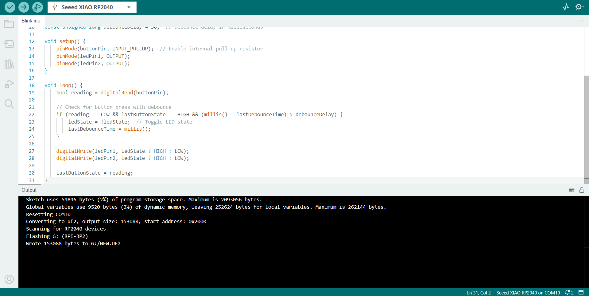
As the PCB is ready, the next step is writing a program for LED blinking. Initially, both LEDs will blink simultaneously. For this, I am writing the program using the Arduino IDE.
Connections
Push Button- D10
LED 1 (First)- D6
LED 2 (Second)- D5
GND (Common)- GND
Programe Code
const int buttonPin = D10; // Push button pin
const int ledPin1 = D6; // First LED pin
const int ledPin2 = D5; // Second LED pin
bool ledState = false; // Track LED state
bool lastButtonState = HIGH;
bool currentButtonState;
unsigned long lastDebounceTime = 0;
const unsigned long debounceDelay = 50; // Debounce delay in milliseconds
void setup() {
pinMode(buttonPin, INPUT_PULLUP); // Enable internal pull-up resistor
pinMode(ledPin1, OUTPUT);
pinMode(ledPin2, OUTPUT);
}
void loop() {
bool reading = digitalRead(buttonPin);
// Check for button press with debounce
if (reading == LOW && lastButtonState == HIGH && (millis() - lastDebounceTime) > debounceDelay) {
ledState = !ledState; // Toggle LED state
lastDebounceTime = millis();
}
digitalWrite(ledPin1, ledState ? HIGH : LOW);
digitalWrite(ledPin2, ledState ? HIGH : LOW);
lastButtonState = reading;
}
Then uploading it to the XIAO RP2040.
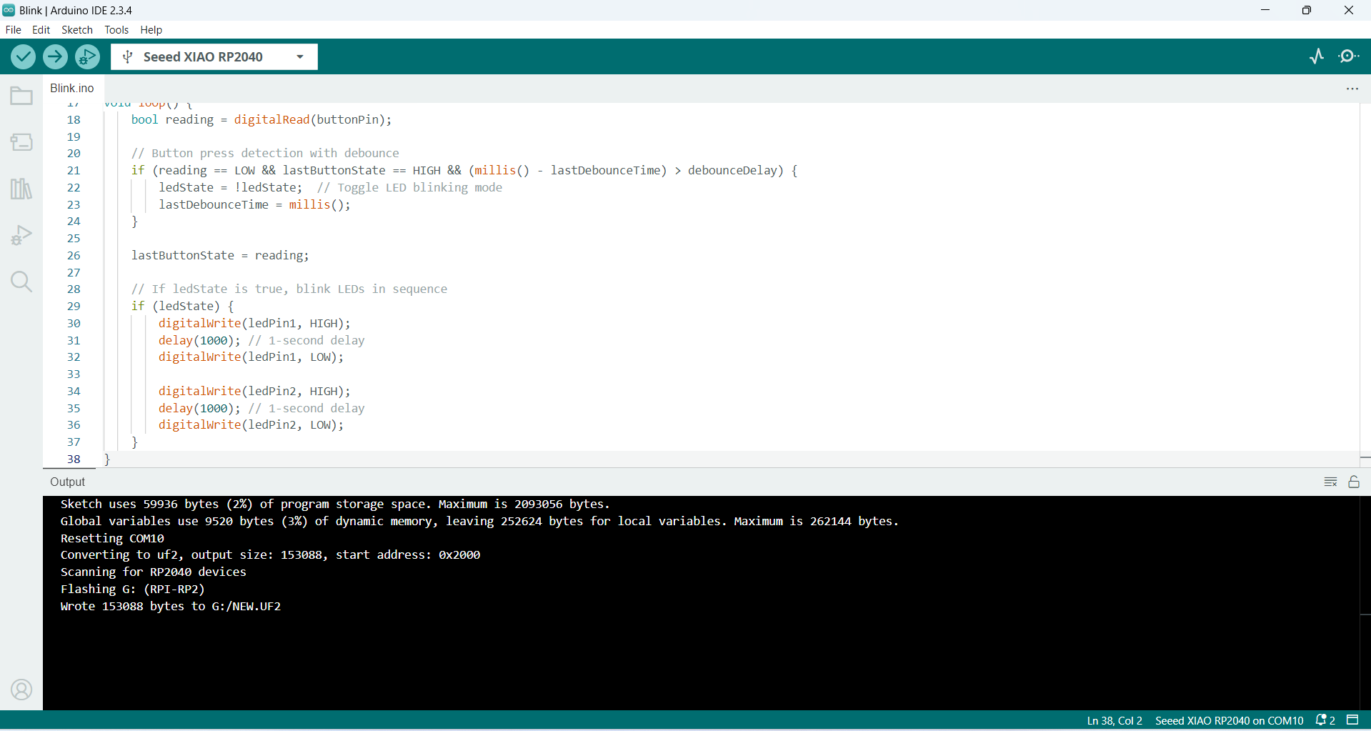
Write a second program to make the LEDs blink one after another, each for 1 second.
const int buttonPin = D10; // Push button pin
const int ledPin1 = D6; // First LED pin
const int ledPin2 = D5; // Second LED pin
bool ledState = false; // Track LED state (ON/OFF mode)
bool lastButtonState = HIGH;
unsigned long lastDebounceTime = 0;
const unsigned long debounceDelay = 50; // Debounce delay in milliseconds
void setup() {
pinMode(buttonPin, INPUT_PULLUP); // Internal pull-up resistor
pinMode(ledPin1, OUTPUT);
pinMode(ledPin2, OUTPUT);
}
void loop() {
bool reading = digitalRead(buttonPin);
// Button press detection with debounce
if (reading == LOW && lastButtonState == HIGH && (millis() - lastDebounceTime) > debounceDelay) {
ledState = !ledState; // Toggle LED blinking mode
lastDebounceTime = millis();
}
lastButtonState = reading;
// If ledState is true, blink LEDs in sequence
if (ledState) {
digitalWrite(ledPin1, HIGH);
delay(1000); // 1-second delay
digitalWrite(ledPin1, LOW);
digitalWrite(ledPin2, HIGH);
delay(1000); // 1-second delay
digitalWrite(ledPin2, LOW);
}
}
Then uploading it to the XIAO RP2040.
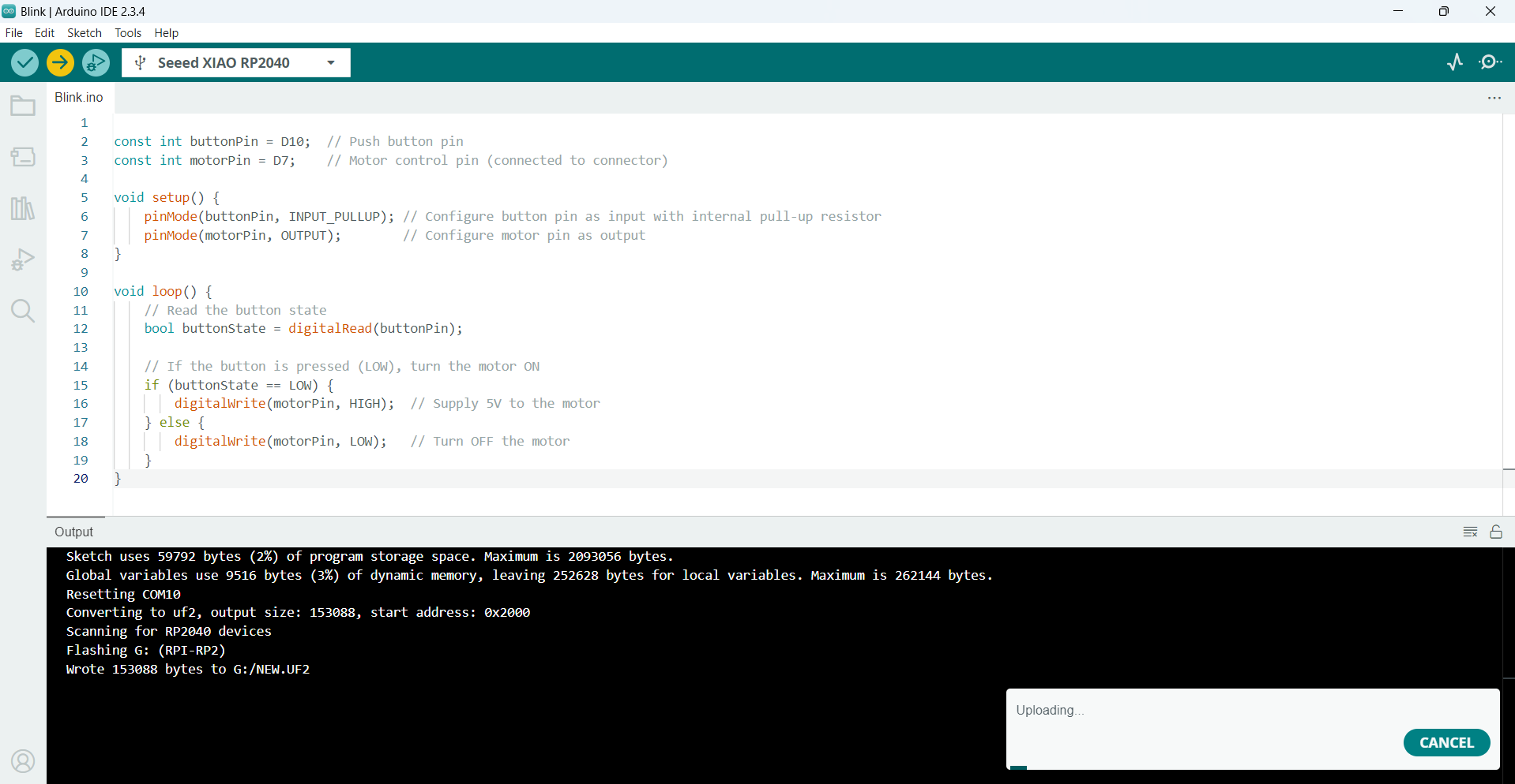
Here is the third program to control a 5V motor using a connector on pin D7 of the XIAO RP2040.
const int buttonPin = D10; // Push button pin
const int motorPin = D7; // Motor control pin (connected to connector)
void setup() {
pinMode(buttonPin, INPUT_PULLUP); // Configure button pin as input with internal pull-up resistor
pinMode(motorPin, OUTPUT); // Configure motor pin as output}
void loop() {
// Read the button state
bool buttonState = digitalRead(buttonPin);
// If the button is pressed (LOW), turn the motor ON
if (buttonState == LOW) {
} else {
digitalWrite(motorPin, LOW); // Turn OFF the motor
}
}
Then uploading it to the XIAO RP2040.