Week 10
Output Devices
This week, I explored the integration of output devices with PCBs, a crucial aspect of embedded systems and electronics design. Output devices such as LEDs, buzzers, motors, and displays serve as interfaces between the microcontroller and the physical world, enabling interaction and feedback. Understanding how to connect, control, and optimize these devices is essential for designing efficient and functional circuits.
I focused on selecting appropriate output components based on power requirements, communication protocols, and control mechanisms. Additionally, I examined driver circuits, power management strategies, and programming techniques to interface these devices with microcontrollers like the ESP32-C3. Through hands-on experimentation, I gained insights into troubleshooting common issues and optimizing performance for real-world applications.
This week, I focused on two assignments—one as part of a group with Dr. Sujit and another as an individual assignments. The group assignment involved collaborative learning and practical implementation, while the individual assignment allowed me to apply my skills independently.
Group Assignment
Individual Assignment
Group Assignment
As part of our group assignment, Dr. Sujit and I analyzed the output devices of the PCB, which include indicators such as LEDs, displays, and relays that facilitate communication between the system and the user.
The group assignment is linked here
Individual Assignment
This week, I focused on designing a PCB for output devices as part of my individual assignment. The goal was to create a functional circuit that could interface with an ESP32-C3 microcontroller to control various output components. After designing the PCB using an EDA tool, I proceeded with milling the board to bring the design to life.
Once the PCB was fabricated, I programmed the ESP32-C3 to control the connected output devices and observed their behavior. This process involved understanding circuit design principles, ensuring proper connections, and debugging any issues that arose during testing. Through this hands-on approach, I gained valuable experience in designing, fabricating, and testing PCBs for embedded systems applications.
Design of PCB with KICAD software
As I explained in Week Six, I learned to use this software for PCB design. It is open-source and easily available online. Using this software, I designed a simple PCB for output devices.
The schematic diagram explains that I used the ESP32-C3 board for the PCB design. Additionally, I included an LED and a Four connector. In that four pin connector, Three pin connector and Two pin connector Using all these components, I designed a PCB for this week.
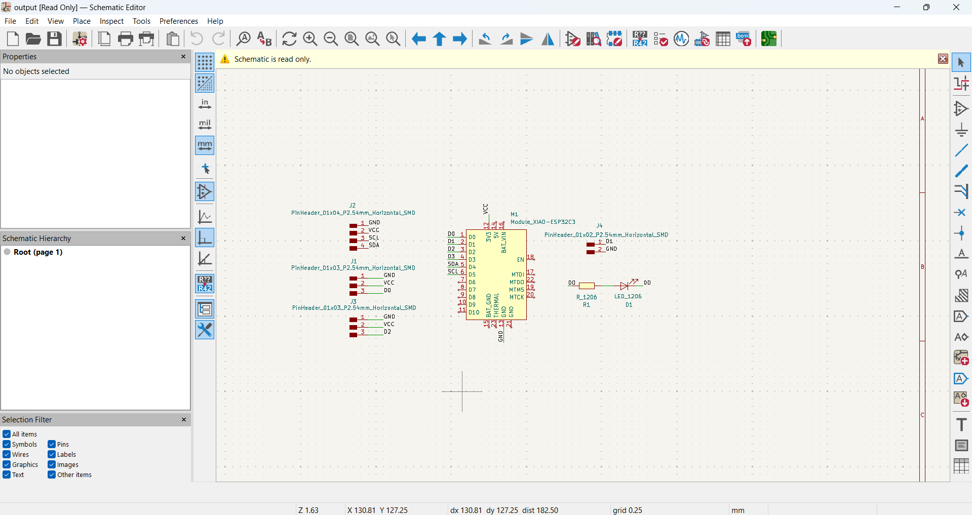
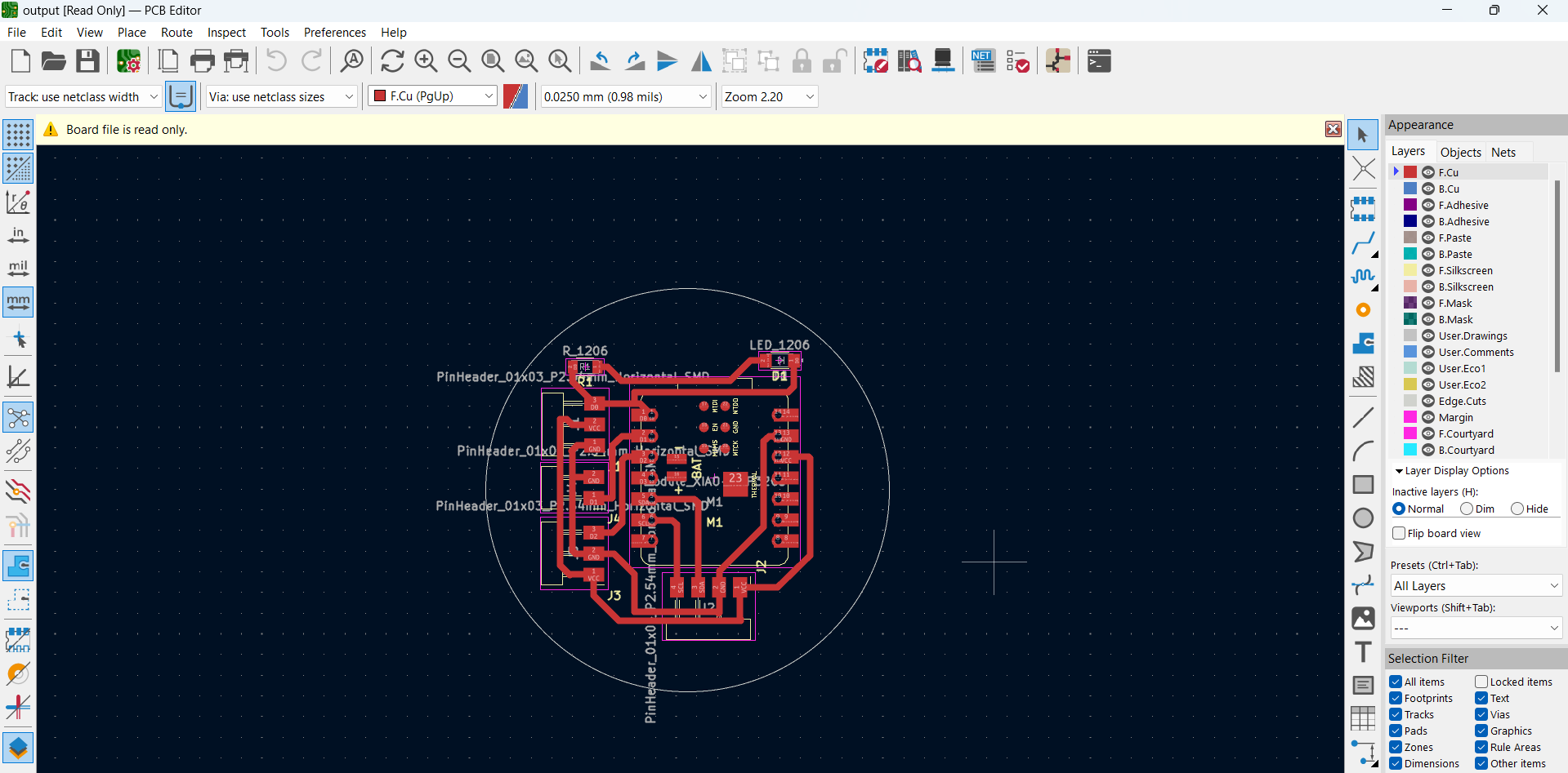
Then, I opened the PCB editor and used the "Route Track" command to make the necessary connections, ensuring that the PCB functions properly.
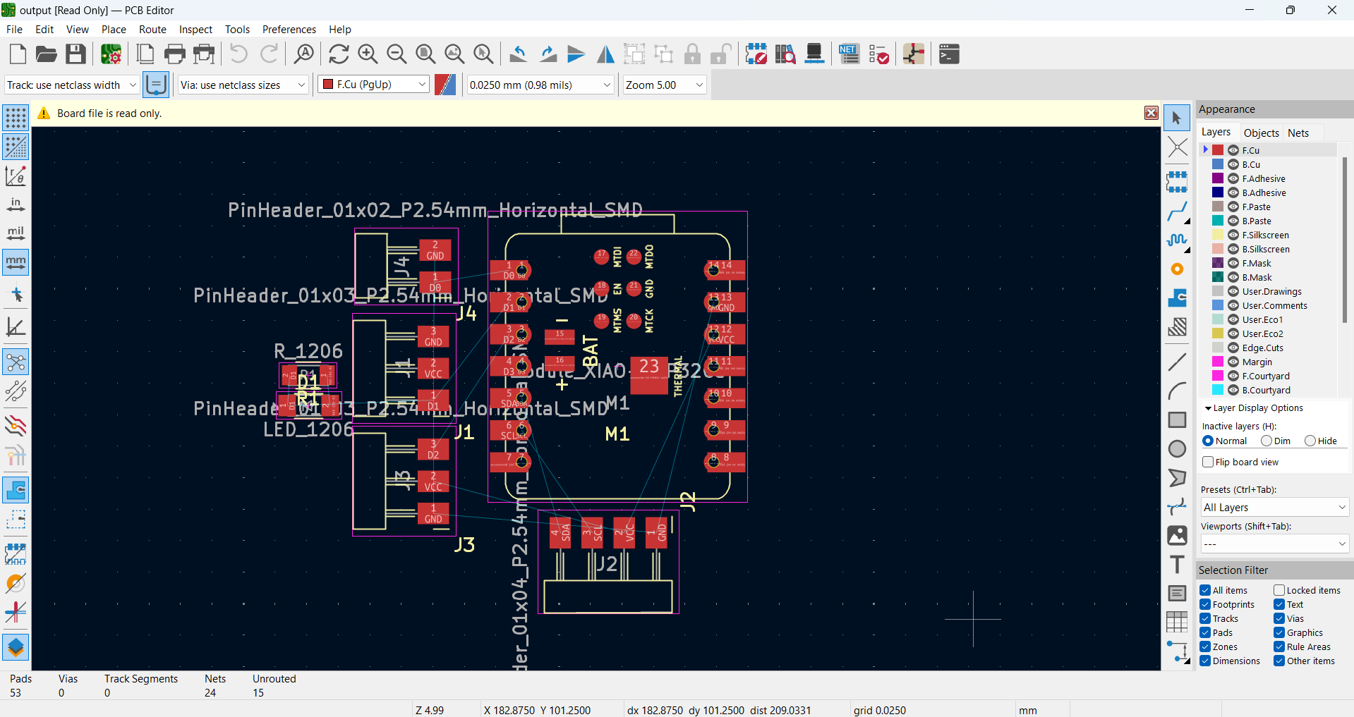
Then, using the Route Track command, I established proper connections on the PCB, ensuring a well-structured and functional circuit layout. Then, I used the Edge Cuts layer, selected the Draw Line tool, and created the PCB outline.
In the next step, the file needs to be saved for PCB fabrication. The files are saved in two ways: one for traces and another for the outline cut.
To save the file for traces:
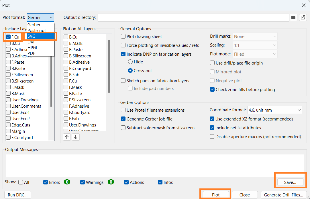
1. Go to the File menu and select Plot.
2. In the Plot window, choose SVG as the output format.
3. Select F.Cu (the front copper layer).
4. The output message will display the save location of the file.
5. Finally, click Save to store the file.
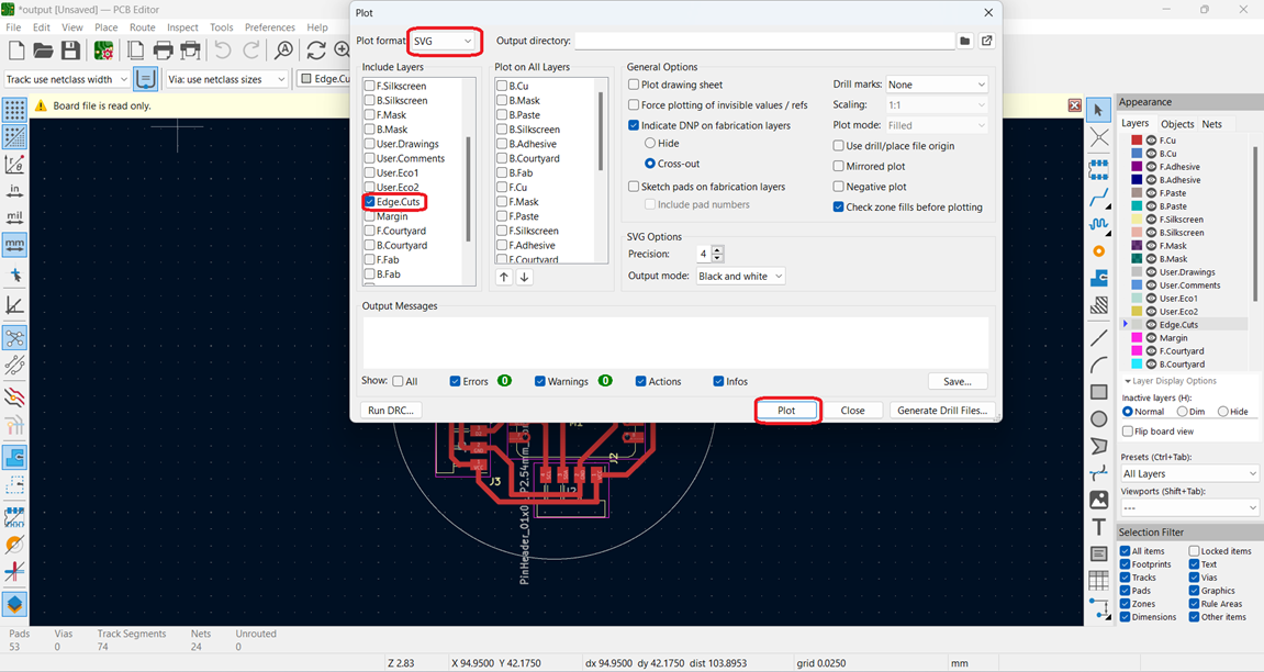
The same procedure is repeated for the edge cut, except instead of selecting F.Cu, choose Edge Cuts.
1. Go to the File menu and select Plot.
2. In the Plot window, choose SVG as the output format.
3. Select Edge Cuts instead of F.Cu.
4. Click Plot to generate the path for saving.
5. Finally, click Save to store the file.
All the aspects related to the schematic and PCB editors are not explained in detail here.
Generate Toolpath for PCB Milling
To generate the toolpath for CNC milling and create the PCB, I used the Mods Project online platform.
1. Open the Mods Project website.
2. Once the website loads, the main window appears.
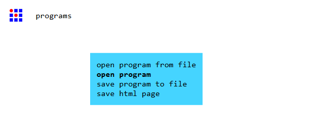
3. Then right click and from the available options, select program.
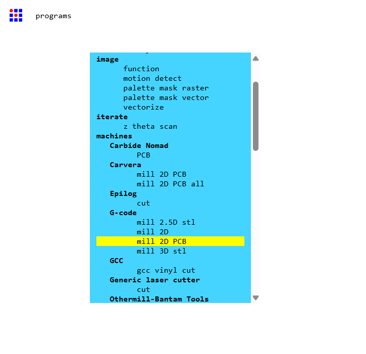
As the program opens, I scroll down and, under the G-code section, select Mill 2D PCB.
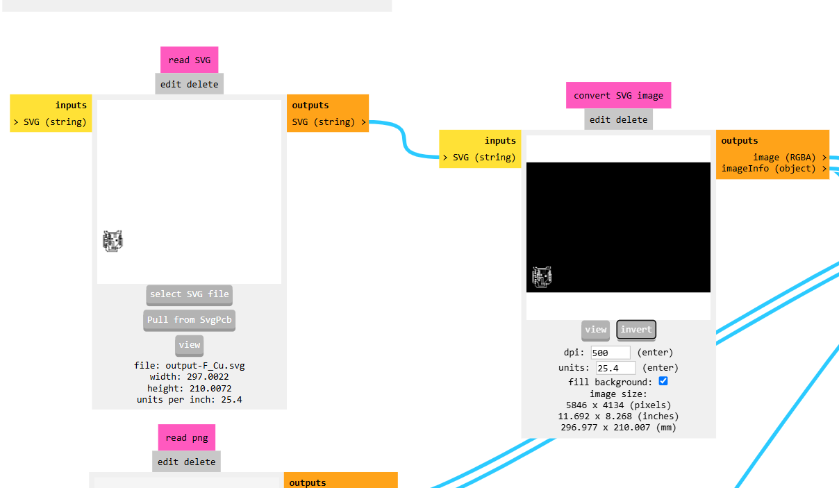
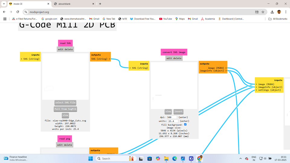
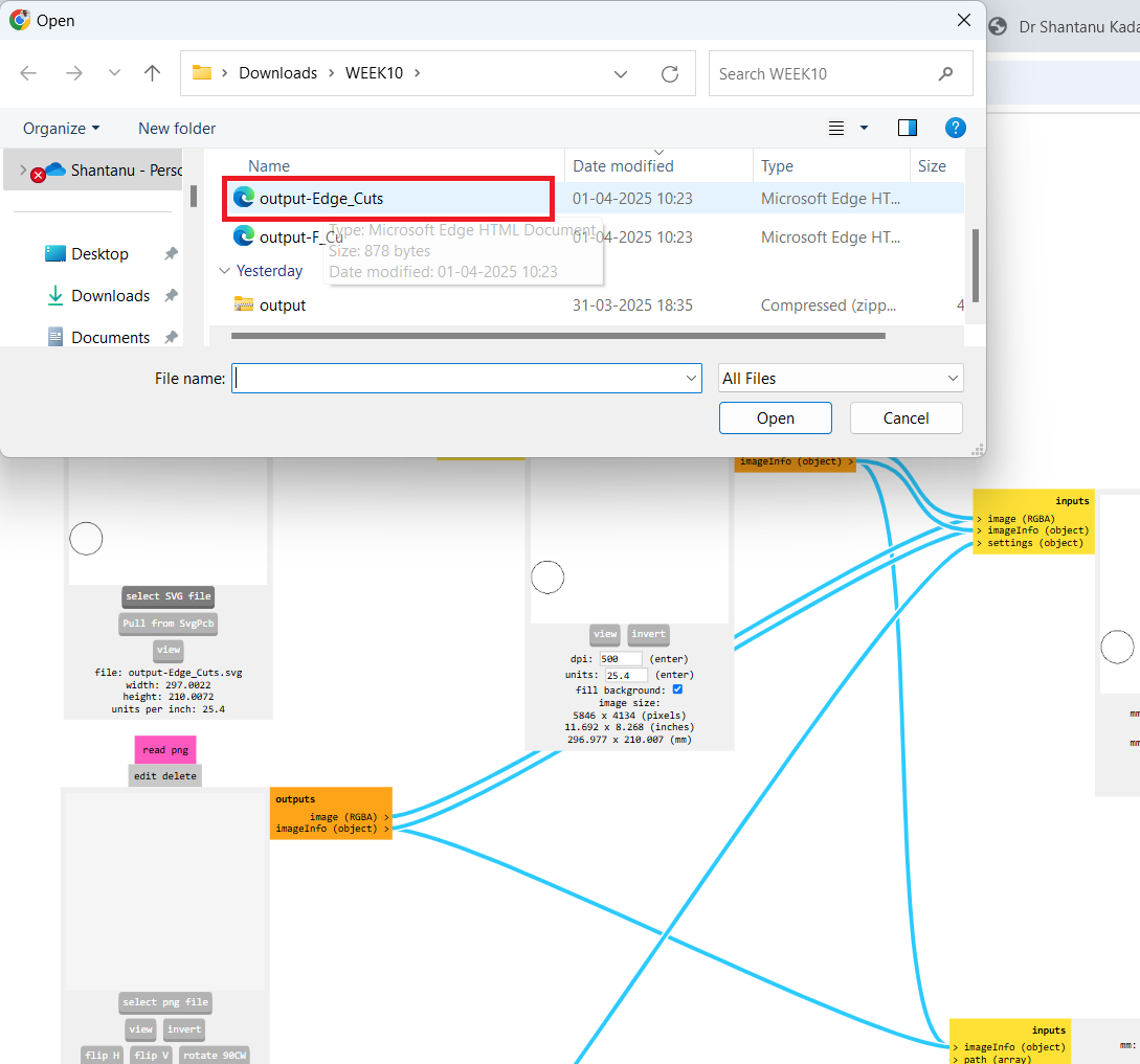
Then, go to Read SVG and select the SVG file. Then go to desired location and select .svg file format those are saved in KICAD software.
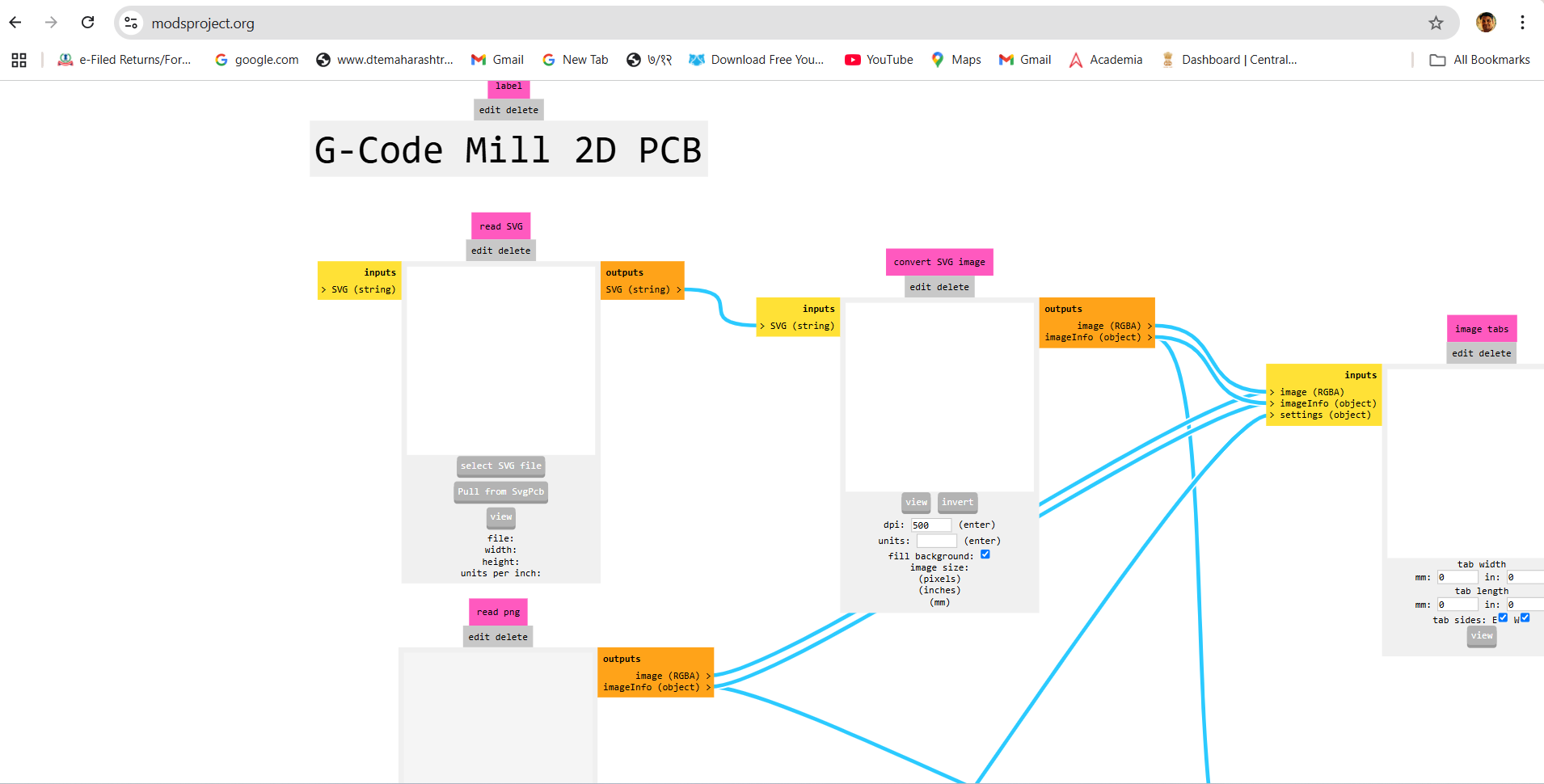
After selecting the file, press View to preview it.
Then, the preview appears in the Select SVG menu. Then, navigate to the "Convert SVG Image" section and select the "Invert" option.
Then, go to Set PCB Default and select Isolate Traces.

No changes are made in the Isolate Traces settings.
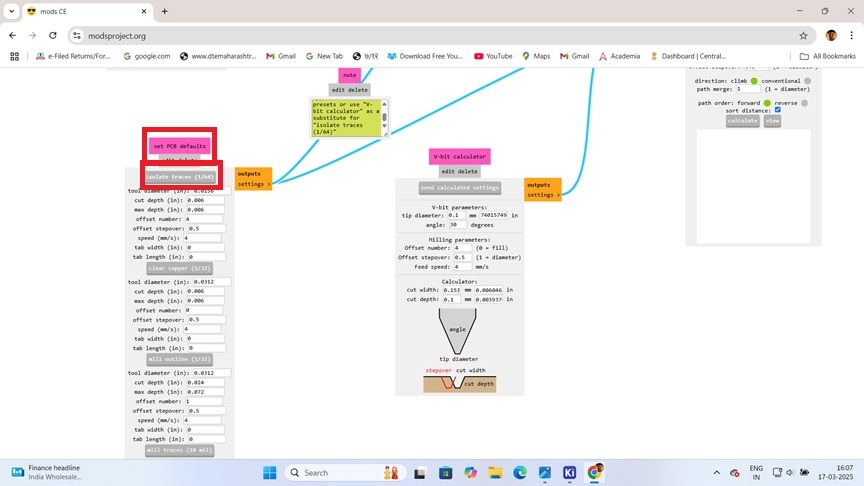
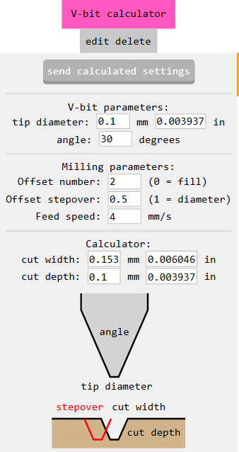
It looks like you're configuring the V-bit parameters for your CNC machining.
Open the V-bit Calculator in your software.
Set the parameters:
1. Tip Diameter: 0.1 mm
2. Angle: 30°
3. Cut Depth: 0.1 mm
4. Click on "Send Calculated Setting"
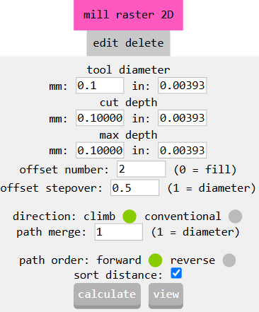
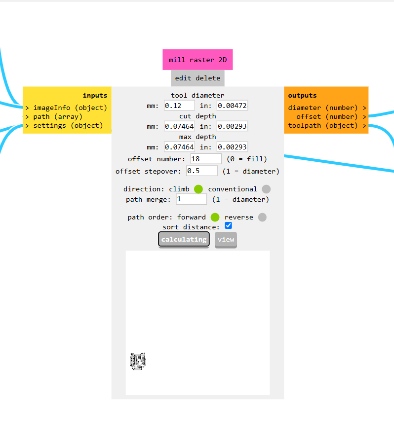
Then goes into mill raster 2d option. Change the Tool Diameter to 0.1 mm. Then, press the "Calculate" option. Once the calculation is complete, the file will be downloaded to the "Downloads" section.
Then click on the view option.
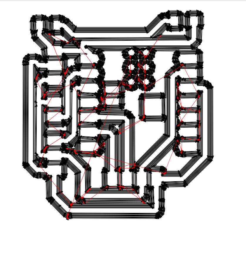
Click on the Calculate Button to generate the toolpath.The software will then generate the PCB milling file in .nc format.file is save in Downloads.Go to the "Downloads" folder and open the file. This file shows the toolpath.
After that click on the calculate option it will generate the pcb milling file in . nc format.
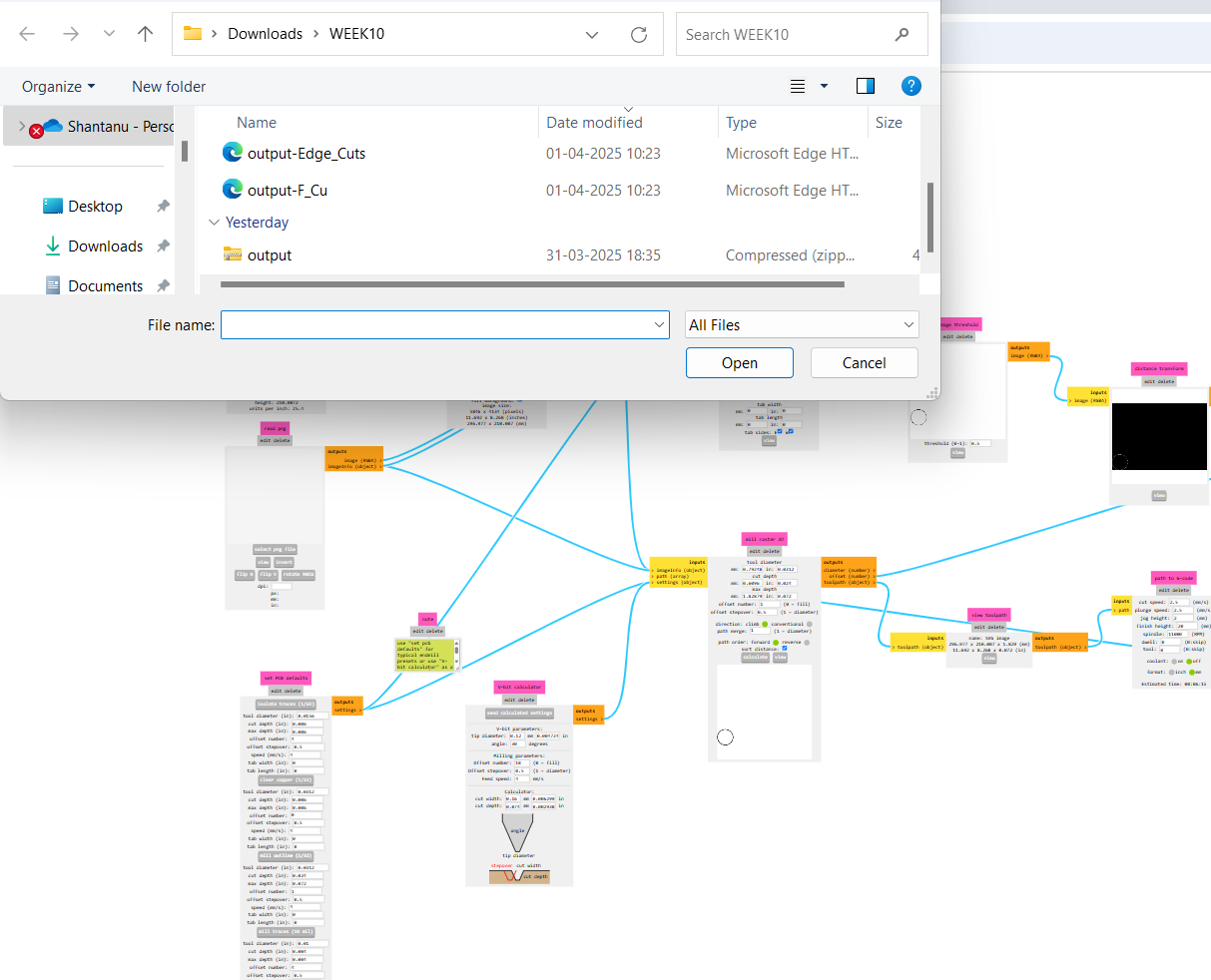
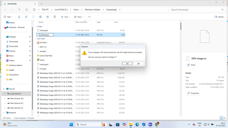
Navigate to the Downloads folder and locate the generated .nc file. Rename the file by changing its extension from .nc to .gcd.
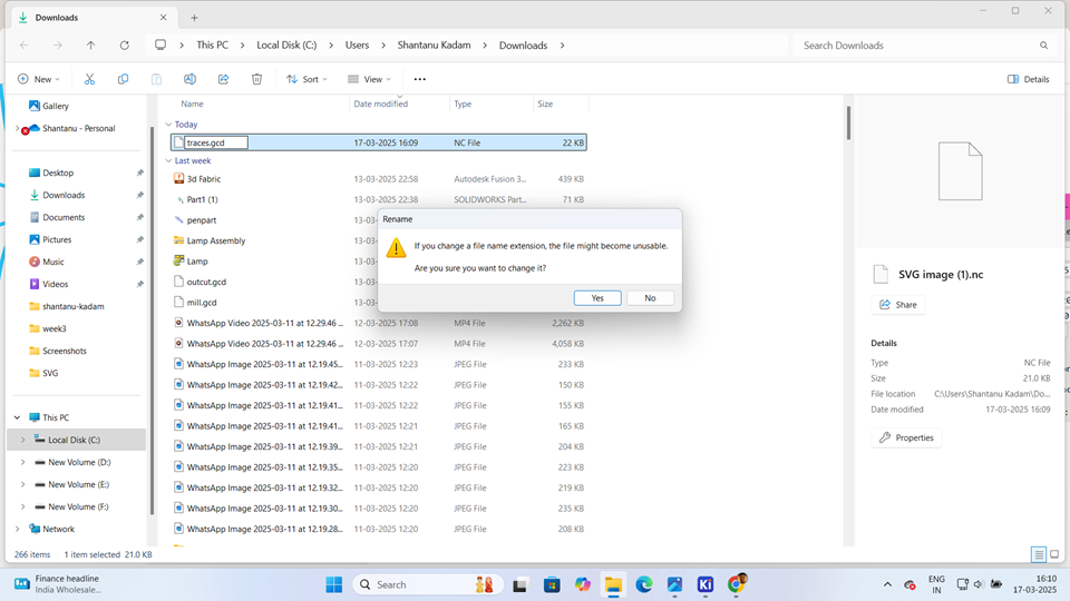
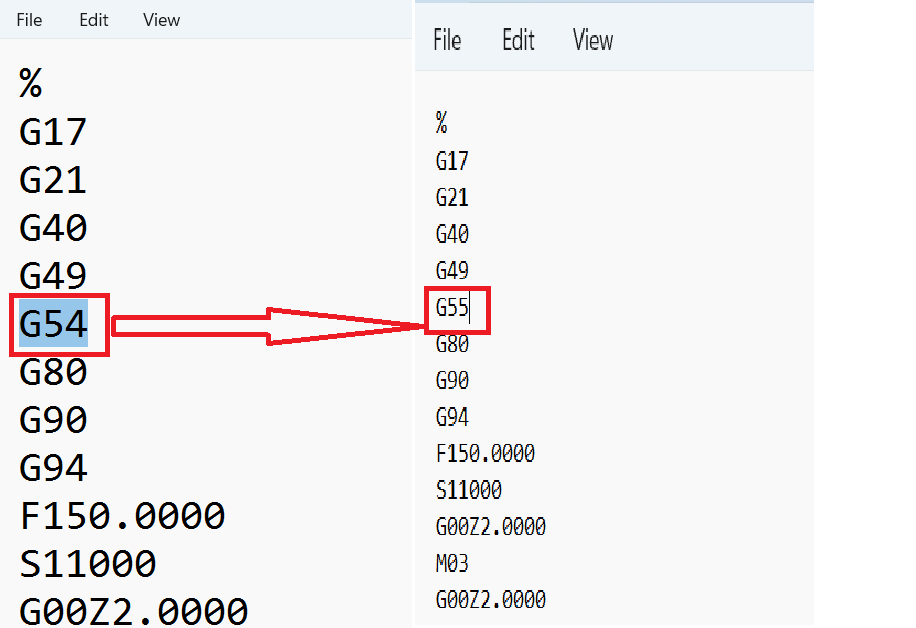
Once the file is saved in the .gcd format, open it using Notepad or a similar text editor. Locate the code G54 and replace it with G55 to adjust the work coordinate system for the PCB milling process. After making the modification, save the file and exit the editor.
Next, access the Mods CE online software to generate the outline toolpath for the PCB milling process.
Then, go to Read SVG again, and in this menu, select the SVG file.
Then, go to Read SVG and select the SVG file. Then go to desired location and select .svg file format those are saved in KICAD software. Then select the edge_cut file and select open.
Then, go to Set PCB Default and select millout line (1/32).
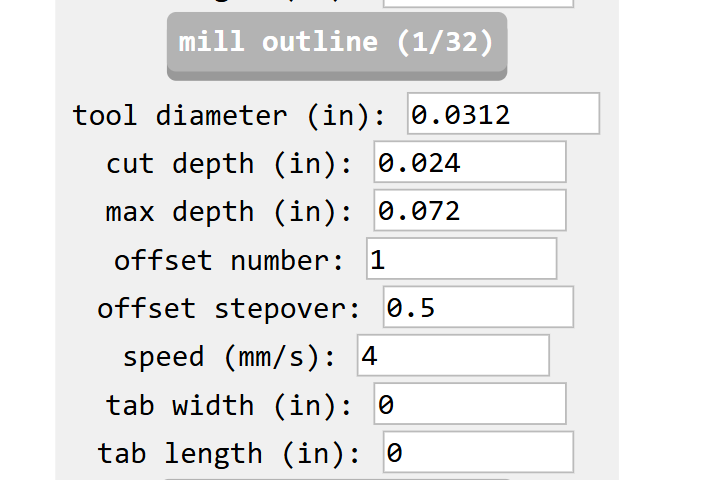
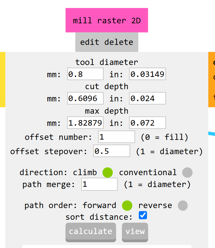
Without making any changes, go to Mill Raster 2D, change the tool diameter to 0.8mm, and save the changes.
After that click on the calculate option it will generate the pcb milling file in . nc format.
Navigate to the Downloads folder and locate the generated .nc file. Rename the file by changing its extension from .nc to .gcd.
Once the file is saved in the .gcd format, open it using Notepad or a similar text editor. Locate the code G54 and replace it with G55 to adjust the work coordinate system for the PCB milling process. After making the modification, save the file and exit the editor.
CNC Milling Process
Once the trace and outline files are generated, the PCB design is ready for manufacturing.
Then, proceed to the PCB milling machine, where the machine software is launched. Initially, the startup window is displayed.
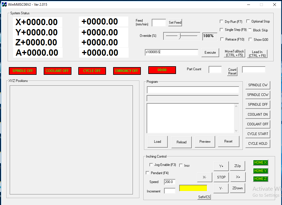
Next, it is important to set the origin point. To do this, first, click on the "Jog Enable" menu, then select "Incremental." Set the desired increment value, and use the -X, +X, -Y, +Y, Z-up, and Z-down controls to position the spindle accurately.
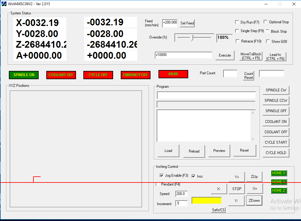
When go into the Set WCS menu and set X0, Y0, Z0, you are likely defining a new origin point for design.
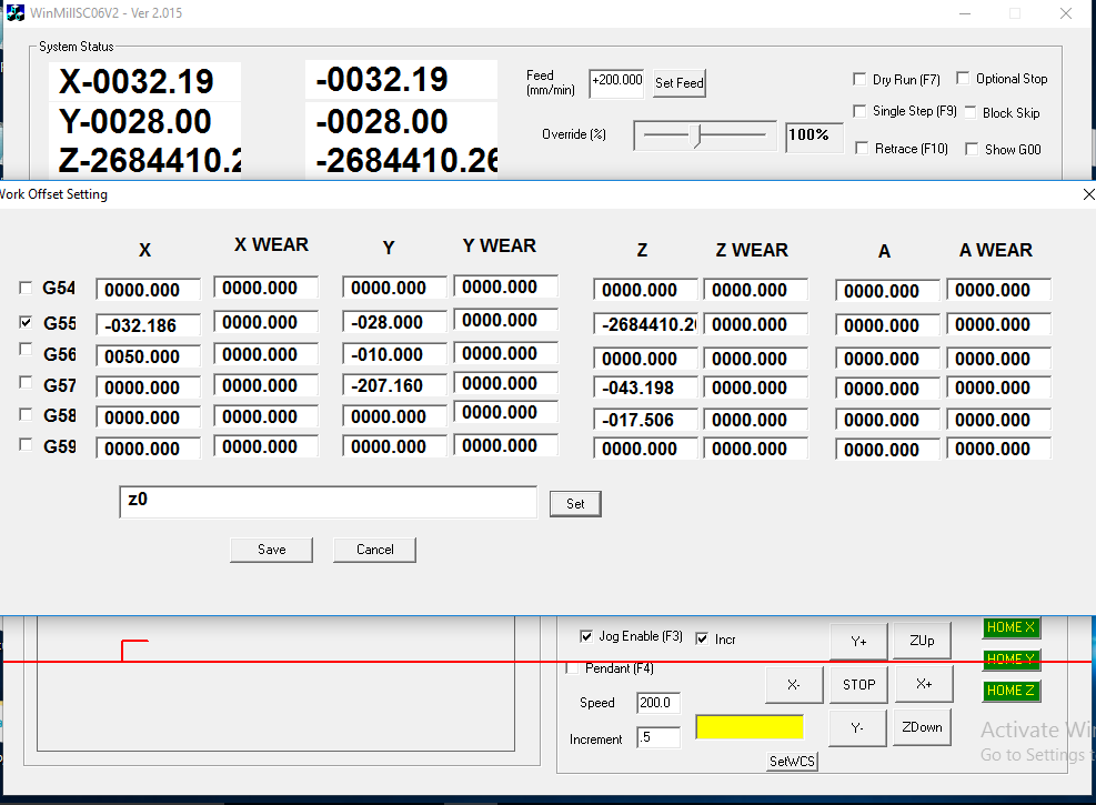
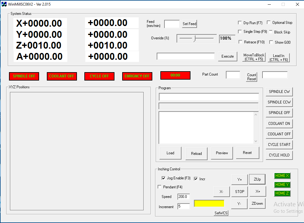
Then, click the Save button to set the origin for the PCB milling process. The screen will display the coordinates X0, Y0, Z0, confirming that the new reference point has been established.
Next, navigate to the Increments setting, configure it as needed, and click Z-Up to move the tool upward.
Then, navigate to the Load menu and select the program from the desired location.
Load the traces program to initiate the cutting process for the PCB traces.
Then, click Cycle Start to begin the milling process.
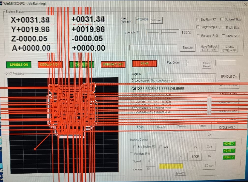
As the milling process begins, the tool rotates at a speed of 10,000 RPM, as specified in the program, and starts cutting the PCB traces.
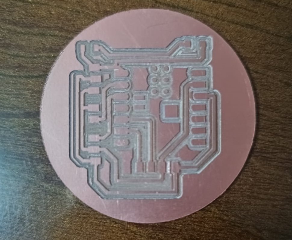
Once the traces are cut, the program is completed. Next, change the tool from a V-bit to a 0.8mm drilling tool. Then, following the same procedure, load the edge cut program while maintaining the previously set origin and click Cycle Start to begin the process.
Once the edge cut program cycle is completed, the PCB is ready for the soldering process.
PCB soldering
With the PCB milling process completed, the board is now ready for soldering. In the next step, the soldering process will be carried out.
In the soldering process, I connected the resistor, LED, connector, and ESP32-C3 board to the PCB.
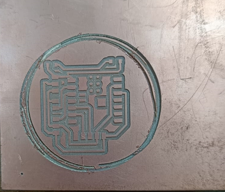
I am facing an issue where the CNC milling tool is not properly set the center of the edge, causing the entire milling process to be affected.
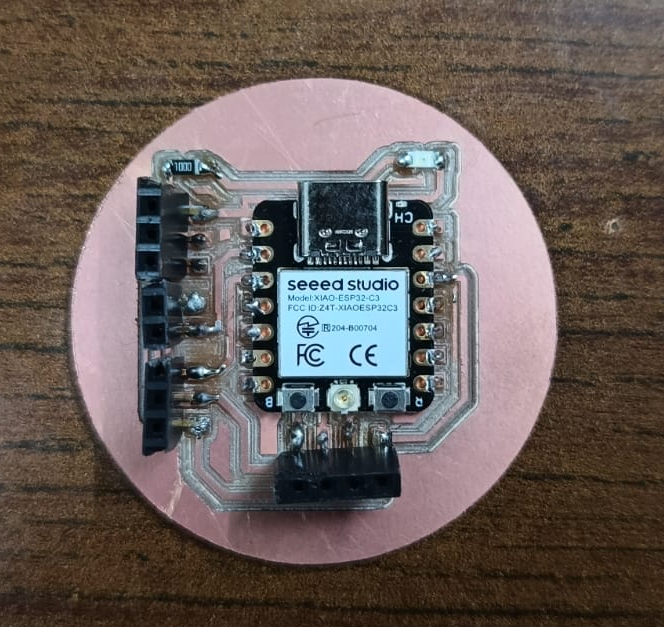
Hero Shot
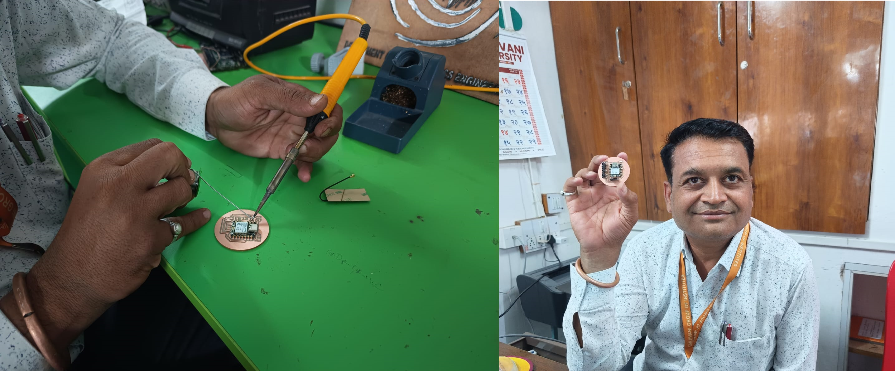
PCB Output
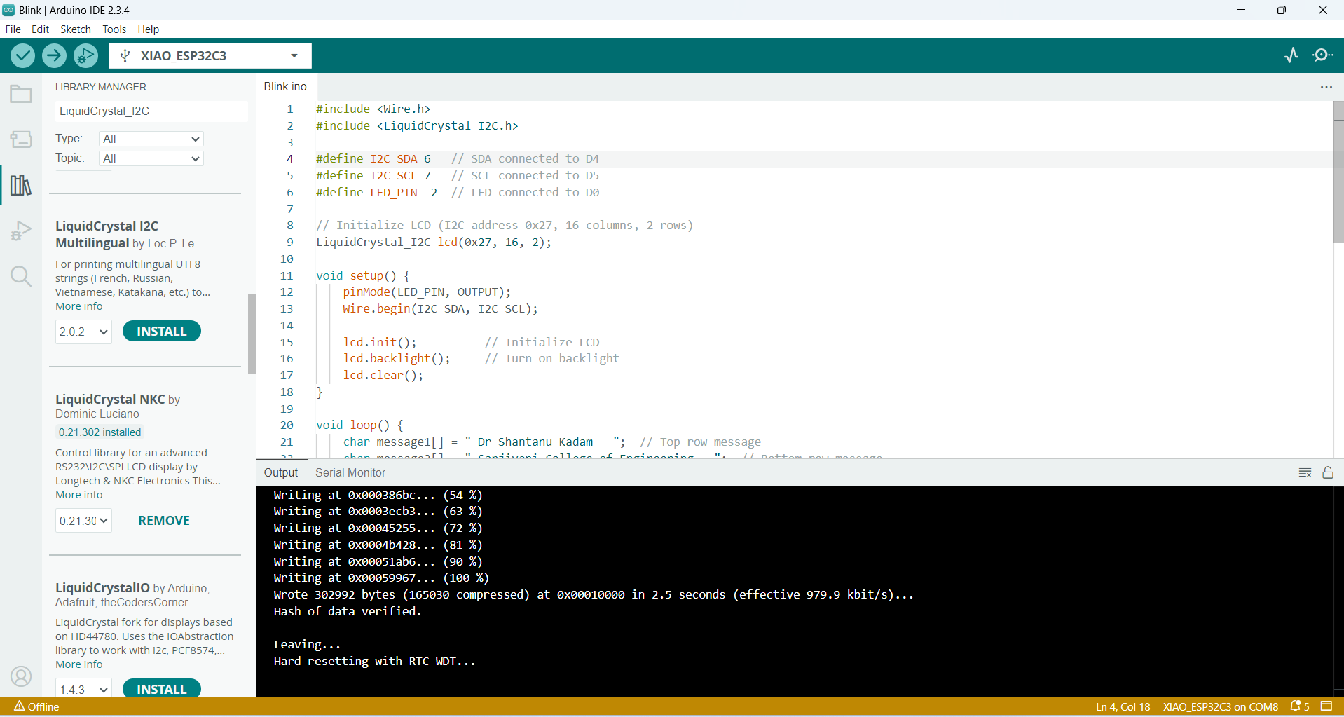
1. With the PCB finalized, the next step involves programming the I2C display. The program will display "Dr. Shantanu Kadam" on the first row and "Sanjivani College of Engineering" on the second row. This program is being developed using the Arduino IDE.
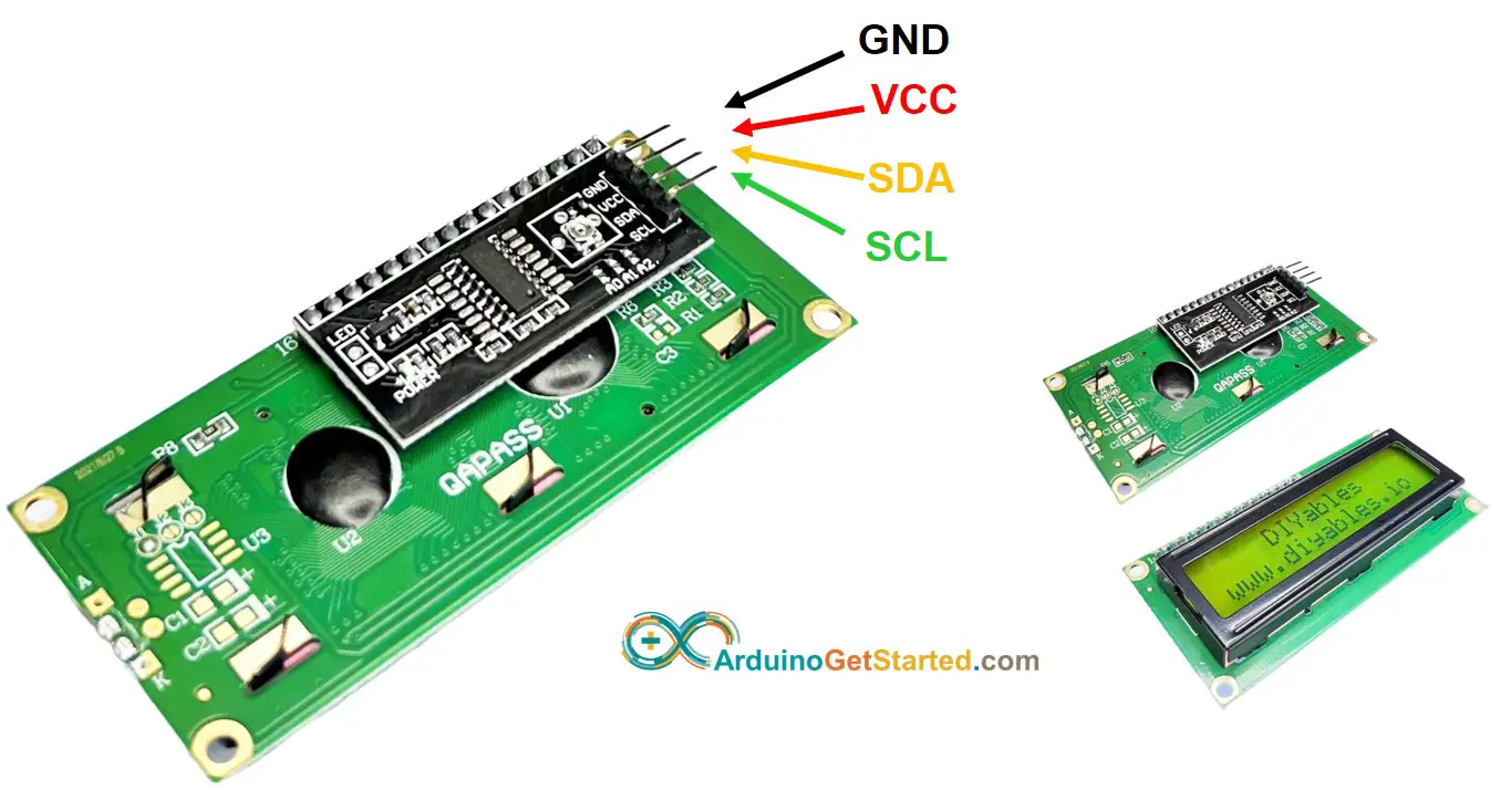
The I2C (Inter-Integrated Circuit) display is a compact and efficient interface used for displaying text and graphics. It operates using the I2C communication protocol, which is a two-wire, synchronous serial interface consisting of a data line (SDA) and a clock line (SCL). This protocol allows for seamless communication between the microcontroller and the display, enabling the transfer of data such as characters or images.
An I2C display typically features an onboard controller, such as the popular SSD1306, which interprets the data from the microcontroller and renders it visually on the screen. These displays are commonly used in projects for their simplicity, requiring fewer connections and reducing wiring complexity compared to parallel interfaces. They are well-suited for small embedded systems, such as those utilizing Arduino or other microcontroller platforms, where space and pin availability are limited.
Such displays are available in various sizes and resolutions, with OLED and LCD being the most popular variants, offering clear and energy-efficient output for a wide range of applications.
Connections
VCC* - 5V/3V3 pin (depending on breakout module)
GND* - GND
SDA - SDA
SCL - SCL
Programe Code
#include (Wire.h)
#include (LiquidCrystal_I2C.h)
#define I2C_SDA 4 // SDA connected to D4
#define I2C_SCL 5 // SCL connected to D5
#define LED_PIN 0 // LED connected to D0
// Initialize LCD (I2C address 0x27, 16 columns, 2 rows)
LiquidCrystal_I2C lcd(0x27, 16, 2);
void setup() {
pinMode(LED_PIN, OUTPUT);
Wire.begin(I2C_SDA, I2C_SCL);
lcd.init(); // Initialize LCD
lcd.backlight(); // Turn on backlight
lcd.clear();
}
void loop() {
char message1[] = " Dr Shantanu Kadam "; // Top row message
char message2[] = " Sanjivani College of Engineering "; // Bottom row message
int length1 = strlen(message1); // Length of message1
int length2 = strlen(message2); // Length of message2
for (int i = 0; i < max(length1, length2); i++) {
lcd.clear();
// Scroll "Dr Shantanu Kadam" on the top row
for (int j = 0; j < 16; j++) {
if (i + j < length1) {
lcd.setCursor(j, 0);
lcd.print(message1[i + j]);
}
}
// Scroll "Sanjivani College of Engineering" on the bottom row
for (int j = 0; j < 16; j++) {
if (i + j < length2) {
lcd.setCursor(j, 1);
lcd.print(message2[i + j]);
}
}
// Blink LED state change every 2 seconds
if (i % 8 == 0) {
digitalWrite(LED_PIN, !digitalRead(LED_PIN));
}
delay(300); // Speed of scrolling
}
}
}
Then uploading it to the XIAO ESP32-C3.
The second program focuses on controlling a motor using a relay and an LED indicator. When the motor starts, the LED stops blinking, indicating that the motor is in operation. Conversely, when the motor stops, the LED remains illuminated, signaling the motor's inactivity. This program is developed with precision to ensure seamless interaction between the relay and LED using the chosen microcontroller platform.
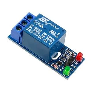
The image shows a 5V Single Channel Relay Module, commonly used in electronics and embedded systems projects to control high-voltage devices using low-voltage digital signals from microcontrollers like Arduino, Raspberry Pi, or ESP32. The relay on this module is typically of the model SRD-05VDC-SL-C, manufactured by Songle, which operates at a 5V DC input to switch AC or DC loads. It supports up to 10A at 250VAC or 10A at 30VDC, making it suitable for switching lights, fans, pumps, and other household or industrial appliances.
The module features three screw terminals (NO - Normally Open, COM - Common, and NC - Normally Closed) for connecting the load. On the control side, there are three header pins: VCC, GND, and IN. VCC connects to 5V power supply, GND to ground, and IN receives the control signal from a microcontroller. An opto-isolator (opto-coupler) is used on the board to provide electrical isolation between the control circuit and the relay, improving safety and protecting the microcontroller from voltage spikes.
Two LED indicators are also present: the red LED shows the module is powered, and the green LED indicates when the relay is active (i.e., the IN pin has been triggered and the relay coil is energized). This module is compact, reliable, and widely used in DIY automation, home control, robotics, and IoT systems where isolated switching of high-power devices is needed.
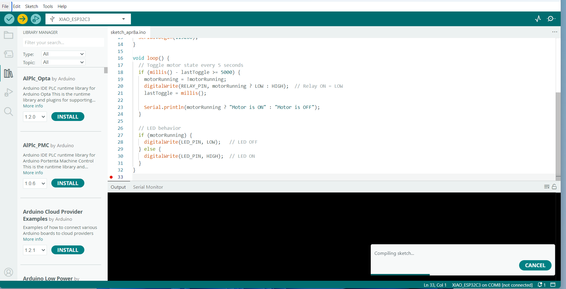
#define RELAY_PIN D0 // D0 - Relay control pin
#define LED_PIN D1 // D1 - LED pin
bool motorRunning = false;
unsigned long lastToggle = 0;
void setup() {
pinMode(RELAY_PIN, OUTPUT);
pinMode(LED_PIN, OUTPUT);
digitalWrite(RELAY_PIN, HIGH); // Relay OFF initially
digitalWrite(LED_PIN, LOW); // LED OFF initially
Serial.begin(115200);
}
void loop() {
// Toggle motor state every 5 seconds
if (millis() - lastToggle >= 5000) {
motorRunning = !motorRunning;
digitalWrite(RELAY_PIN, motorRunning ? LOW : HIGH); // Relay ON = LOW
lastToggle = millis();
Serial.println(motorRunning ? "Motor is ON" : "Motor is OFF");
}
// LED behavior
if (motorRunning) {
digitalWrite(LED_PIN, LOW); // LED OFF
} else {
digitalWrite(LED_PIN, HIGH); // LED ON
}
}
Then uploading it to the XIAO ESP32-C3.
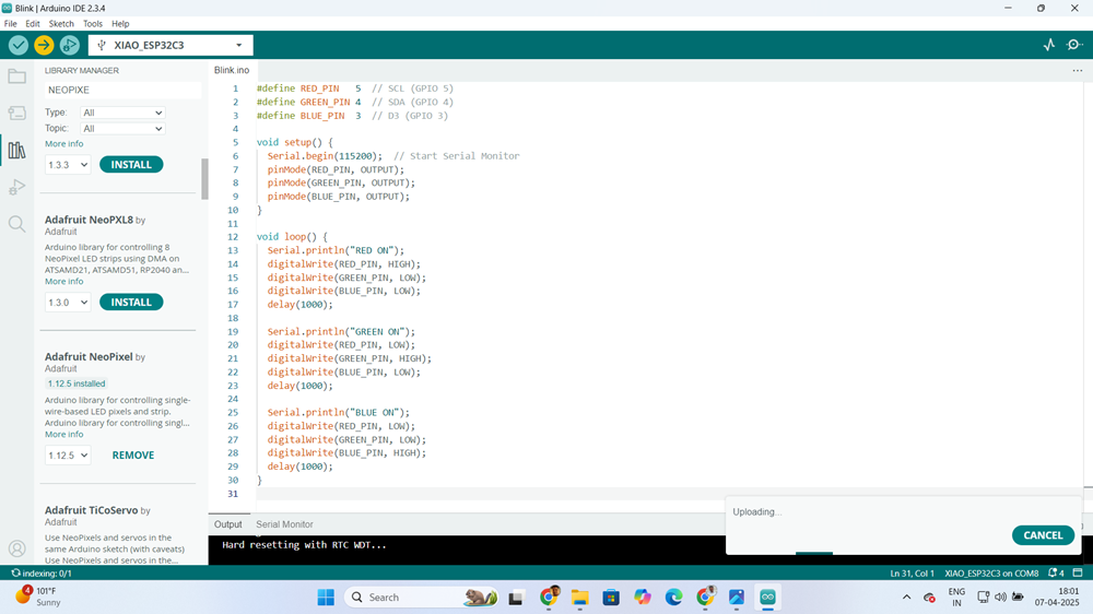
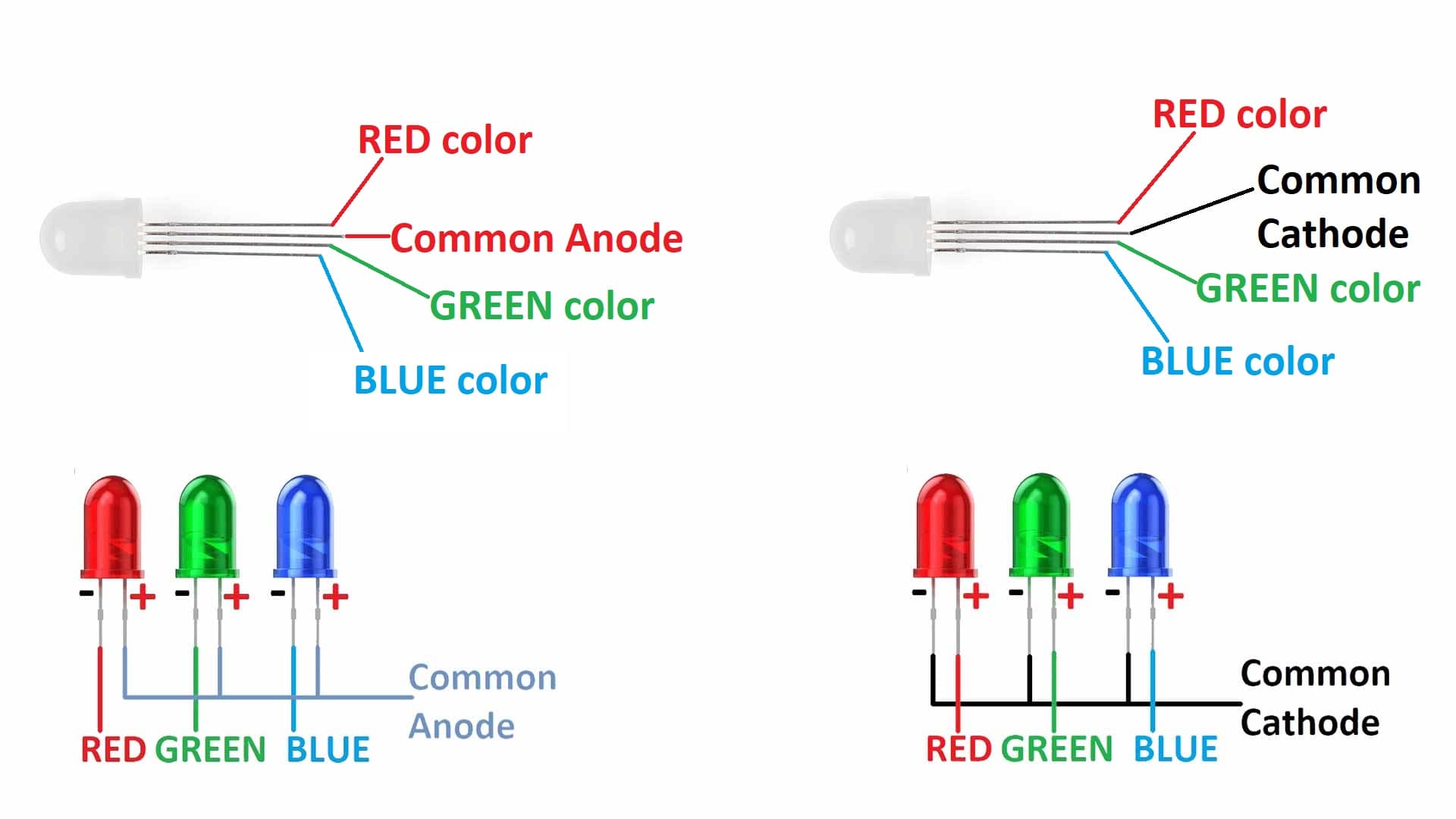
An RGB LED consists of three separate light-emitting diodes encapsulated within a single package, each capable of emitting one of the three primary colors of light: Red, Green, and Blue. These colors form the foundation of the additive color model, which is commonly used in lighting and display technologies. The red diode emits light at the longest wavelength, producing warm and vivid tones. The green diode operates at a medium wavelength and is known for its brightness and high visibility, making it effective for visual indicators. The blue diode, with the shortest wavelength, contributes cool and deep tones to the color mix. By individually controlling the intensity of each diode—typically using Pulse Width Modulation (PWM)—a wide spectrum of colors can be produced through additive mixing. For example, combining red and green yields yellow, green and blue produce cyan, and red and blue create magenta. When all three diodes are illuminated at full brightness, the result is white light. This ability to blend and create various colors makes the RGB LED a versatile component in modern electronics, including applications in digital displays, ambient lighting, and user interface systems.
#define RED_PIN 5 // SCL (GPIO 5)
#define RED_PIN 4 // SDA (GPIO 4)
>#define BLUE_PIN 3 // D3 (GPIO 3)
void setup() {
Serial.begin(115200); // Start Serial Monitor
pinMode(RED_PIN, OUTPUT);
pinMode(GREEN_PIN, OUTPUT);
pinMode(BLUE_PIN, OUTPUT);
pinMode(BLUE_PIN, OUTPUT);
>void loop() {
Serial.println("RED ON");
digitalWrite(RED_PIN, HIGH);
digitalWrite(GREEN_PIN, LOW);
digitalWrite(BLUE_PIN, LOW);
delay(1000);
Serial.println("GREEN ON");
digitalWrite(RED_PIN, LOW);
digitalWrite(GREEN_PIN, HIGH);
digitalWrite(BLUE_PIN, LOW);
delay(1000);
Serial.println("BLUE ON");
digitalWrite(RED_PIN, LOW);
digitalWrite(GREEN_PIN, LOW);
digitalWrite(BLUE_PIN, HIGH);
delay(1000);
}
}
Then uploading it to the XIAO ESP32-C3.