Week 6
Electronics design
In the study of electronics design, various measurement and analysis tools play a critical role in ensuring circuit functionality, performance optimization, and troubleshooting. The following are essential instruments and concepts in this field.
Group Assignment
I am learning about Regulated Power Supply, Multimeter, Oscilloscope, Logic Analyzer, Mixed Signal Analysis, and Multichannel Measurement as part of a group assignment with Dr. M. Sujit in the lab.
The group assignment is linked here
Indivisual Assignment
In my individual assignment, I am using an EDA tool to design a development board that incorporates components from the inventory to interact and communicate with an ESP32-C3 embedded microcontroller.
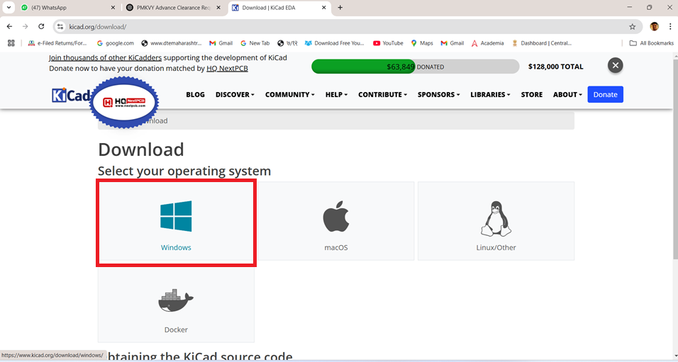
For my individual assignment, I am using the free and open-source software KiCad. I began by downloading KiCad version 9.0.0

Then, I selected KiCad 9 for Windows.
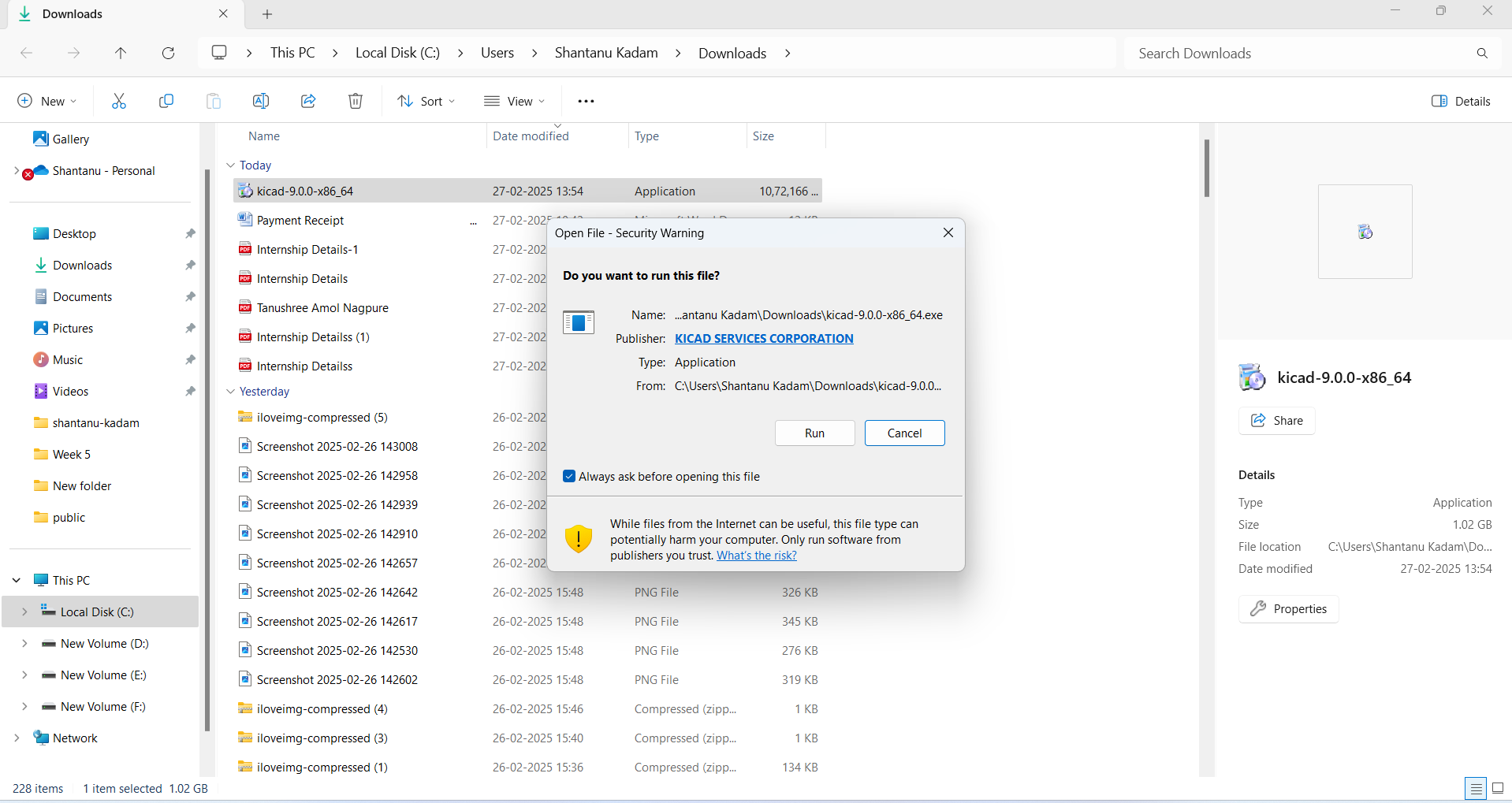
Then I select the kicad 9.0.0 folder from download and run in the laptopfot the installation of kicad software.
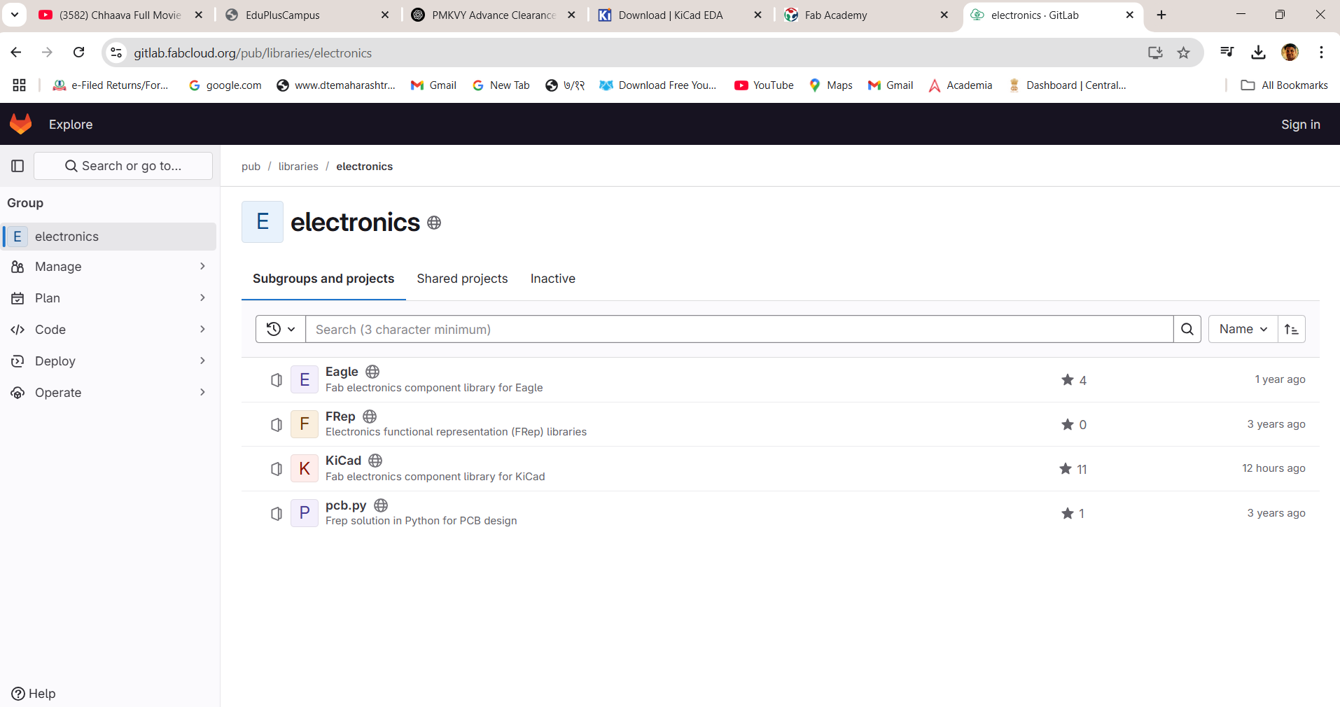
After installing the KiCad software, I accessed the Fab Library and downloaded it from FabCloud GitLab.
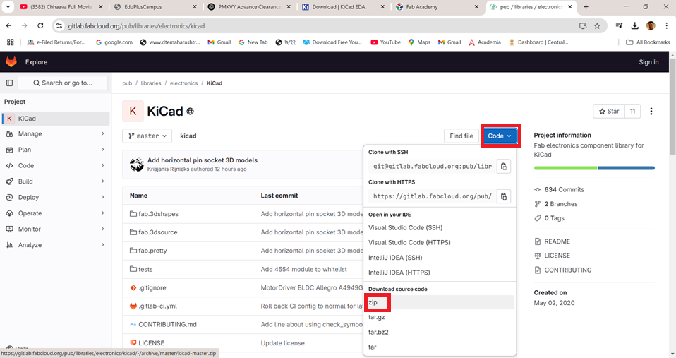
Then, I opened KiCad. Once the Fab Library was accessible in KiCad, I navigated to the code section to download the Fab Libraries ZIP file.
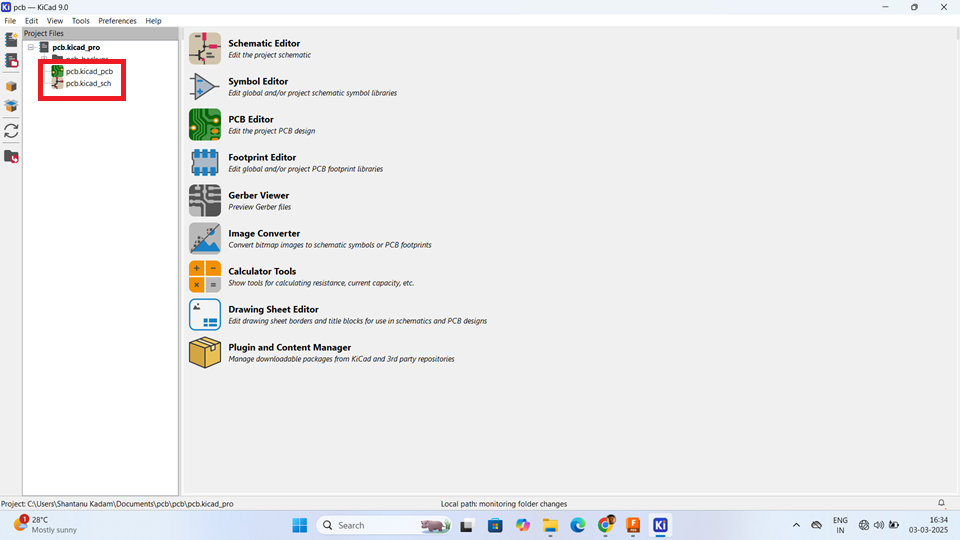
Next, I opened the previously installed KiCad software. I navigated to the File menu, selected New Project, assigned a name to the project, and saved it in the desired location. Upon creating the project, two files were generated in the project directory:
1. pcb.kicad_pcb – The PCB layout file
2. pcb.kicad.sch – The schematic file
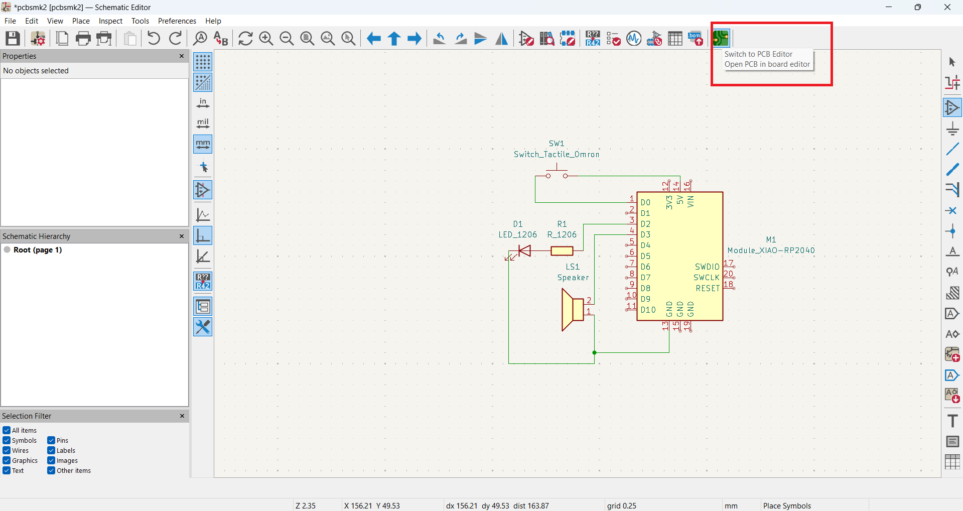
Then, I proceeded to open the Schematic Editor to begin the circuit design.
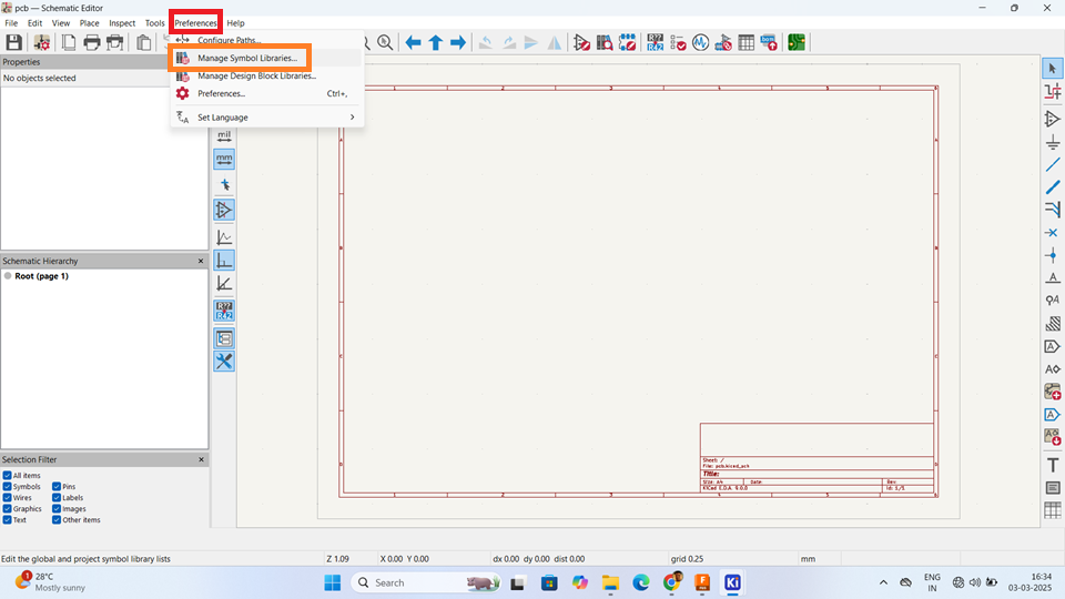
In the next step, the pcb.kicad.sch window opens. Within this window, I navigated to the Preferences menu and selected Manage Symbol Libraries.
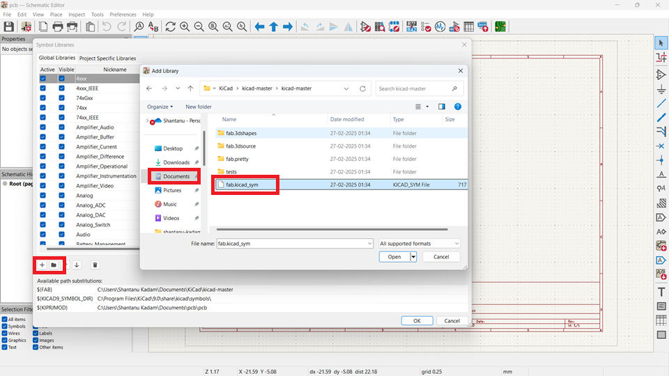
In this window, I selected Add Library Symbol and navigated to the Documents folder, where the KiCad folder was saved after download. Then, I opened the KiCad folder and selected the fab.kicad_sym file to add the symbol library.
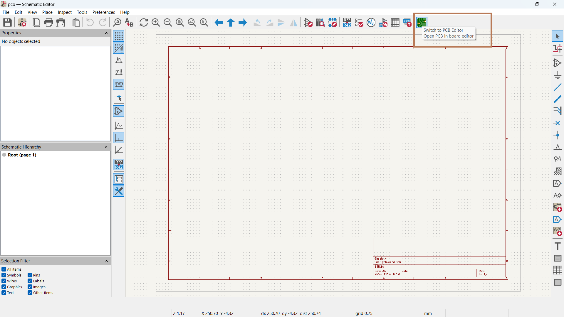
then goes into the pcb board editor for installing the foot print of the fab libraries.
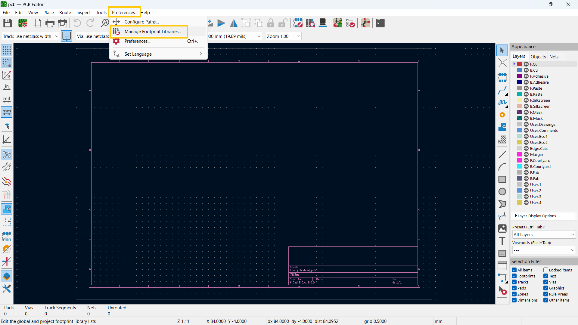
Then, I navigated to Preferences and selected Manage Footprint Libraries.
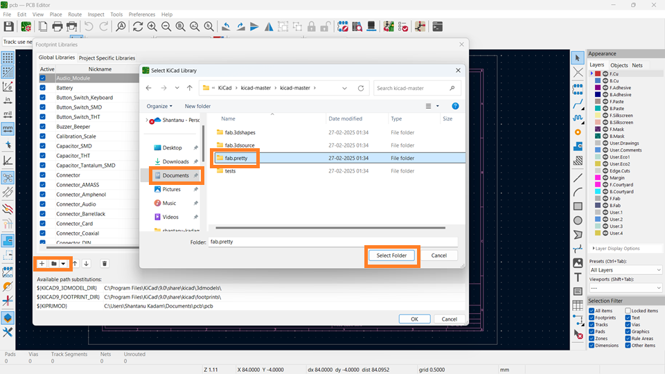
In this window, I selected Add Library Symbol, then navigated to the Documents folder where the KiCad folder was saved after download. I opened the KiCad folder and selected the fab.pretty folder to add the footprint library.
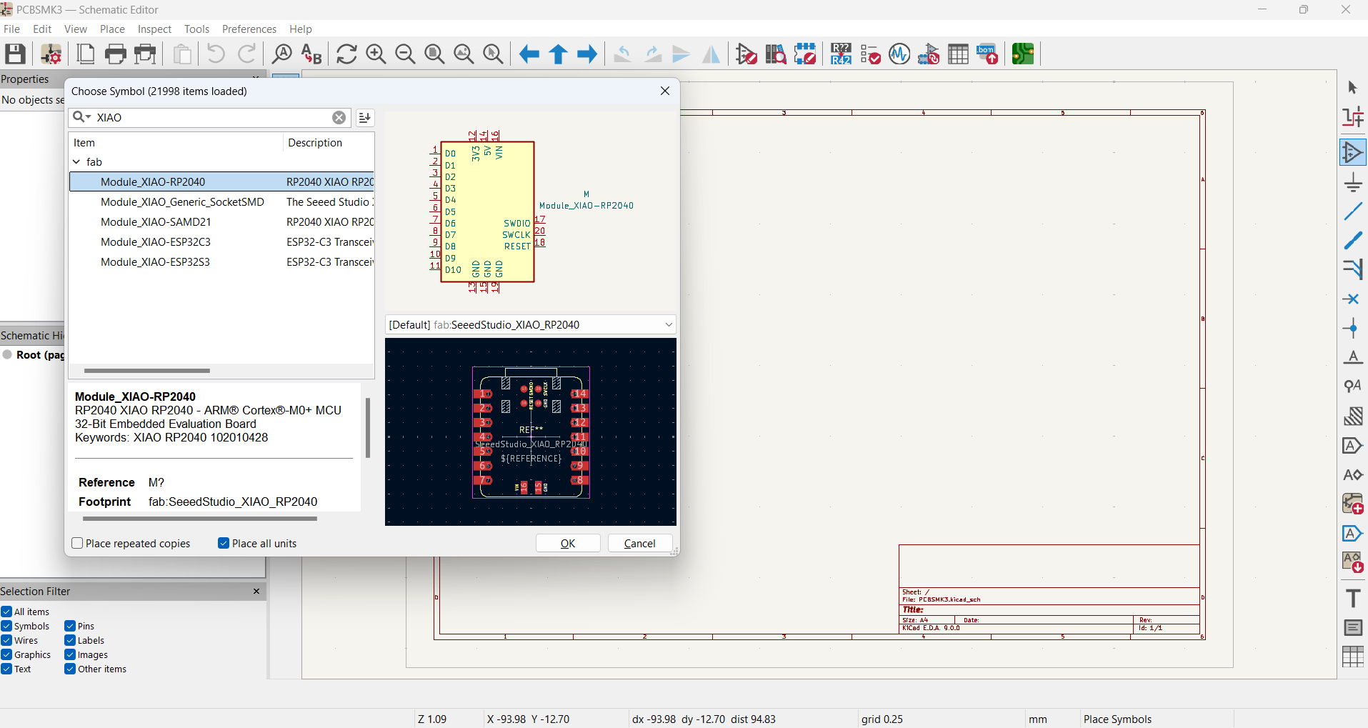
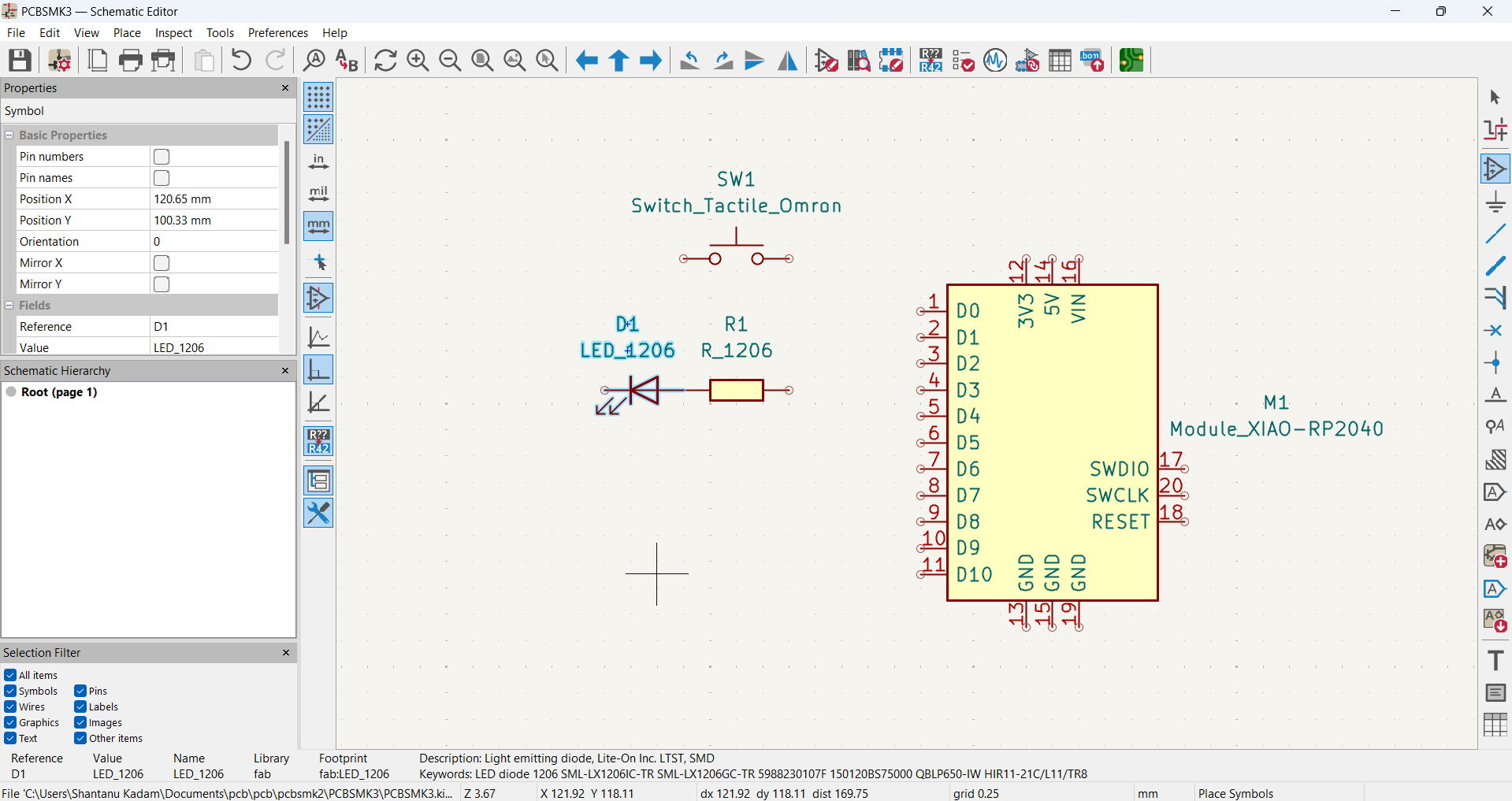
Next, I returned to the Schematic Editor and accessed the place menu to select Add Symbol. Alternatively, I used the shortcut key (Shift + A) or selected the symbol option from the right-side panel. When the Add Symbol window opened, I selected the Xiao RP2040 microcontroller along with its corresponding footprint.
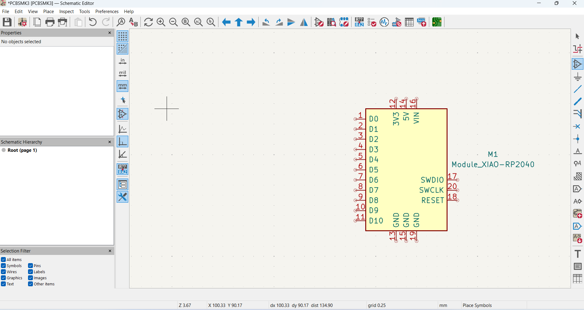
After selecting OK, the Xiao RP2040 appeared as a plus sign in the Schematic Editor. I positioned the symbol by left-clicking to place it in the desired location. To exit the Add Symbol mode, I pressed the Escape key.
Next, I added a tactile switch using the Add Symbol tool from the place menu.
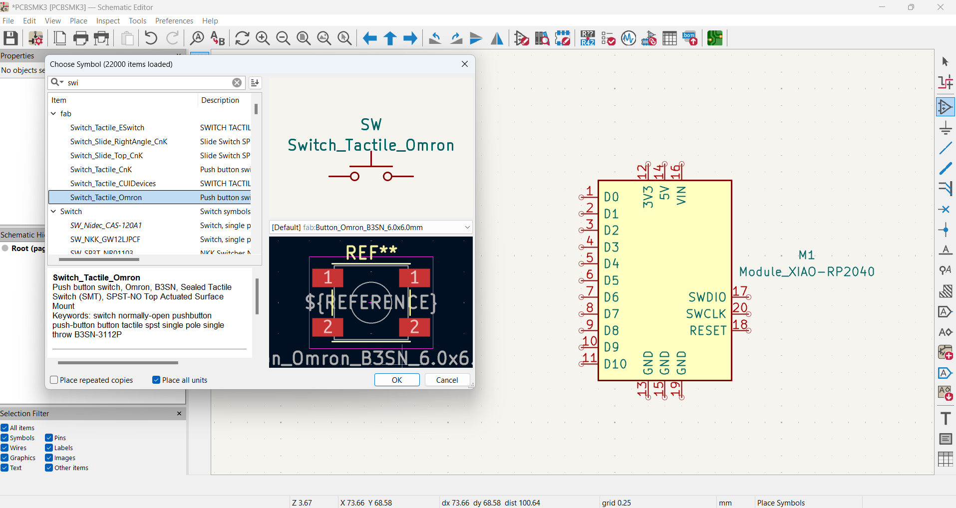
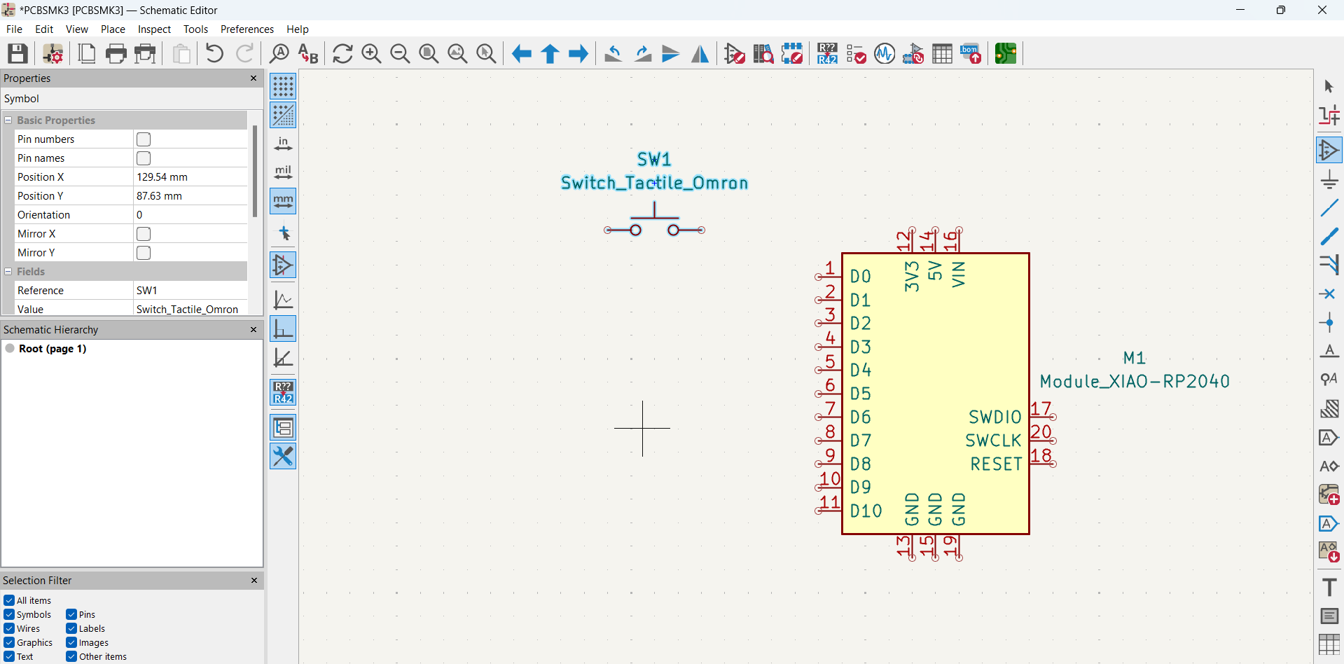
After selecting OK, the tactile switch appeared as a plus sign in the Schematic Editor. I positioned the symbol by left-clicking to place it in the desired location. To exit the Add Symbol mode, I pressed the Escape key.
Next, I added a 1206 resistor using the Add Symbol option from the Place menu. I then located the 1206 resistor in the symbol library, selected it, and clicked OK.
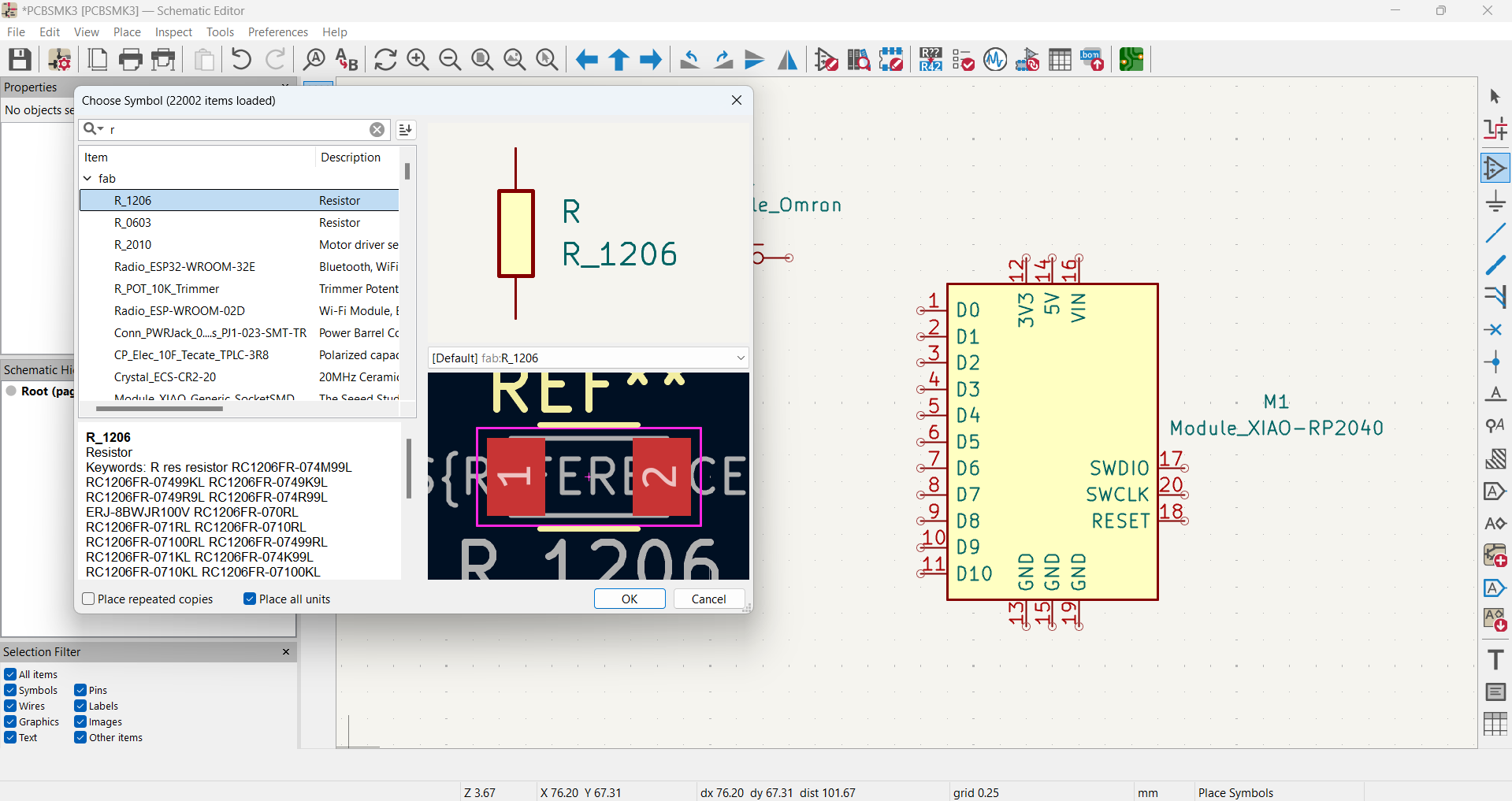
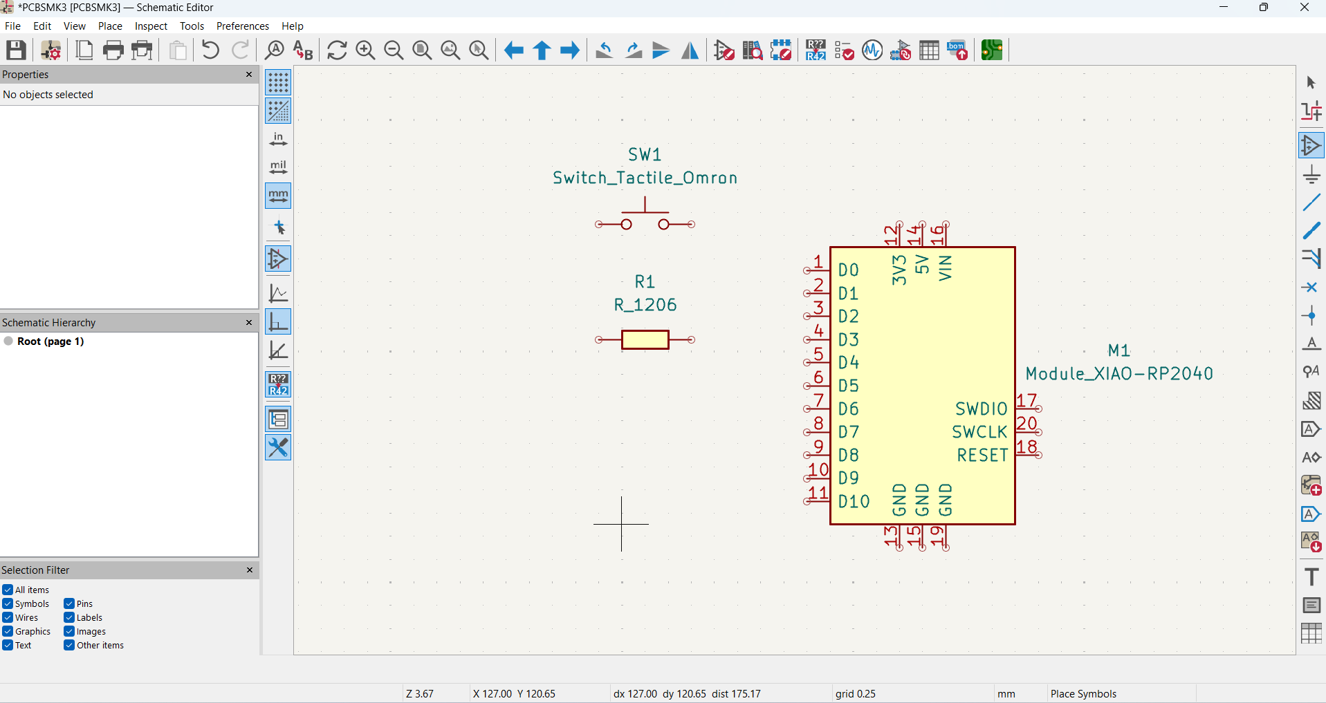
After selecting OK, the resistor 1206 appeared as a plus sign in the Schematic Editor. I positioned the symbol by left-clicking to place it in the desired location. To exit the Add Symbol mode, I pressed the Escape key.
In the same way, I added LED 1206 using the Add Symbol from the place menu.

After selecting OK, the LED 1206 appeared as a plus sign in the Schematic Editor. I positioned the symbol by left-clicking to place it in the desired location. To exit the Add Symbol mode, I pressed the Escape key.
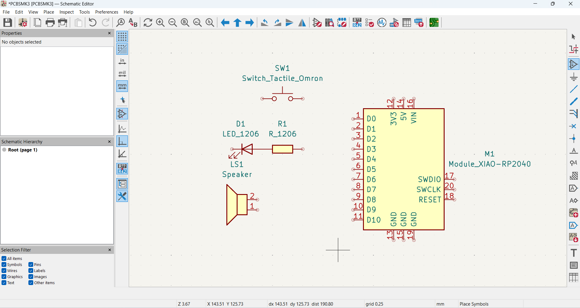
Next, I added an LS1 Speaker to my PCB using the Add Symbol from the place menu.
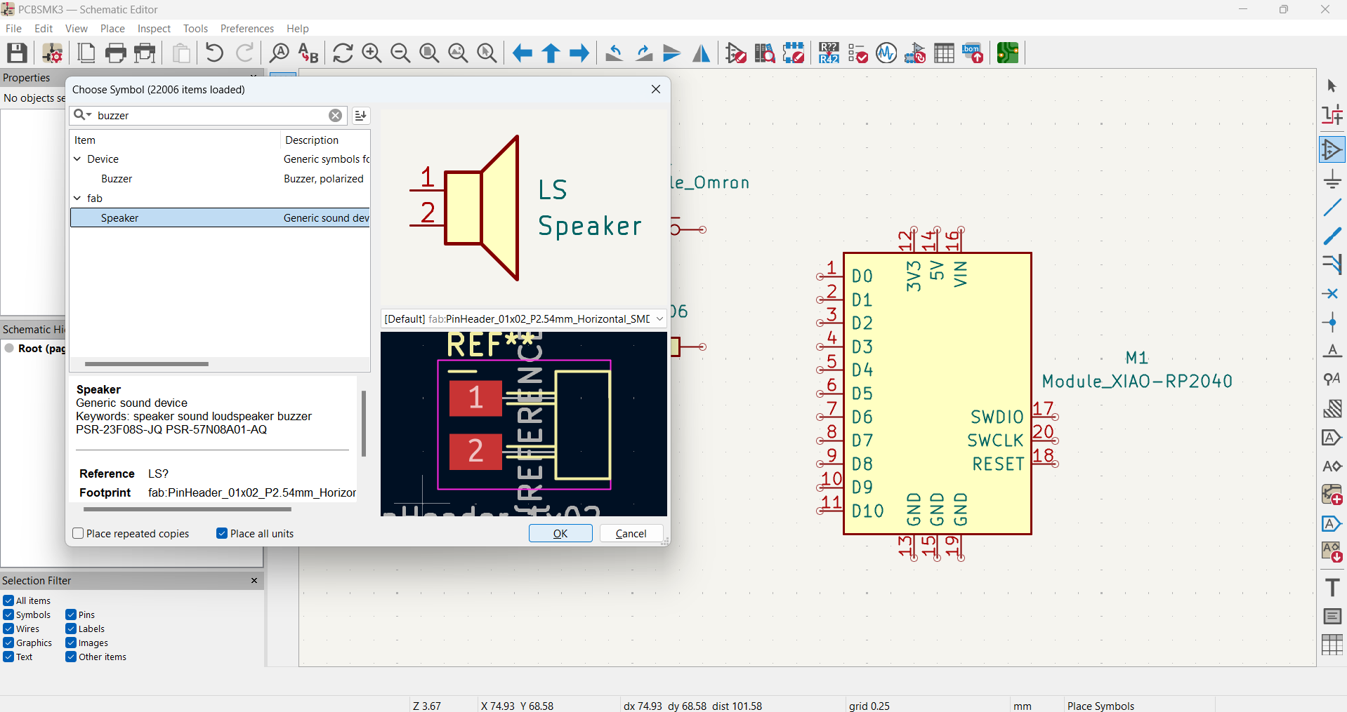
After selecting OK, the LS1 Speaker appeared as a plus sign in the Schematic Editor. I positioned the symbol by left-clicking to place it in the desired location. To exit the Add Symbol mode, I pressed the Escape key.
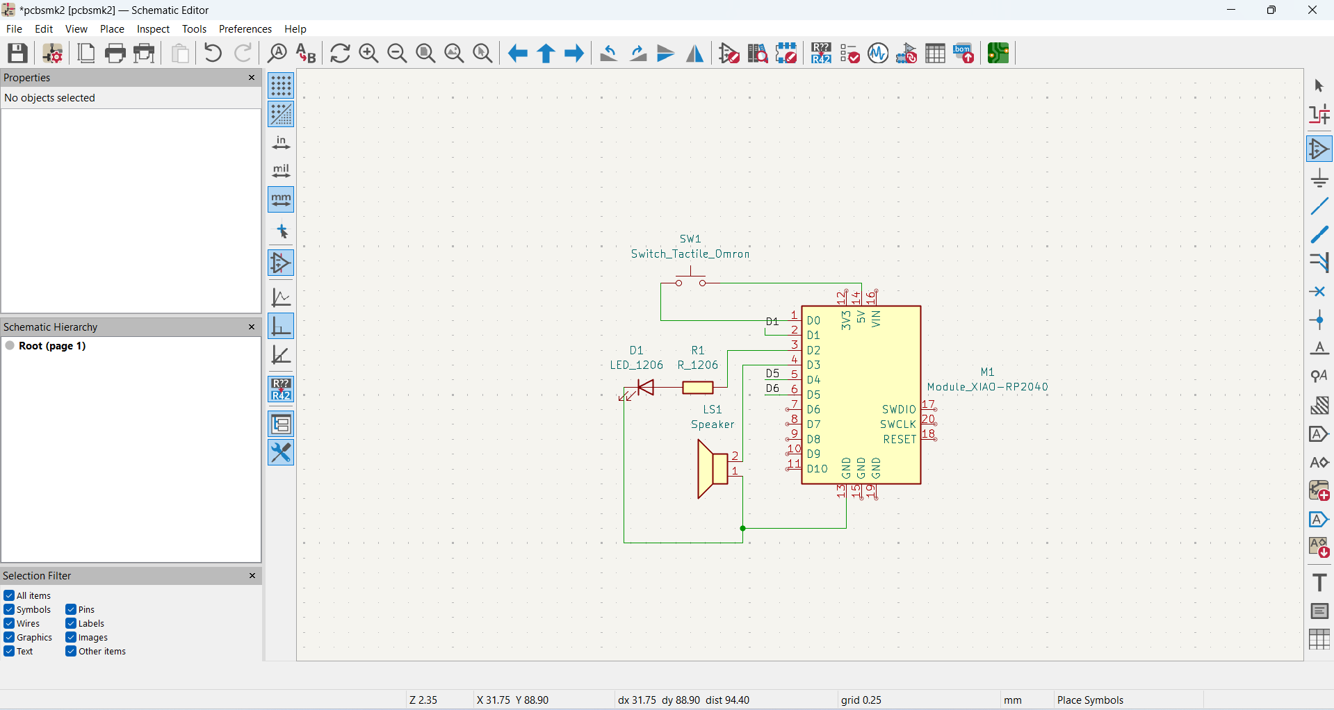
Once all the components required for my circuit diagram were added to the schematic, I began making the connections. To do this, I navigated to the Place menu and selected Draw Wire, used the shortcut key (Shift + W), or clicked the Draw Wire symbol from the right-side panel.
I then made all the necessary connections as per the circuit diagram.
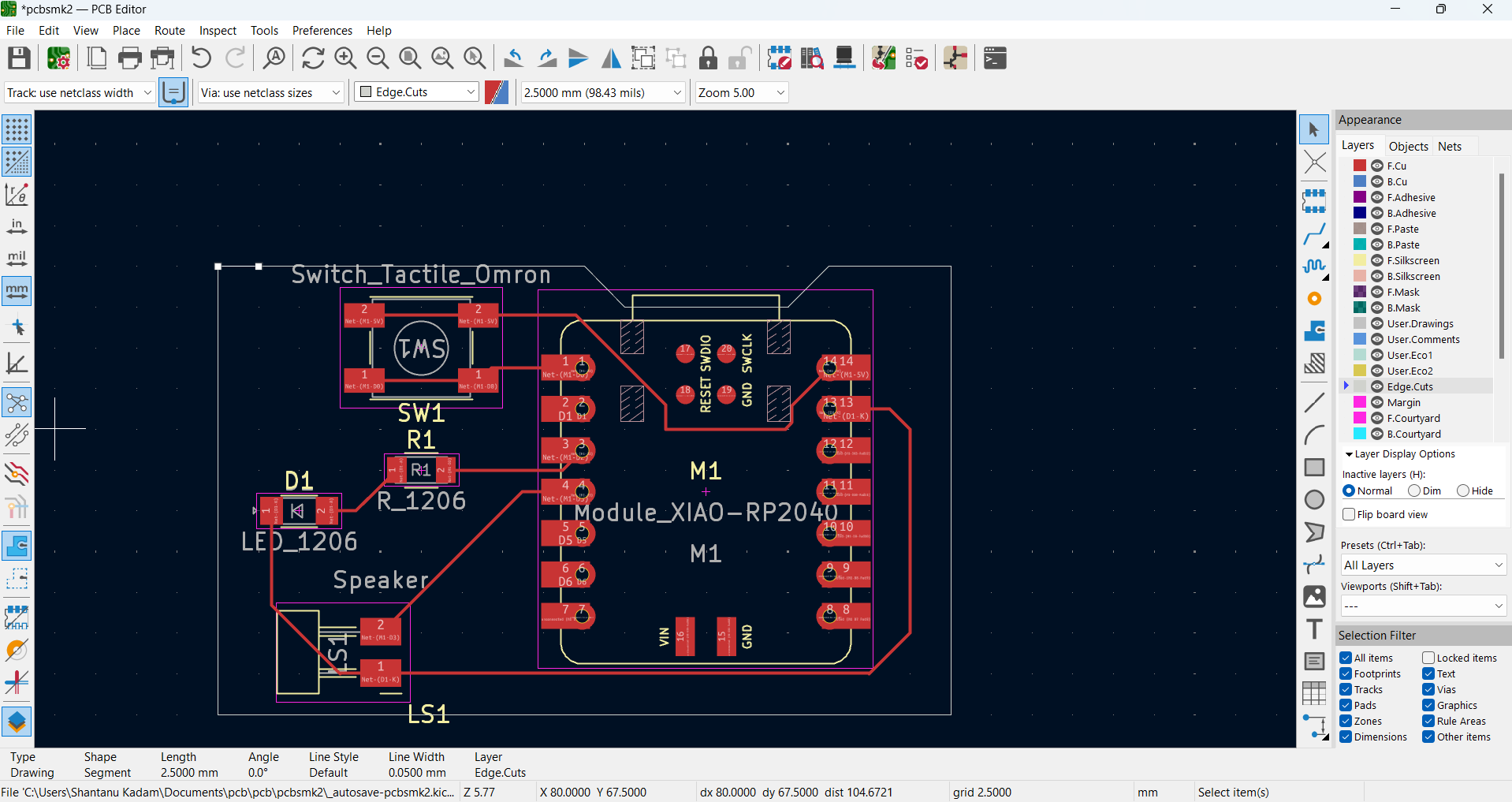
Next, I switched to the PCB Editor to open the PCB in Switch Editor.
Then, I navigated to the PCB Switch Editor.
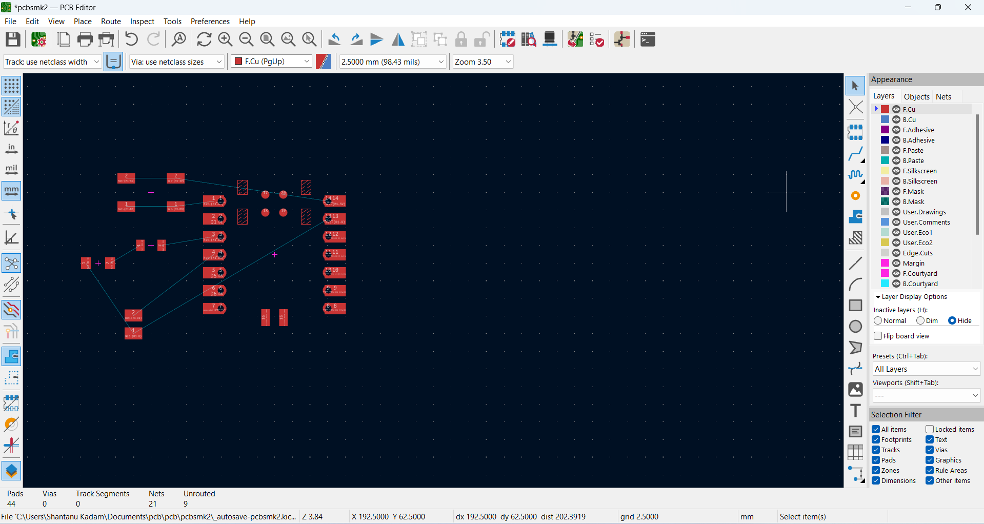
Then, I accessed the Route Track feature and proceeded with trace routing.
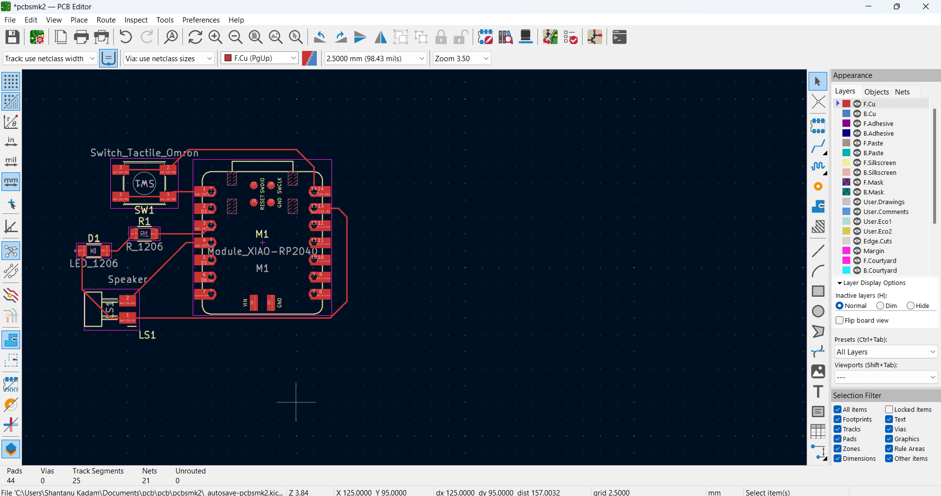
In this way, I used the Route Track feature to complete all the connections. Then, I navigated to the Inactive Layer and selected Hide.
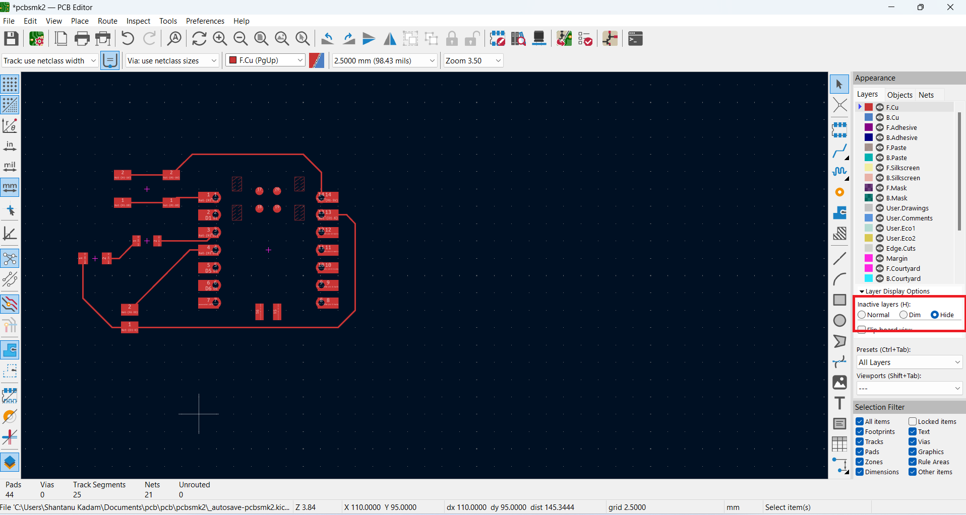
Next, it was necessary to define the PCB outline. To do this, I navigated to the Edge Cut layer, selected Draw Lines, and created the outline of the PCB.
In conclusion, learning PCB design involves a systematic approach, from adding components and making connections in the schematic to routing traces and defining the board outline. Mastering tools like the Schematic Editor, PCB Editor, and Routing Features ensures efficient circuit design and layout. With practice, attention to design rules, and proper verification, one can develop high-quality PCBs suitable for various applications.