Personal Reflection: What I Learned
This week's lab was eye-opening for me! Finally getting my hands on real test equipment instead of just reading about it made such a difference. I was honestly a bit intimidated by the oscilloscope at first - all those knobs and settings! But after our group figured out how to capture our first waveform, it started making sense.
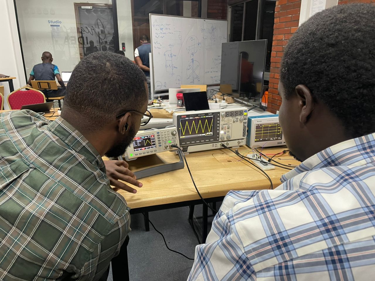
Working as a team made troubleshooting way easier. When I got stuck trying to figure out why our power supply reading was off, my teammate spotted that we hadn't properly connected the ground wire. Those "aha!" moments were the best part.
KiCad 7: My ATtiny412-SS USB Circuit Journey
I began by downloading KiCad from KiCad.org - it's free software, which is great.
After installation, I created a new project called "ATtinyusbsample" and opened the schematic editor.
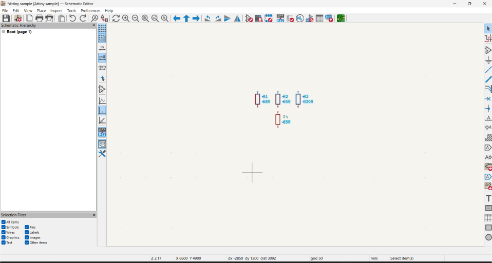
For the resistors, I searched for "R" in the component library, placed them, and then set their values and footprints. copy and past
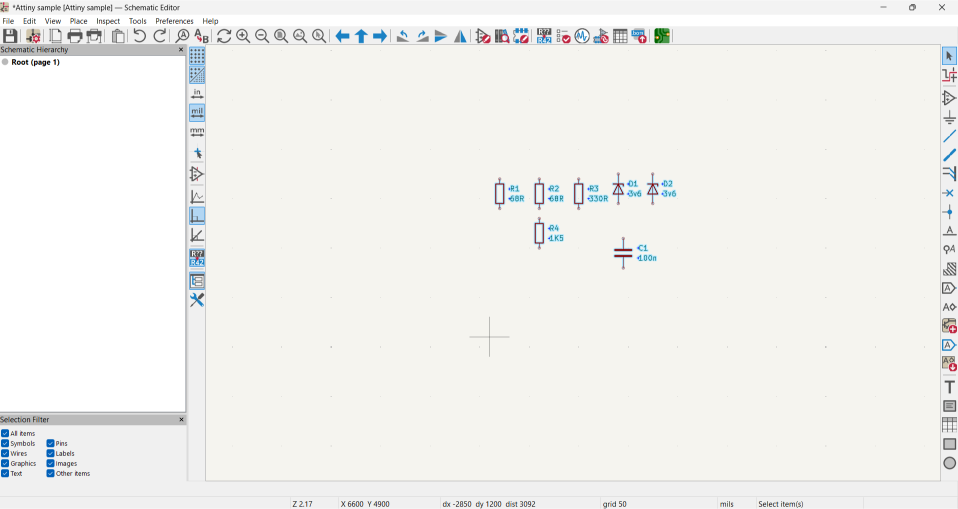
Decoupling Capacitor (C1),The 100nF capacitor was essential for stable operation:
- Searched for "C" in the component library
- Set its value to 100nF
- Selected an 0805 SMD footprint to match the resistors
- Connected it between VCC and GND directly near the microcontroller to filter power supply noise
The Zener diodes were important for USB protection
- Searched for "D_Zener" in the component library
- Placed two of them on the schematic
- Set their values to 3.6V
- Selected SOD-323 footprints for D1 and D2 (the USB protection diodes)
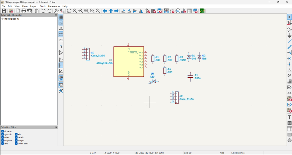
Used an 0805 LED footprint for D3 (which serves as an indicator)
- Connected D3 to one of the ATtiny's I/O pins through a resistor to serve as a status LED
Header Pins (J1, J2) (For programming and expansion:)
- Searched for "Conn_01x04" 4 pin header j1and j2
- Placed them on the schematic
- Connected J1 to the programming pins of the ATtiny Connected J2 to the remaining I/O pins and power
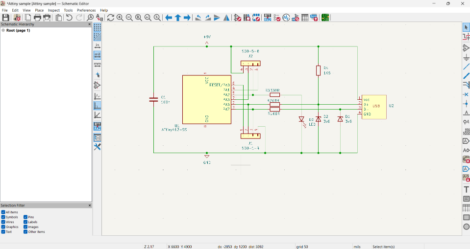
Connecting Everything Together
- After placing all components, I carefully connected them following same other USB Digispark reference design: The USB connector's D+ and D- lines connect to the ATtiny through 68Ω resistors The 3.6V Zener diodes (D1, D2) are connected to these lines for protection The 1.5kΩ pull-up resistor (R4) is connected to the D- line as required by the USB standard The 330Ω resistor (R3) is connected to one of the ATtiny's pins and the LED The decoupling capacitor is placed directly between VCC and GND All components share a common ground
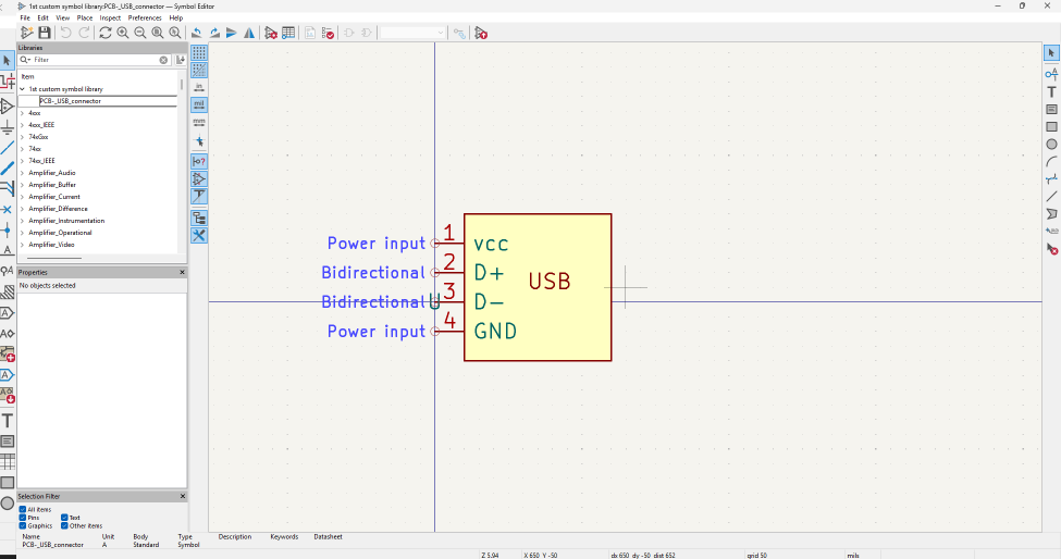
Creating Custom Parts
- For the USB connector, I needed to create both a custom symbol and footprint. In the symbol editor, I: Created a new library called "my custom symbol Library" Made a new symbol named "PCB USB Connector" Added four pins with specific properties: Pin 1: VCC (power input) Pin 2: D+ (bidirectional) Pin 3: D- (bidirectional) Pin 4: GND (power input)
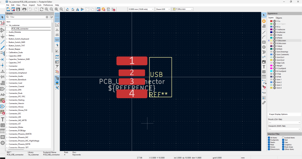
- Drew a rectangle and labeled it "USB" In the footprint editor, I created a matching footprint with: Four SMD pads with specific dimensions: Pads 1 & 4: 7mm × 2mm Pads 2 & 3: 6mm × 1.5mm Positioned at -3.75mm, -1mm, 1mm, and 3.75mm Added silkscreen text reading "USB" Created a 5mm keep-out zone to prevent other components from being placed too close
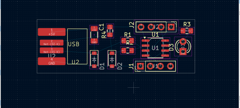
After completing the schematic, I generated the PCB layout using the "Update PCB from Schematic" tool. First, I defined a board outline of 14mm × 12.2mm using the edge cuts layer. Then I arranged all the components within this outline, keeping in mind: The USB connector needed to be positioned at the edge The ATtiny needed enough space for all its connections Components should be spaced to make soldering easier
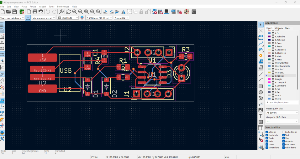
I connected everything with tracks, using vias where I needed to change layers, but it took me a long time to do it.
I searched on how to do the autoroute then go through the description
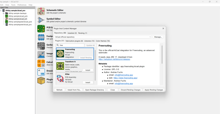
went to plugin and searched for freerouting
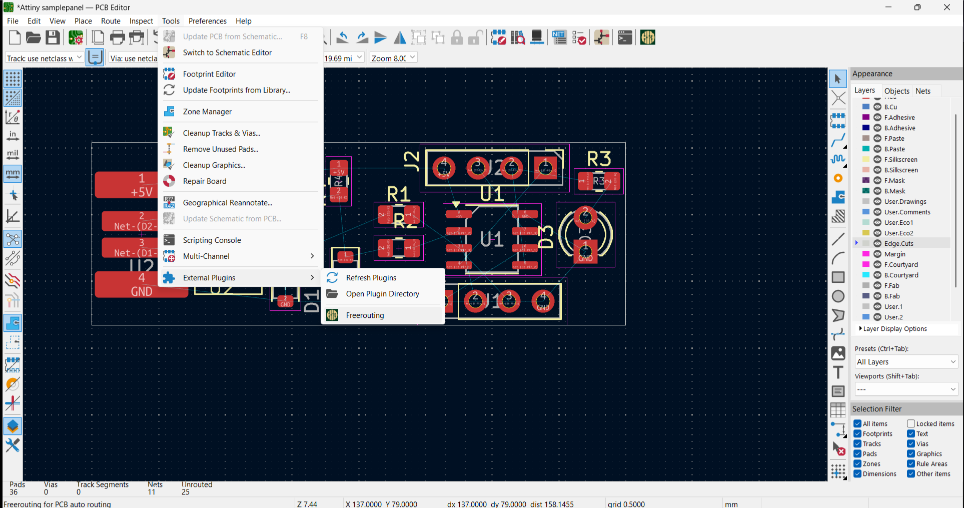
Back to PCB editor and tool,then External plugins clicked

the result was fast and good campare to mine
Manual Routing vs. Auto Routing: My Experience
During this project, I experienced both manual and automatic routing approaches, which helped me understand their differences:
Manual Routing:
- Initially, I tried to manually route all the connections on my ATtiny board
- This gave me complete control over the exact path of each trace
- I could prioritize critical paths like the USB data lines (D+ and D-)
- I found it was better for signal integrity as I could keep sensitive traces short and direct
- The process was very time-consuming and required significant patience
- It was excellent for learning the fundamentals of PCB layout, but quite challenging
Auto Routing:
- After struggling with manual routing, I discovered the FreeRouting plugin
- The auto-router completed in seconds what took me hours to do manually
- It produced a workable solution but sometimes made strange routing decisions
- The tool was incredibly efficient but lacked the "design intent" that manual routing provides
- For complex boards, I found a hybrid approach works best - manually route critical signals, then let the auto-router handle the rest
For beginners, I'd recommend starting with manual routing to understand the principles, then using auto-routing tools to save time on non-critical connections. This gives you both the understanding and the efficiency!
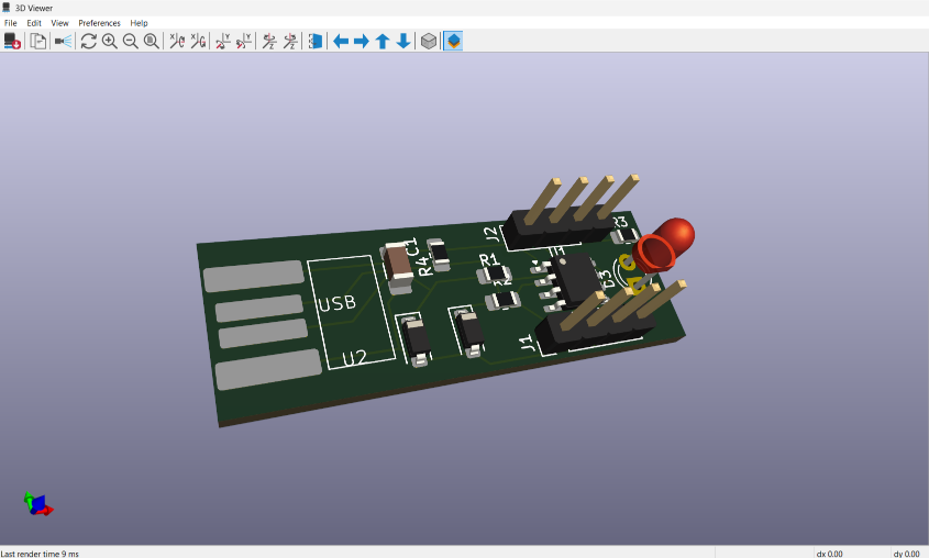
my 3d view front
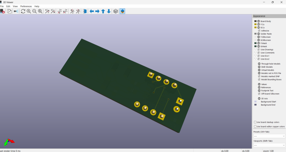
my 3d view back
KiCad: My XIAO RP2040 Interface Board Journey
I started by set up the Fablab library using these steps:
- Downloaded the library from Fablab kicad library
- Located the zip folder in my downloads and extracted it to my documents folder
- Opened KiCad and went to "Preferences / Manage Symbol Libraries"
- Added fab.kicad_sym as a symbol library
- Went to "Preferences / Manage Footprint Libraries"
- Added fab.pretty as a footprint library
- Went to "Preferences / Configure Paths" and added new environment variable "FAB" pointing to the library location
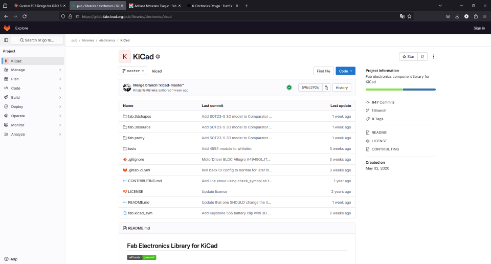
Adding the XIAO RP2040 Module (M1)
- For the main microcontroller module, I added the XIAO form fab libraries
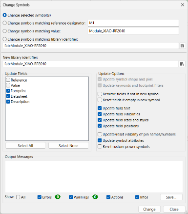
Creating the custom symbol for the XIAO RP2040 module with all the necessary pins.
Adding Pin for Interfaces
- Searched for "fab:PinHeader_01x06" for the 4 and 6-pin headers
- Placed several connectors on the left and bottom sides of the schematic
- Named them according to their functions (I2C, UART, SPI, GPIO)
- Added power and ground connections to each connector as needed
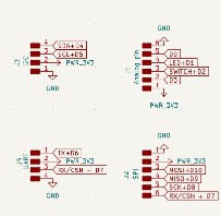
Placing the connector symbols and assigning appropriate pins for each interface.
Push Button (SW1) and LED Circuit (D1)
- Searched for "SW_Push" in the component library for the tactile switch
- Connected it between the SWITCH+D2 pin and GND
- Added an LED with two resistors (R1 and R2) to limit current
- Connected the LED circuit to the LED+D1 pin of the XIAO module
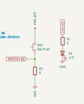
Adding the user interface components - push button and LED with current-limiting resistors.
Connecting Everything Together
- Connected all power pins to the PWR_3V3 power net
- Connected all ground pins to the GND net
- Connected the I2C pins (SDA+D4, SCL+D5) to their respective connectors
- Connected the UART pins (TX+D6, RX/CSN+D7) to their connectors
- Connected the SPI pins (MISO+D9, MOSI+D10, SCK+D8) to their connectors
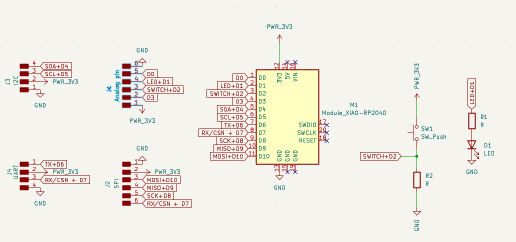
The completed schematic with all components properly connected according to the design requirements.
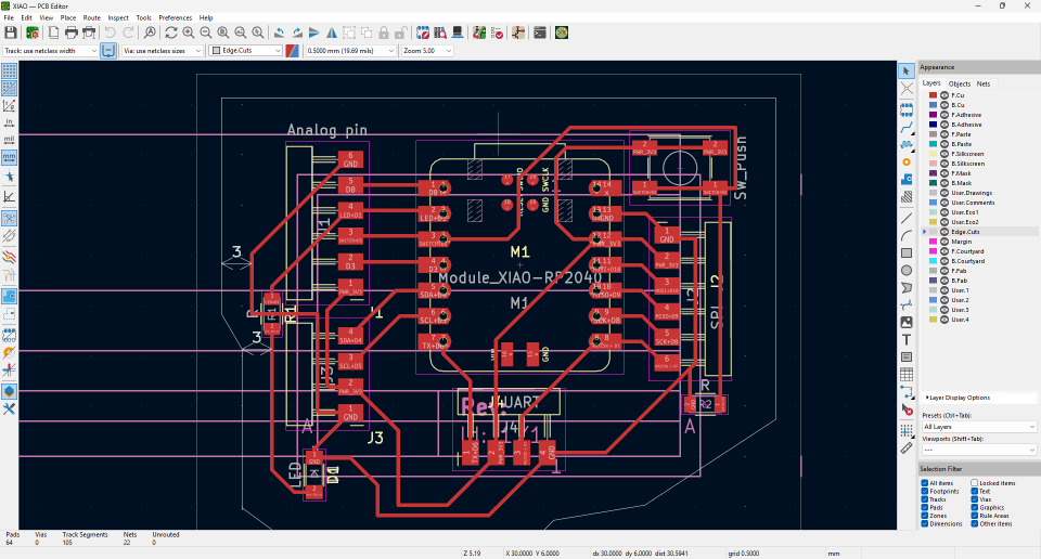
bcp editor with all connection connected
PCB Layout
- After completing the schematic, I generated the PCB layout using the "Update PCB from Schematic" tool
- Defined a board outline of 50mm × 40mm using the edge cuts layer
- Positioned the XIAO RP2040 module in the center of the board
- Arranged the connectors along the edges for easy access
- Placed the LED and push button on the right side for user interaction
Final Result
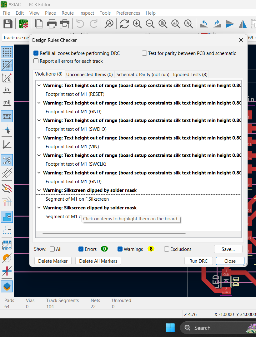 Ran the Design Rules Check (DRC) to ensure no errors, just warning
- Verified all connections matched the schematic
- Generated 3D views to visualize the final board
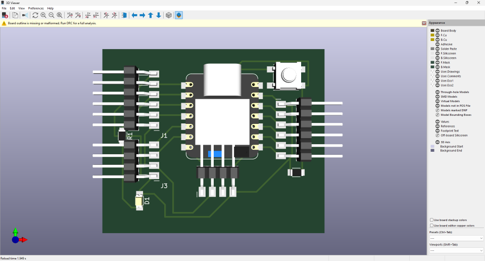
My 3D view showed me the error i made when place the blue print of the connector
Challenging Rotated Pin Header: My Solution
One of the most frustrating issues I encountered during my XIAO board design was improperly rotated pin headers. When I my instructor viewed my 3D model, he saw that one my pin headers were rotated from their intended orientation!
- In the screenshot above, you can see the pin headers are incorrectly positioned - they're rotated sideways instead of facing outward
- This happened because I placed the footprints without checking their orientation in the 3D viewer
- With this orientation, the pins would be unusable in the final board - they would face the wrong direction and make connections impossible
- Simply moving the components wouldn't fix the issue because the traces would still connect to the wrong pins
- First, I selected each problematic pin header footprint in the PCB editor
- Right-clicked and chose "Properties" to open the footprint properties dialog
- In the "Orientation" section, I adjusted the rotation by -90 degrees to correct them
- After rotating, I had to slightly adjust the position of each connector to maintain proper spacing
- Finally, I ran the DRC check again to make sure no connections were broken
This experience taught me an important lesson about PCB design: always check your component orientations in 3D view before completing your routing! It's much easier to fix orientation issues before you've connected all the traces.
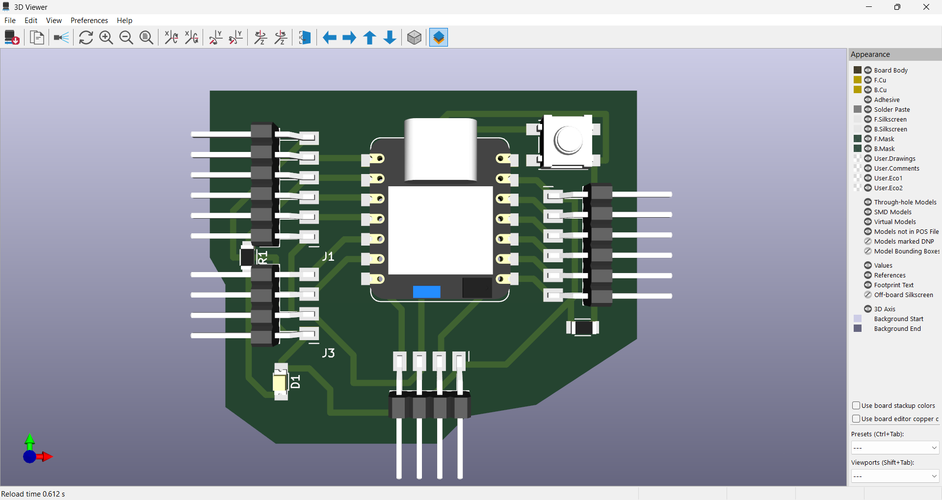
My 3D view corrected - notice how the pin headers now face outward for easy connection
- ORGINAL File for PCB Desing Attiny sample
- ORGINAL File for for PCB Desing XIAO