Assignments
Group Assignment:
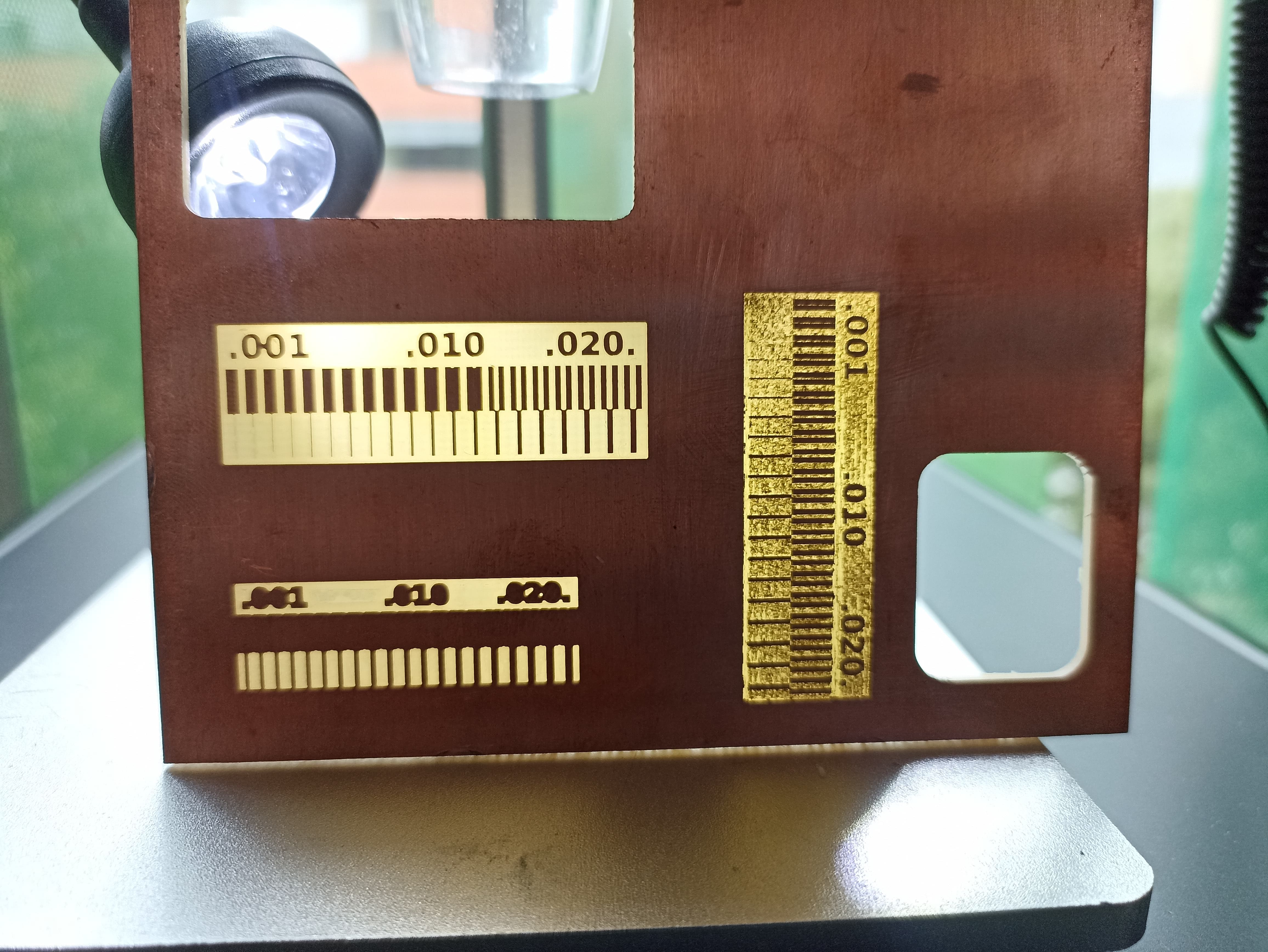
- Characterize the design rules for your in-house PCB production process: document
feeds, speeds, plunge rate, depth of cut (traces and outline) and tooling.
- Document the workflow for sending a PCB to a boardhouse.
- Document your work to the group work page and reflect on your individual page what
you learned.
Individual Assignment:
- Make and test a microcontroller development board that you designed.
Week 8. Electronics Production
Reflections on Group Work and Personal Learning
This week, I wasn’t able to coordinate with my official group members in the Fab Lab due to scheduling conflicts. However, I collaborated with another student from the university who was also exploring PCB fabrication for her personal projects.
Together, we explored two approaches: using a CNC router and a fiber laser. While the CNC router allowed us to engrave traces and drill holes with precision, we were particularly curious about testing the capabilities of the fiber laser. My specific contribution was focused on this area — I performed multiple engraving tests with the fiber laser to evaluate its ability to cleanly remove copper.
After the first trials, I refined the parameters and made a second engraving attempt with improved speed, focus, and power settings. This improved the clarity of the traces and gave us a more realistic view of what’s achievable with this tool in our context. These findings were documented and compared directly against the CNC results.
Although the fiber laser offered fast and precise engraving, we confirmed that it lacks sufficient power to perform through-hole cuts, which are essential for most PCB designs. This limitation ultimately led us to rely more heavily on the CNC approach.
Another aspect I contributed to was validating the external fabrication workflow using JLCPCB. I carried out the complete procedure — from exporting the Gerber and drill files in KiCad, to uploading and configuring the order on the JLCPCB platform. I documented each step including how to check the layer previews, select board specifications, and set production quantities. This guide served both my own fabrication and future references for others.
Additionally, during our group testing phase, we identified inconsistencies in hole alignment when using some CAM software configurations. This insight helped me adjust my own workflow to avoid misalignment issues during soldering and component mounting. We also shared notes on feeds, spindle speeds, and optimal cutting depths for triplex boards.
This joint experience gave me a stronger technical understanding of the available fabrication methods, and prepared me well for my individual board production later in the week.
2). Introduction
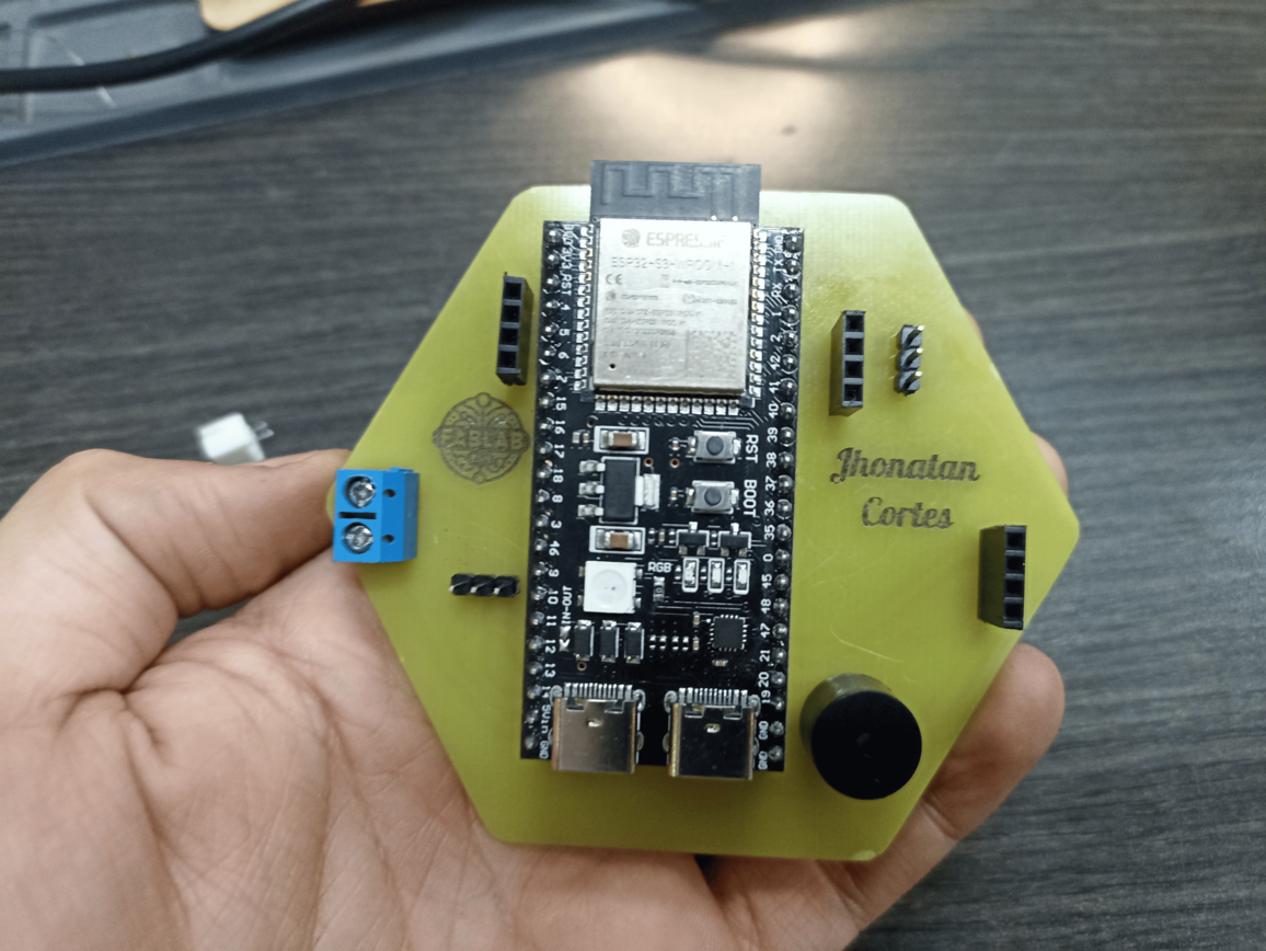
For this week’s assignment, I decided to fabricate the same expansion shield I designed during Week 6 – Electronics Design. The board was originally created to serve as a modular platform for connecting and testing different sensors and actuators with the ESP32-S3.
My goal was to take that digital design and bring it into the physical world, using CNC manufacturing techniques. I will explain the full production workflow: from CAM preparation, toolpath generation, machine setup, and engraving, to soldering and testing the final board.
Since I had already validated cutting parameters and tool types during the group work, I was able to apply that knowledge directly to my personal PCB. This allowed me to work confidently and avoid common mistakes. My process combines digital design, machine operation, and hands-on electronics assembly — and marks a key milestone in moving from virtual prototype to functional hardware.
3). Board Design (See Week 6)
The board I chose to fabricate this week is the same expansion shield I designed in Week 6 – Electronics Design. From the beginning, I planned that board with manufacturability in mind, so all dimensions and component placements were created with single-layer CNC fabrication as the goal.
Below you can see the final PCB layout ready for production, as well as a clean DXF version of the board outline that was exported for CNC milling.
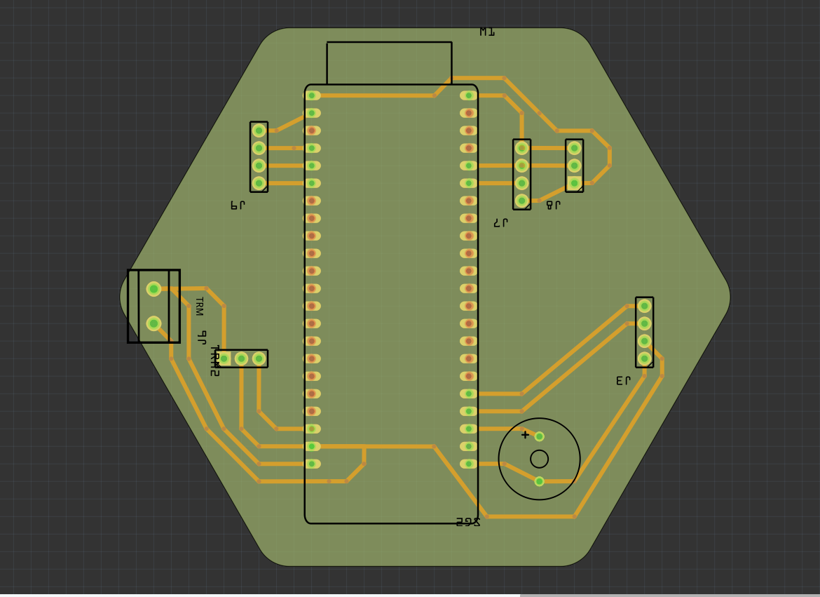
This is the board I will manufacture. It includes multiple headers, a buzzer, and a power terminal, designed to help me test various sensors.
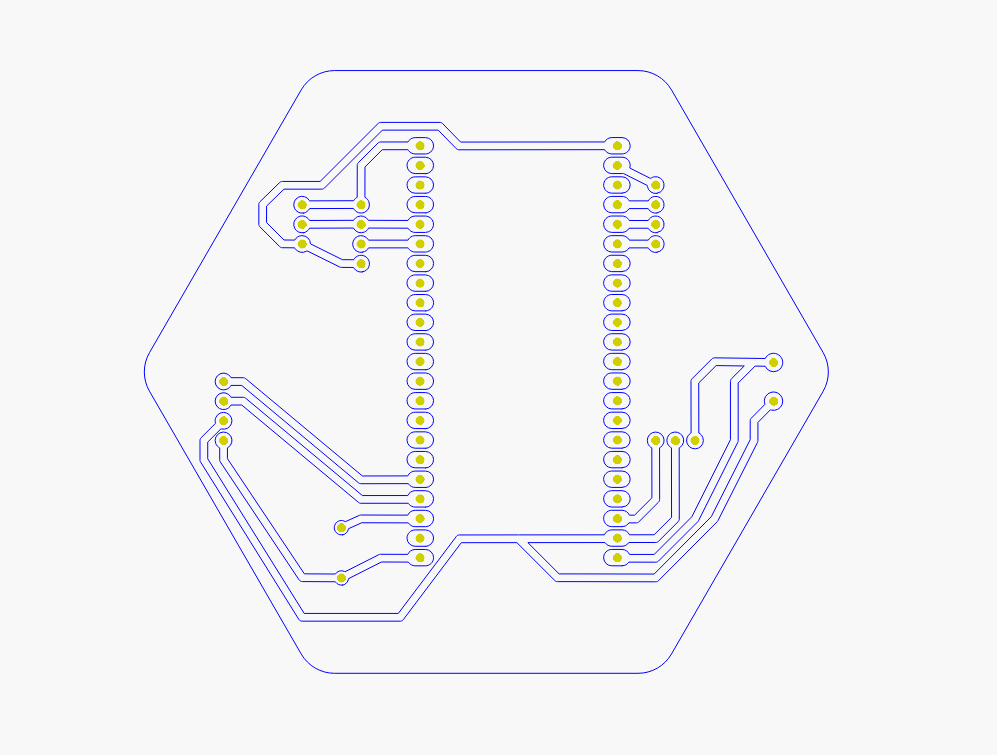
Clean DXF file exported from Fritzing and prepared for CAM processing in Fusion 360. This is the format used by the CNC machine.
If you want to learn more about how I created this board — from software selection to component placement — feel free to visit my Week 6 documentation at the following link:
4). Fabrication Workflow (Fusion 360 + Makera Carvera)
Now that the design is ready, I focused entirely on the manufacturing process. The machine I used for PCB milling is the Makera Carvera, a desktop CNC mill that is compact but highly capable. It supports automatic tool changing, high-speed engraving, and is perfectly suited for PCB prototyping and fine detail milling.
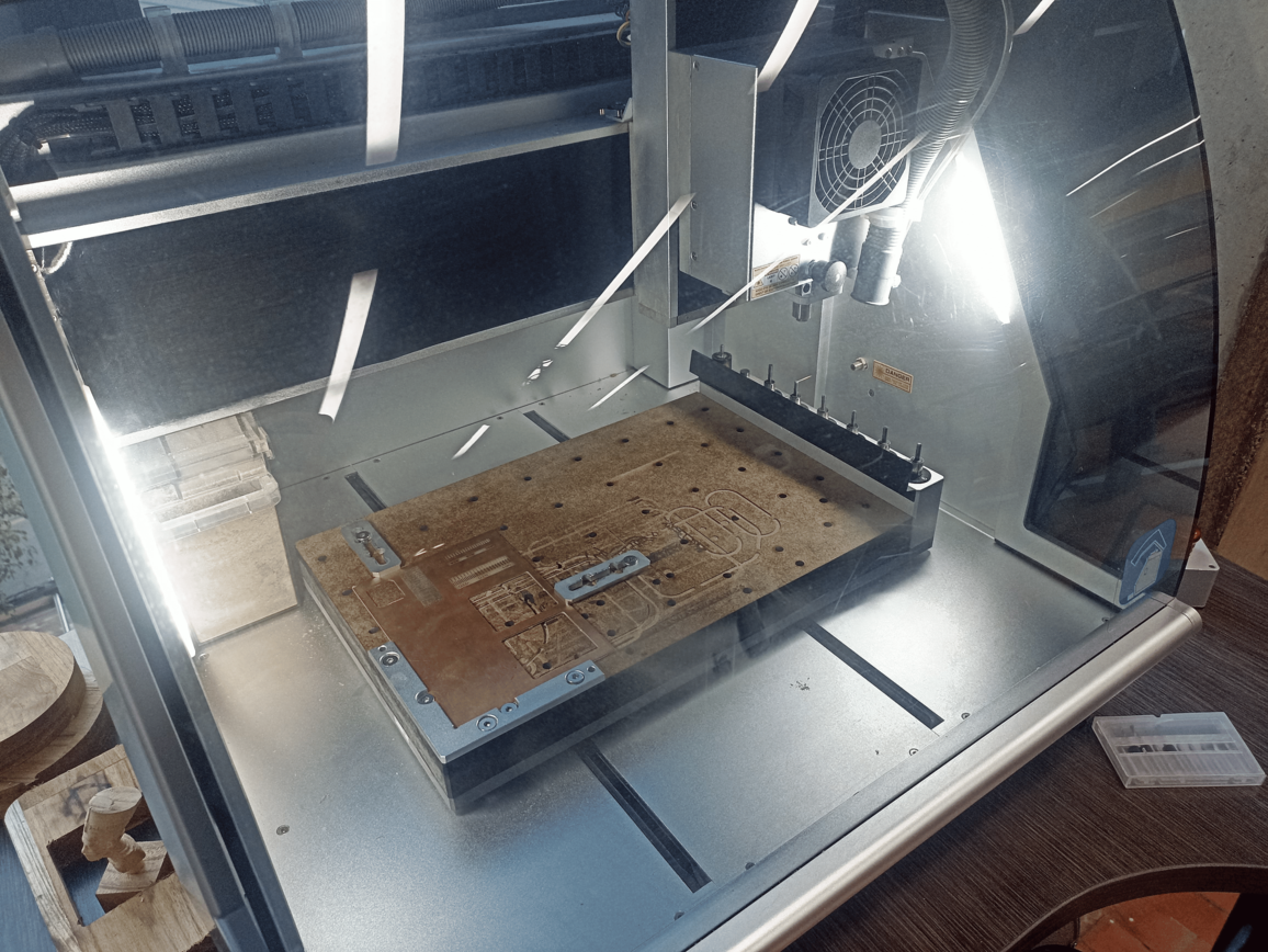
This is the Makera Carvera, the CNC router I used for board production. Compact, precise, and ideal for electronics fabrication.
Makera Carvera – Key Specs
| Feature | Specification |
|---|---|
| Build Volume | 300 × 250 × 100 mm |
| Spindle | 300W Brushless Motor |
| Tool Changer | Automatic (up to 4 tools) |
| Supported Formats | SVG, DXF, Gerber, STEP |
| Precision | ±0.01 mm (10 µm) |
| Software | Fusion 360, VCarve, LightBurn |
Learn more on the official Makera Carvera page.
4.1 Importing the Design (DXF)
I exported the PCB outline and traces from Fritzing in DXF format and then imported it into Fusion 360. I chose DXF because it maintains correct scale, whereas SVG tends to resize or shift elements when imported into Fusion.
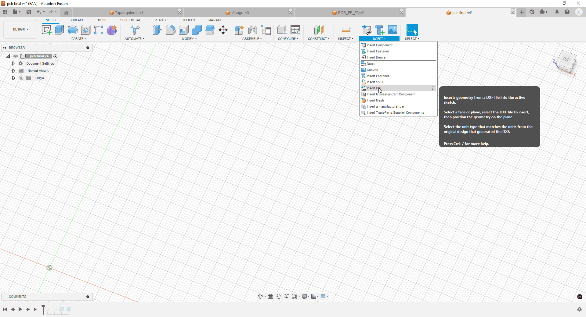
DXF import screen in Fusion 360. I carefully checked that all lines were preserved and displayed correctly.
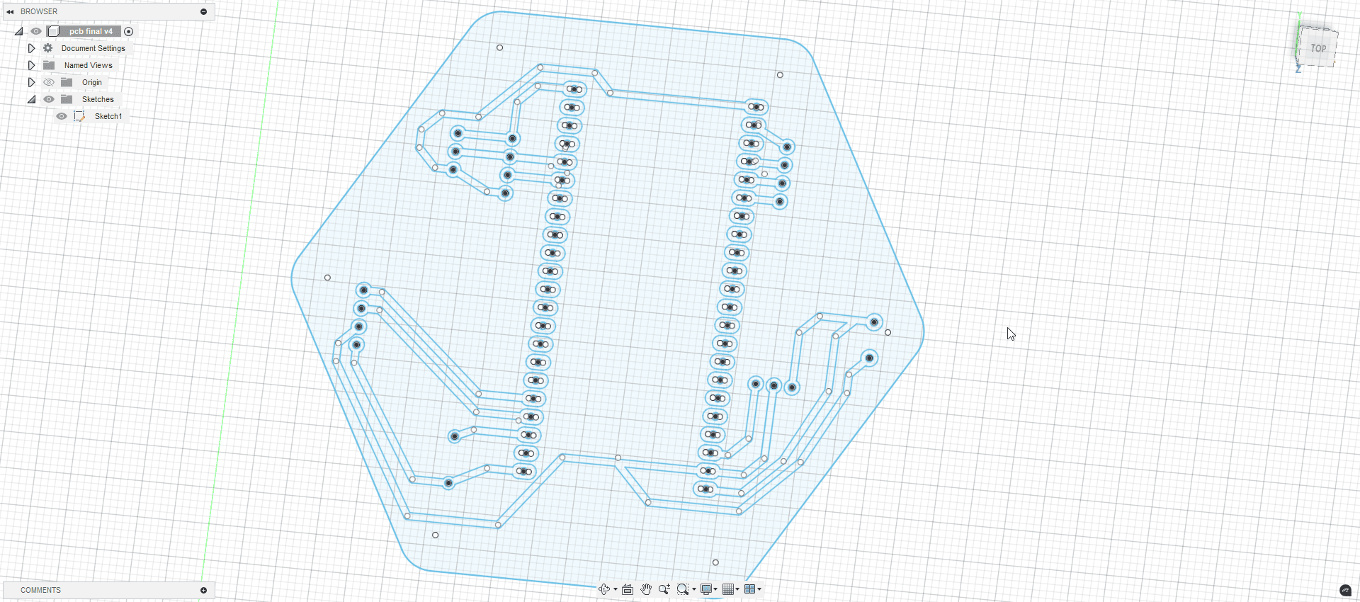
The lines and shapes imported cleanly. This verification step is essential to avoid problems during toolpath generation.
4.2 3D Modeling the PCB
While it’s possible to cut directly from 2D geometry, I wanted to mill the copper layer — so I modeled the board in 3D. First, I extruded the base plate to 1.55 mm (since the copper layer is 0.15 mm and the total PCB thickness is 1.7 mm).
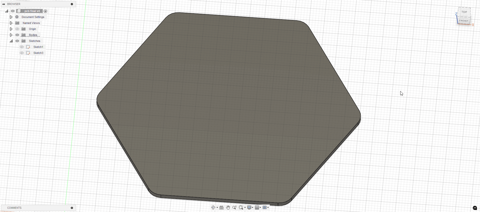
Base extrusion to 1.55 mm. This accounts for copper thickness that will be removed in the milling process.
I selected the copper traces and extruded them by 0.15 mm to represent the full board in 3D.
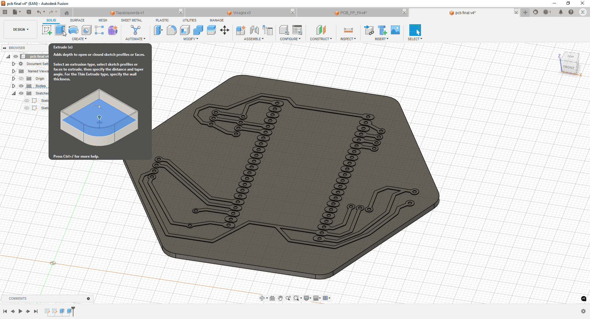
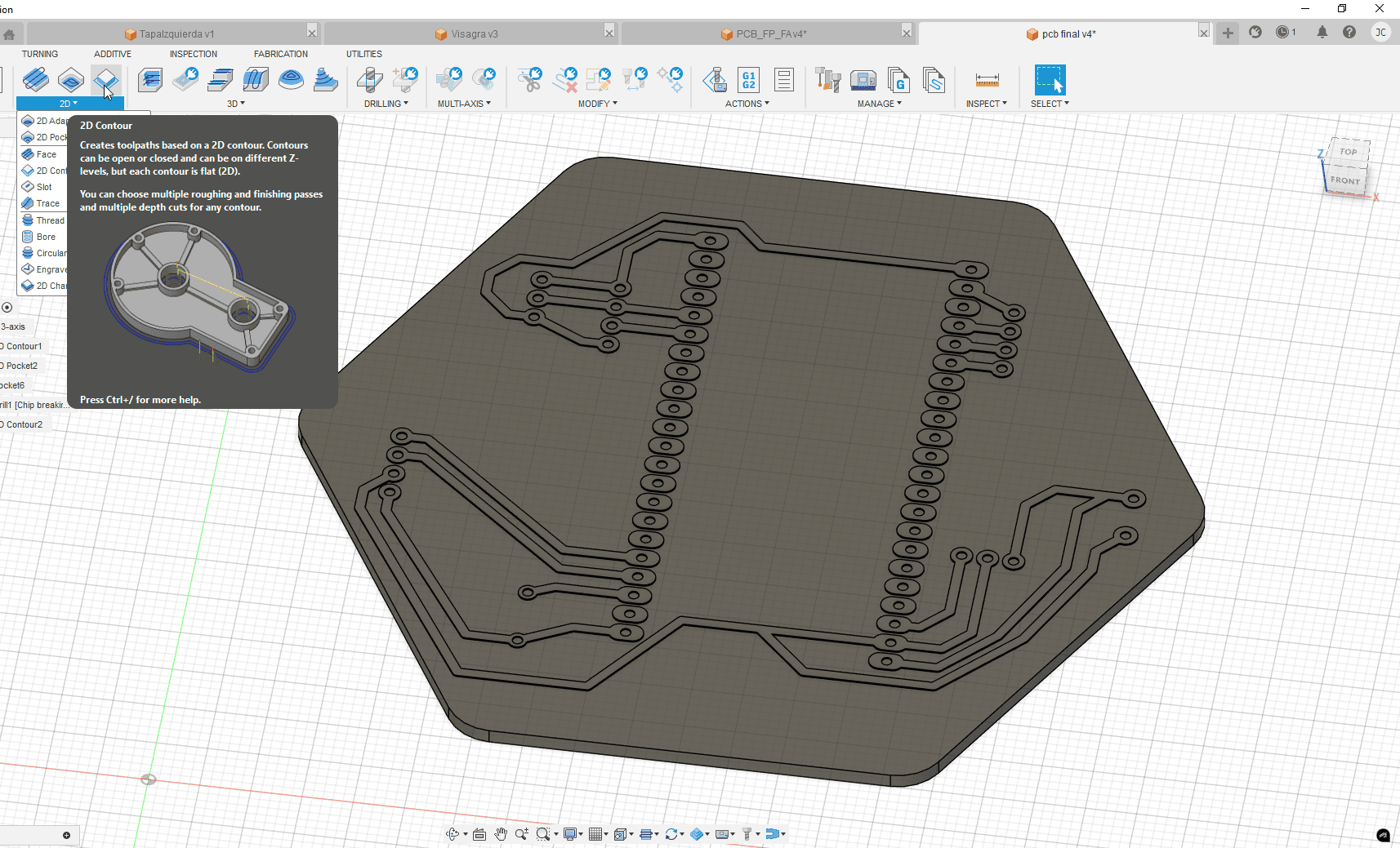
4.3 CAM Strategy
To set up the CAM operations, I switched from the Design workspace to the Manufacture tab in Fusion 360. From there, I defined the operations in the following order, which we validated during group work as a safe and effective workflow:
- Pocket: to remove copper between traces and isolate signal paths.
- Cleanup contour: to remove any excess material from the board's interior.
- Drill: for component holes and via placements.
- 2D Contour: to cut out the entire PCB shape and outline.
4.4 Material Stock and Origin
The first step in the CAM setup was to define the stock material and the origin point. I used the full size of the copper-clad PCB I planned to machine, and set the origin at the bottom-left corner to align with the machine's reference.
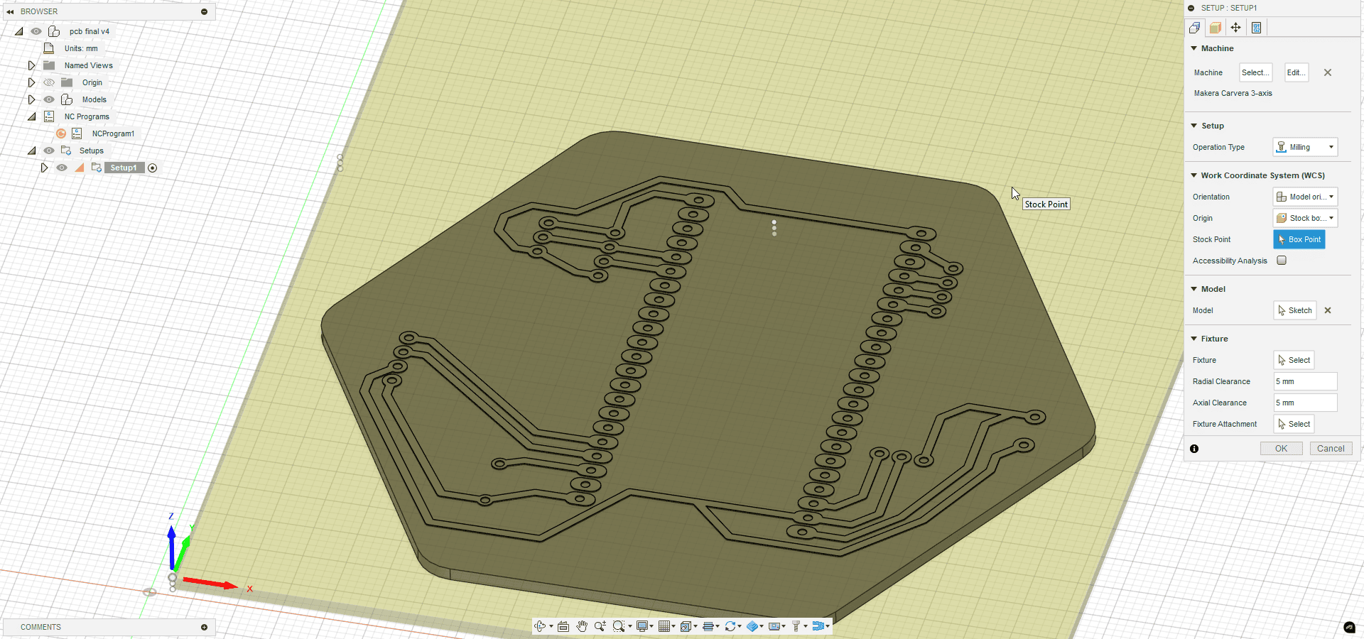
Stock size and origin setup inside Fusion 360.
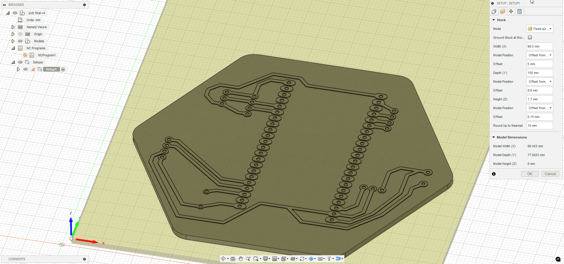
I defined the full sheet of copper board as my stock material.
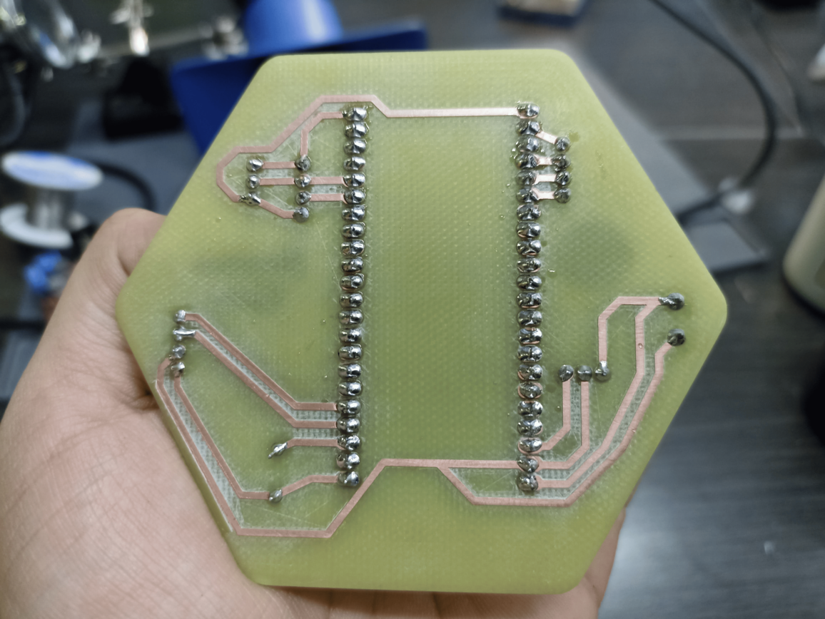
4.5 Trace Isolation with V-bit
For trace isolation, I used a 2D contour operation with a V-bit tool, which is ideal for precisely carving around signal lines. The V-shape allows clean cuts with minimal tool pressure and great detail.
I selected the 2D contour operation for isolating all traces.
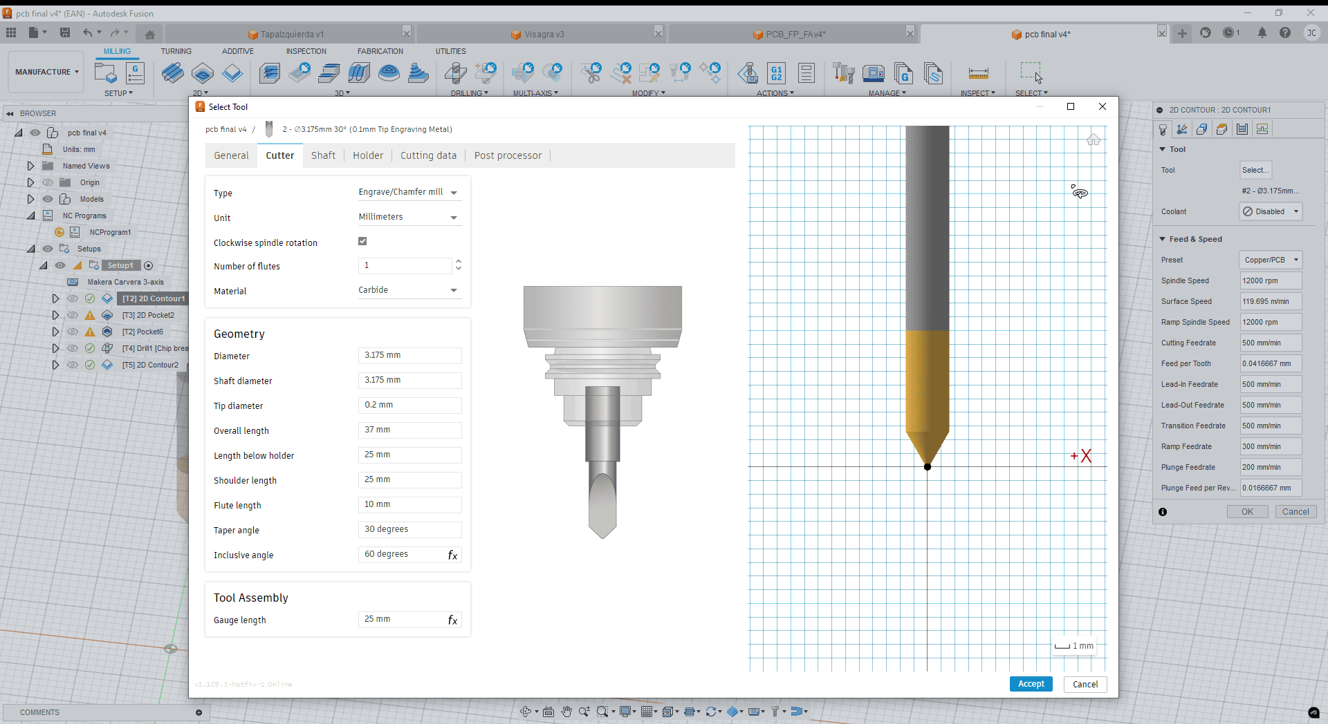
Configured T2: a sharp V-bit for precision milling of signal lines.
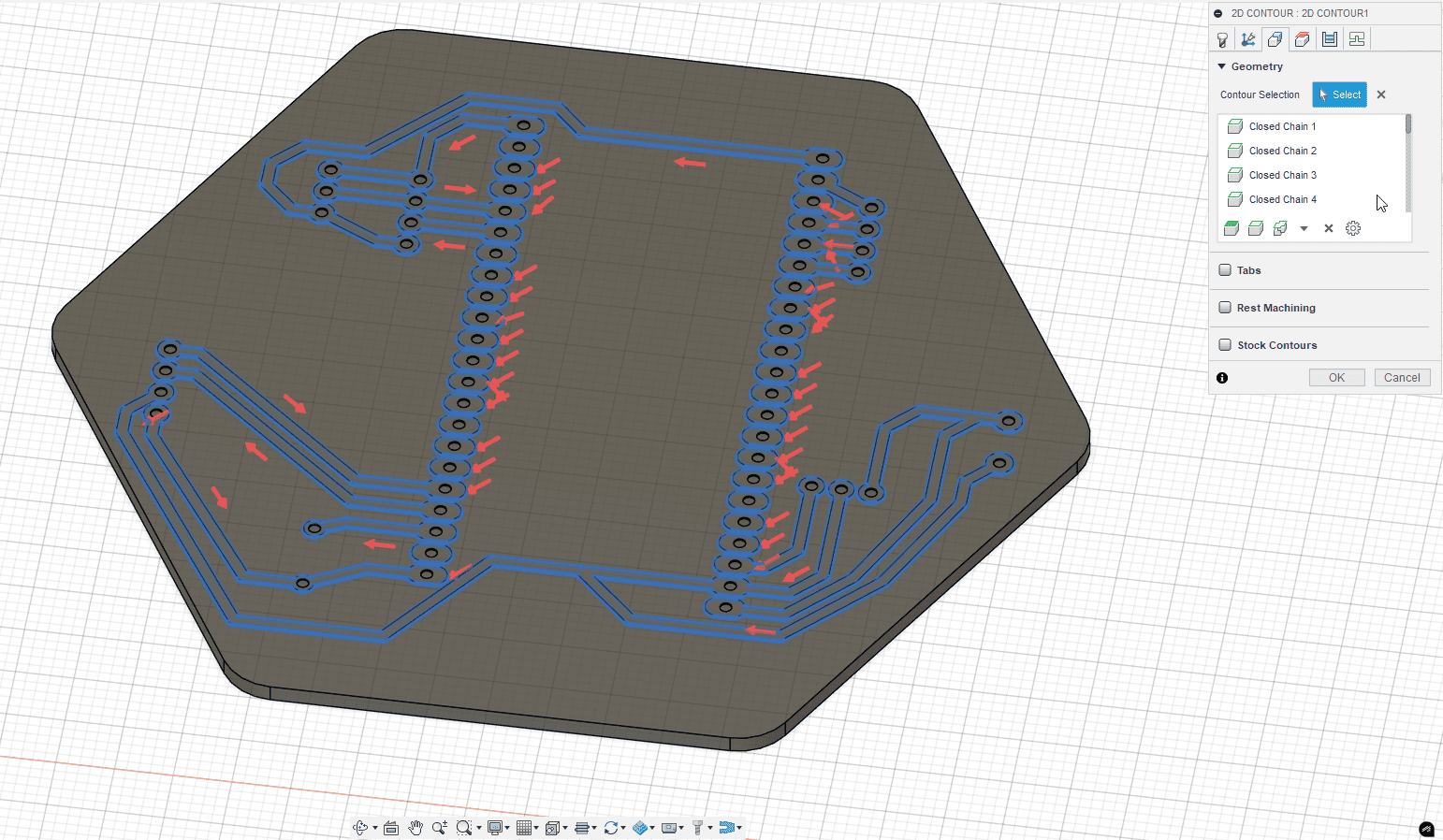
All trace contours were selected manually for better control.
Final toolpath settings: 0.15 mm cutting depth, reduced ramp speeds, and gentle engagement to preserve tool quality.
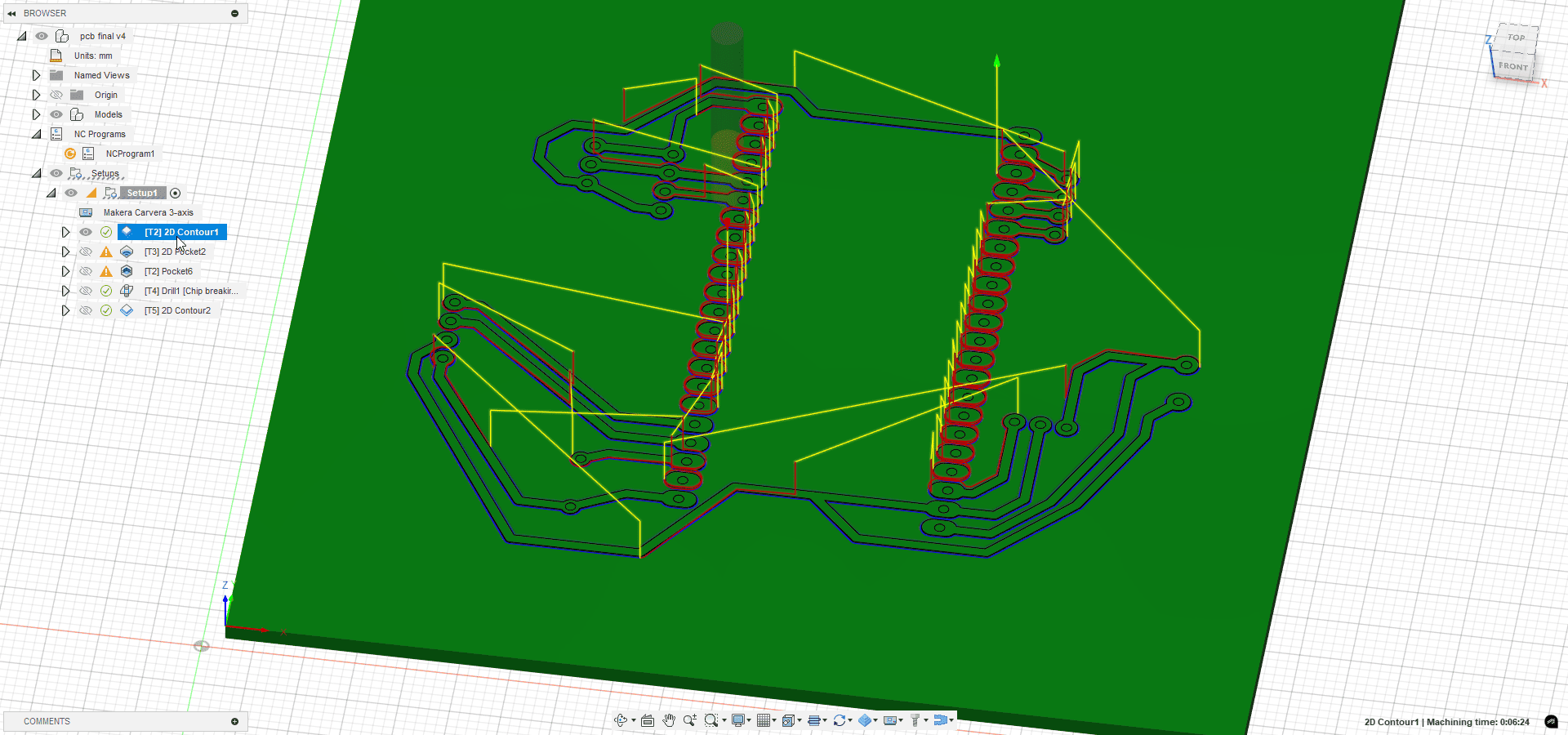
The toolpath shows clean isolation around every trace.
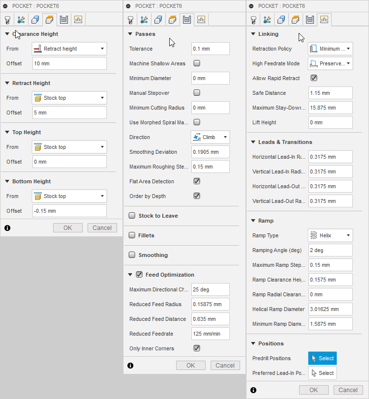
4.6 Copper Removal with 2D and 3D Pocket
To remove the rest of the copper, I used two types of pocket operations. First, I defined a standard 2D Pocket using a flat endmill (T3). This allowed me to remove large areas efficiently without touching the traces.
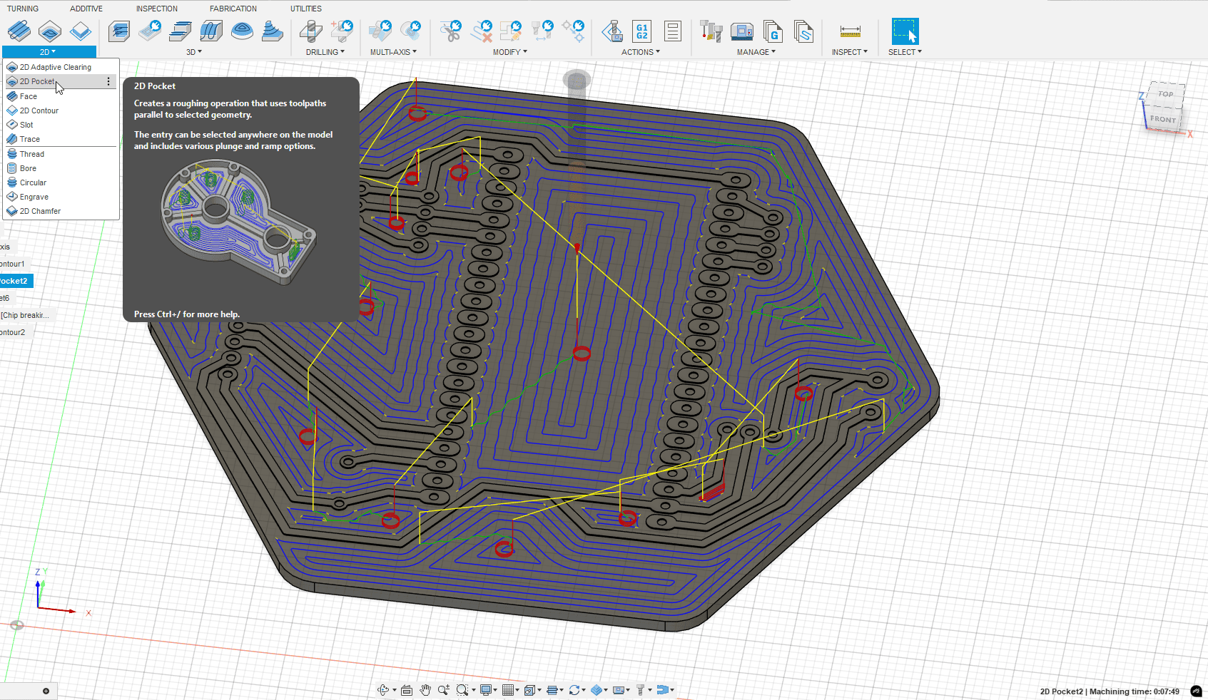
Initial copper removal was done using a 2D pocket operation.
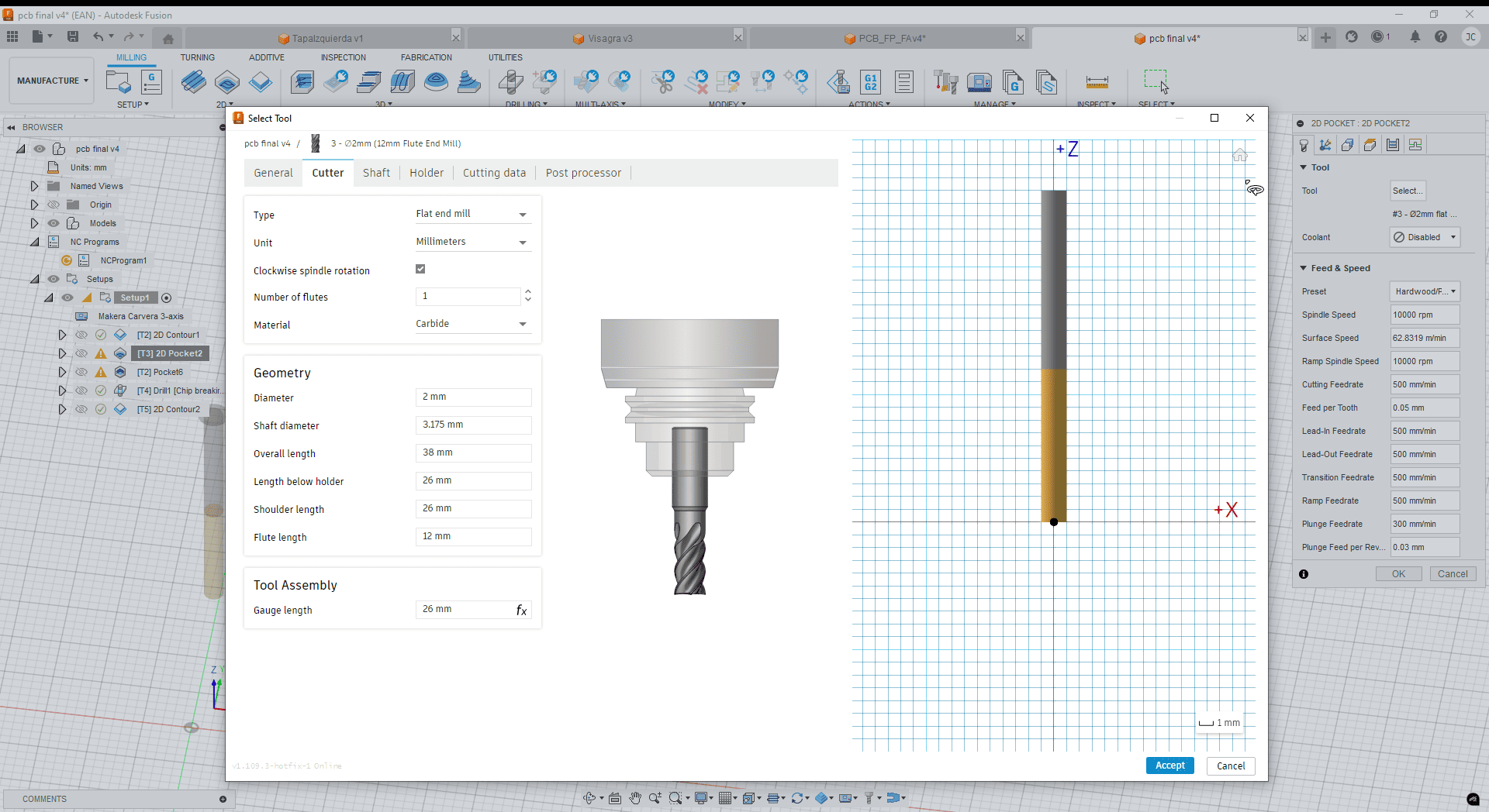
Tool T3: a flat-end mill ideal for copper clearing.
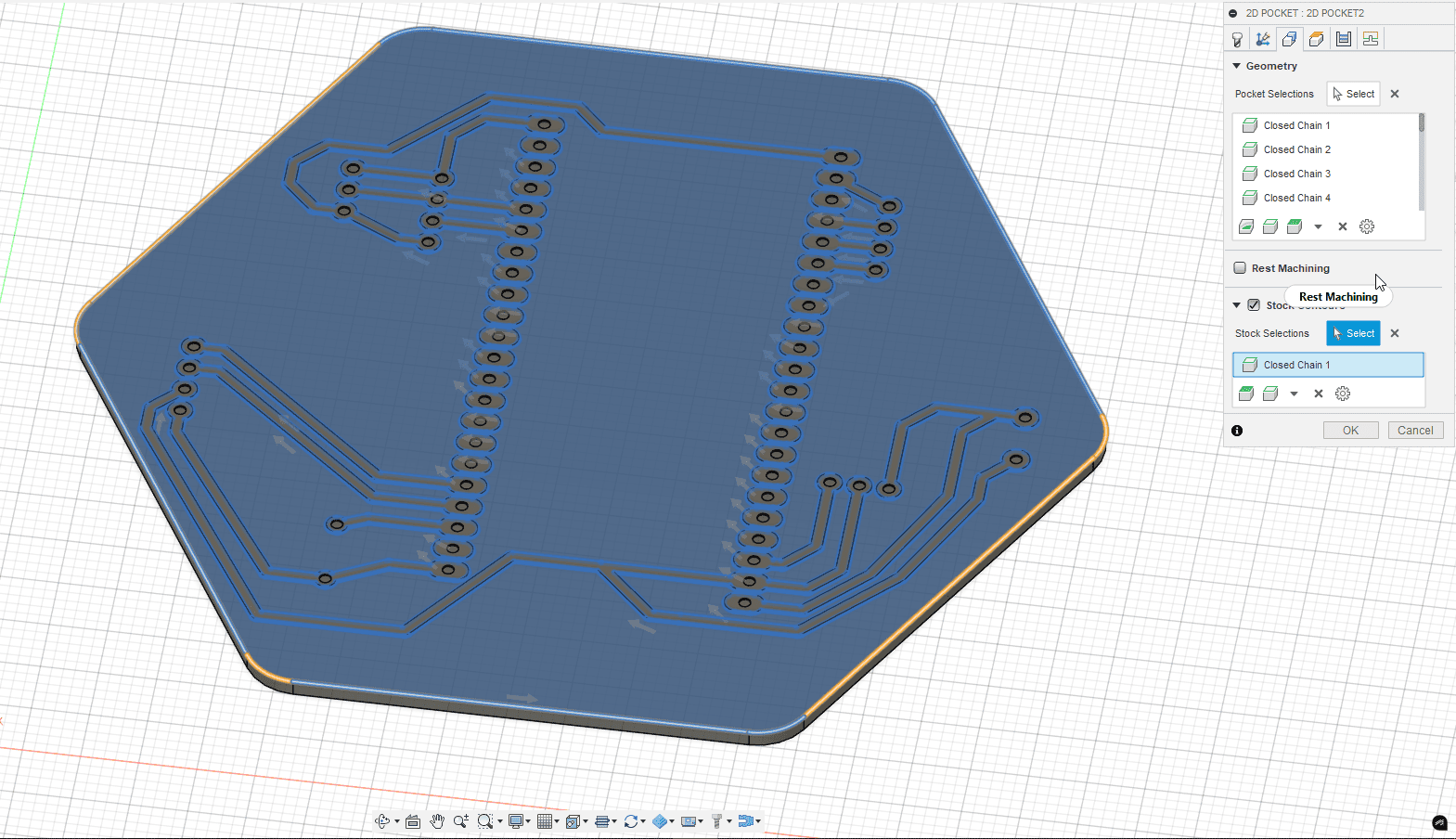
I selected the areas between traces and added a bounding border to avoid spills.
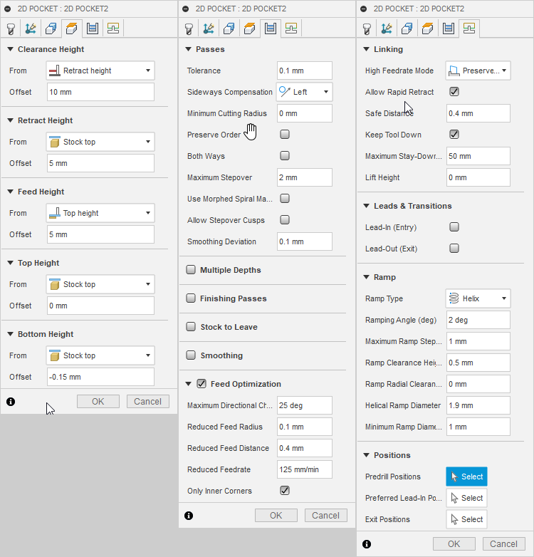
Default tool library values were used, adjusting heights, passes, and linking tabs.
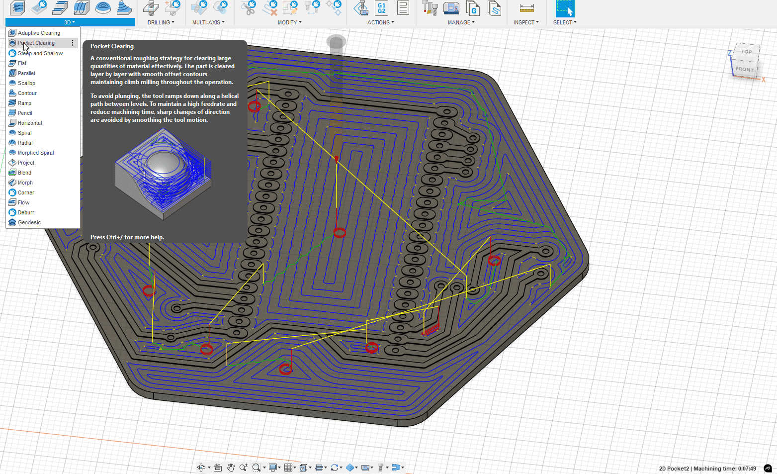
To clean up fine corners the 2D pocket couldn’t reach, I used a 3D Pocket operation with the V-bit again. This balanced time and detail.
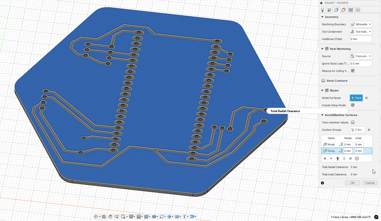
Surface selection for the second pass, targeting leftover copper details.
4.7 Drilling Holes
For drilling, I used the Drill operation to partially open all required holes on the PCB. This method is one of the fastest and most efficient ways to prepare components' holes with precision.
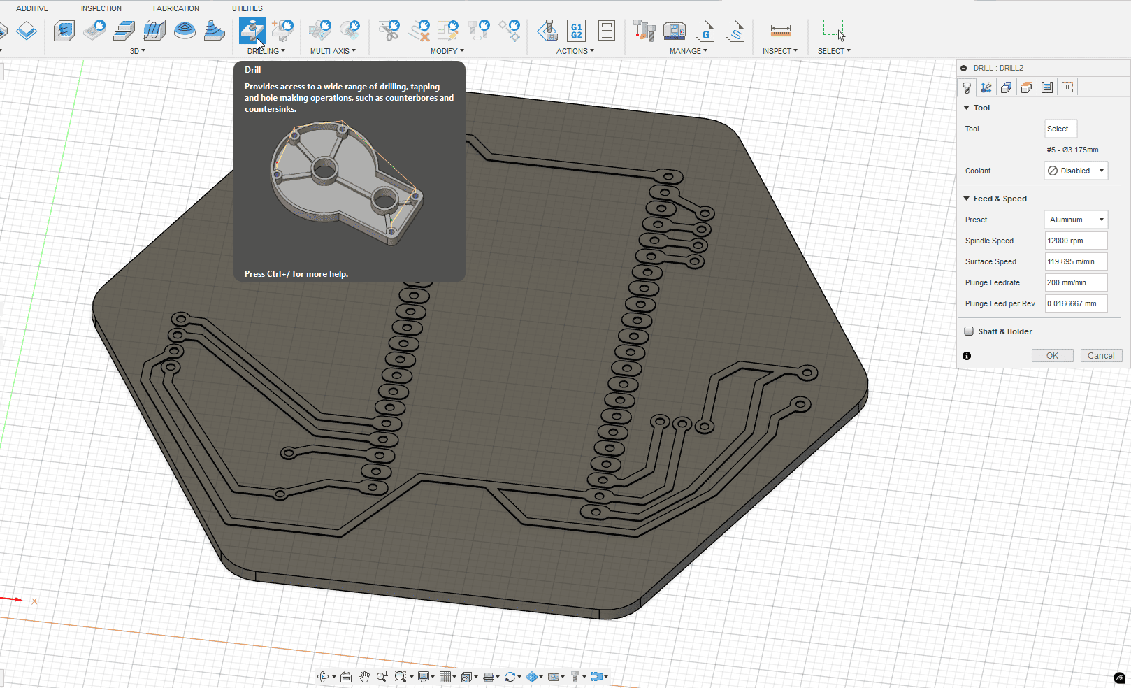
Drill selected in the CAM environment.
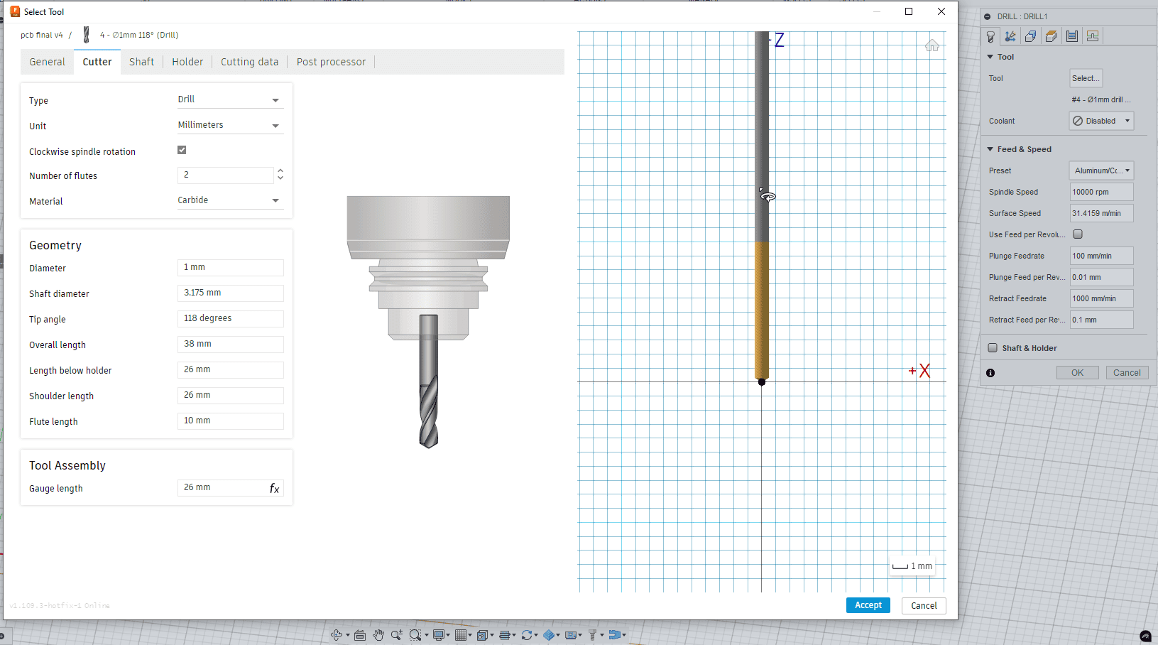
Tool T4: 1mm diameter drill bit for precision holes.
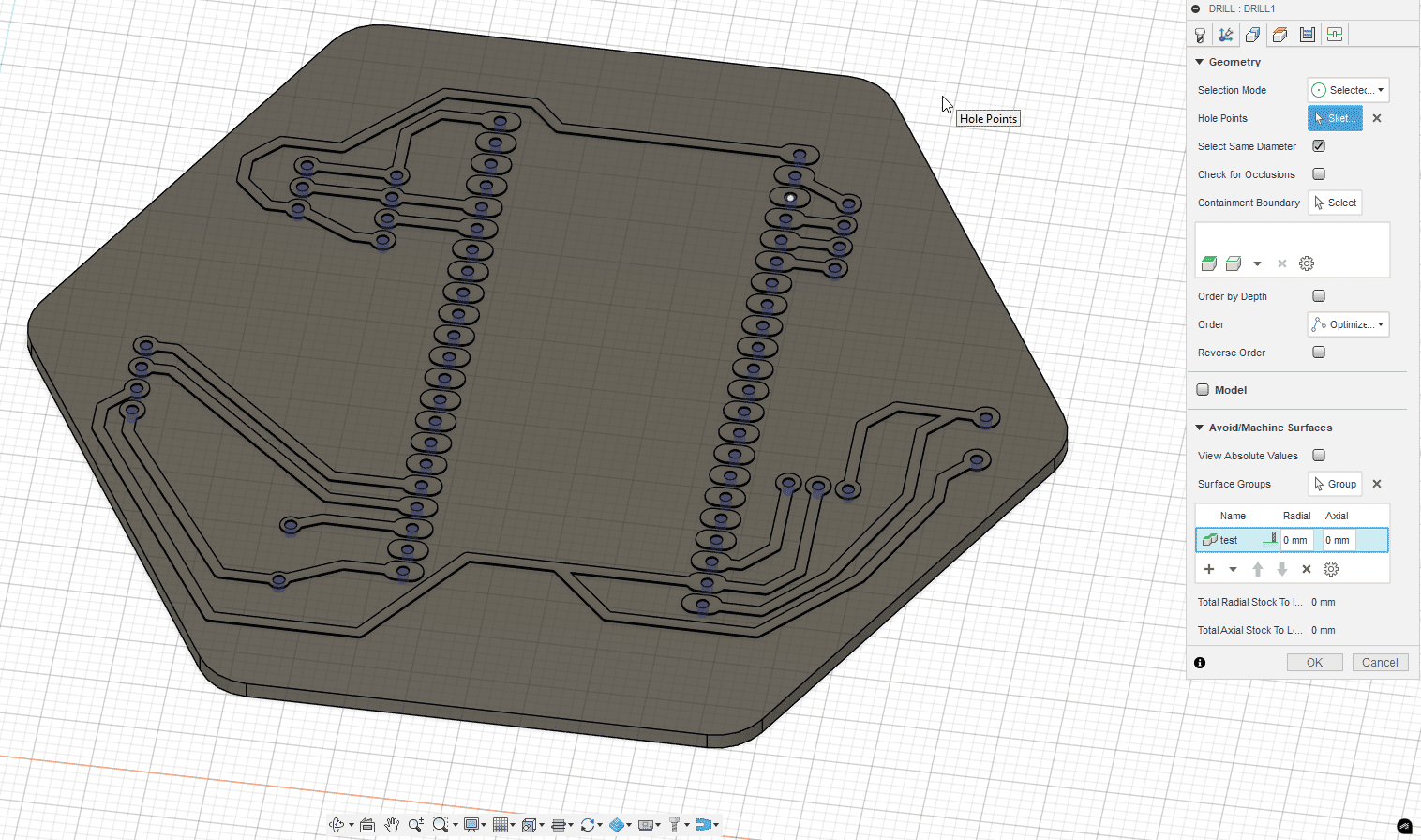
Some holes required manual selection — an easy process within the 3D view.
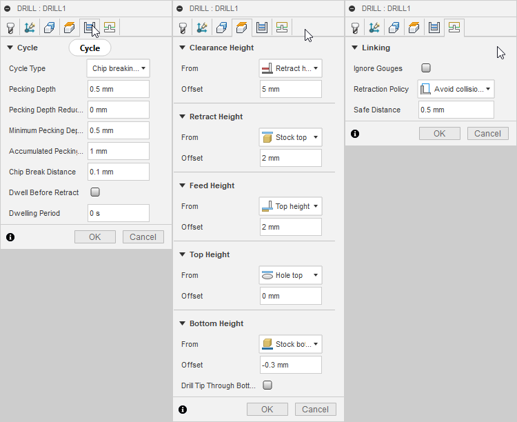
Height control and linking settings for partial hole depth.
4.8 Cutting PCB Contours
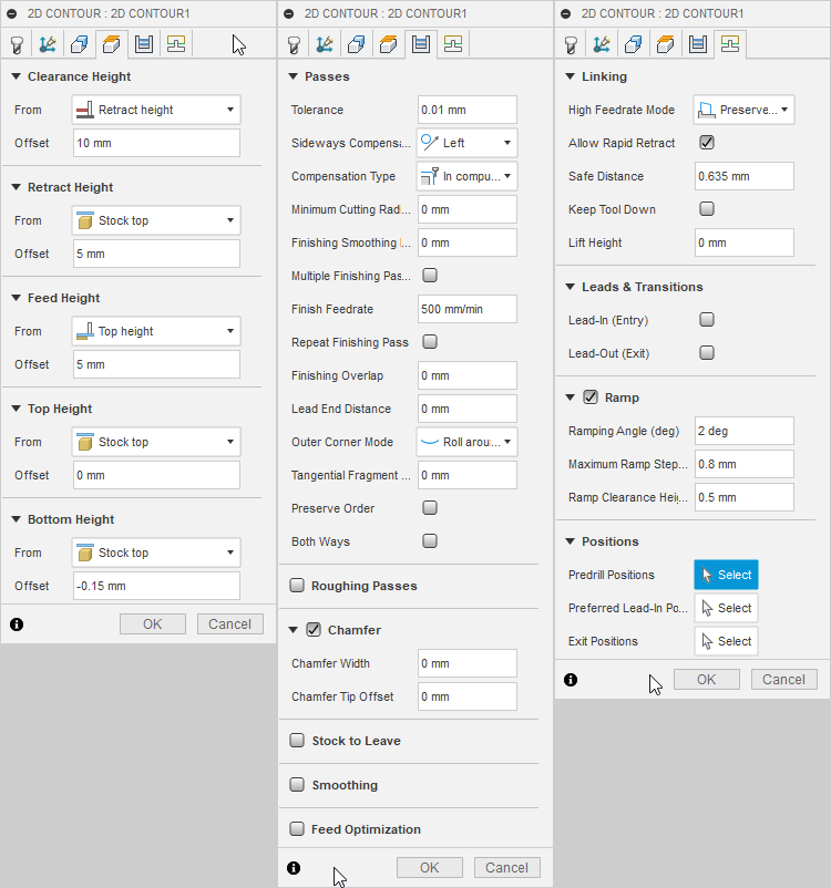
For the final cutout, I reused the 2D Contour operation with the flat tool (2mm diameter). I configured the operation to include tabs, which are essential to keep the piece attached to the material and prevent damage to the tool or the job.
To ensure the cut goes fully through, I adjusted the depth slightly beyond the material thickness by -0.2 mm. Since we added an MDF sacrificial layer, this doesn’t pose a risk to the machine.
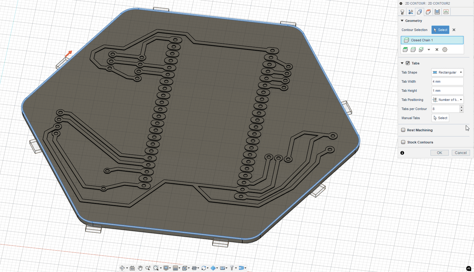
I enabled tabs and selected the board outline to keep the part fixed during cutting.
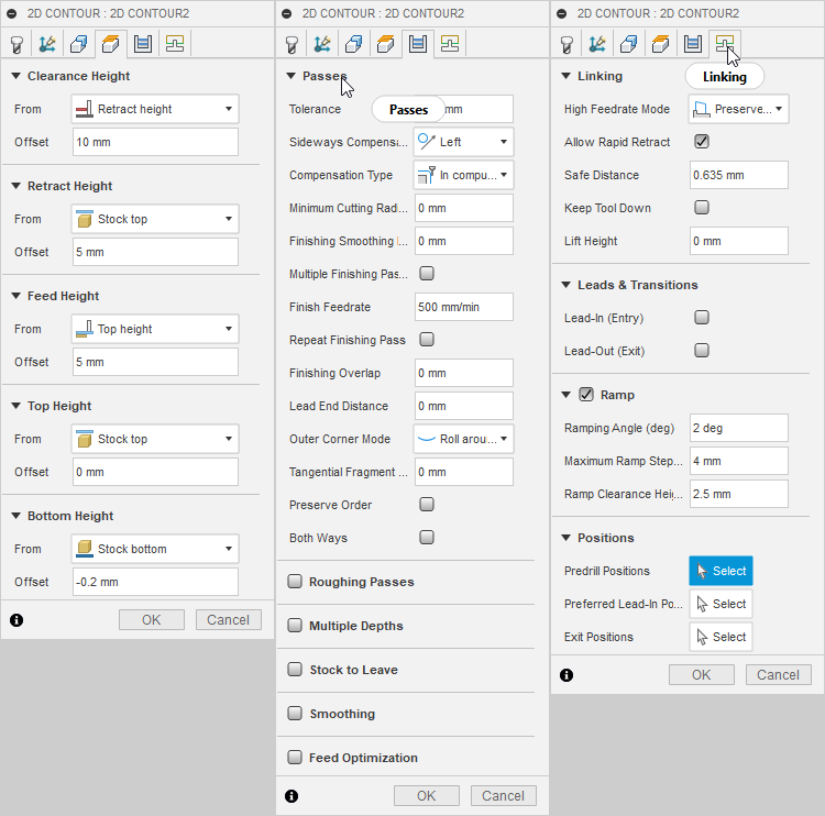
All heights, passes, and safety ramp options were configured correctly.
4.9 CAM Simulation
Once all five operations were defined, I reviewed the complete toolpath. Fusion 360 allows simulation of the entire process to visualize and verify tool movement.
- Trace contour
- Copper removal – pocket roughing
- Copper cleanup – fine pass
- Hole drilling
- Final board cutout
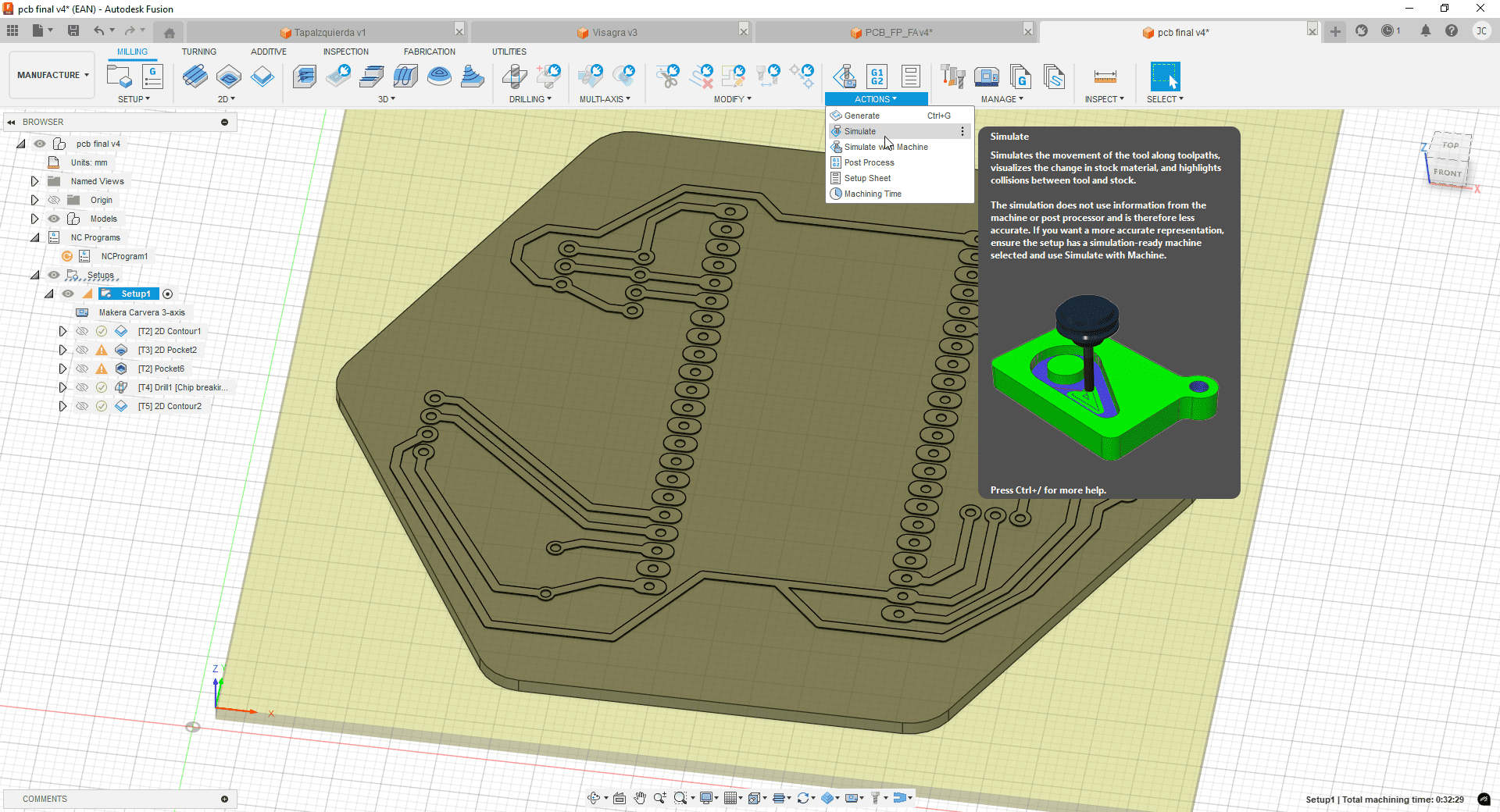
Fusion 360 simulation view to verify safe tool movements.
4.10 G-Code Generation
With all operations ready, I selected the setup (which includes the stock and origin) and used the Post Process option in Fusion 360 to generate the G-code.
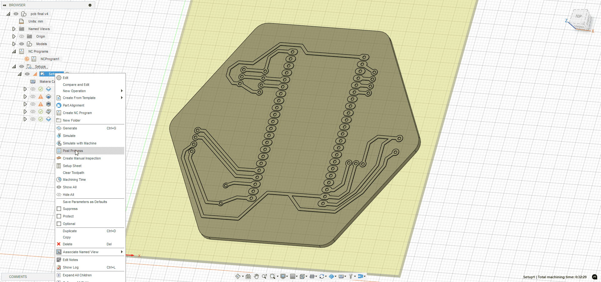
Post processor ready with all required configuration options.
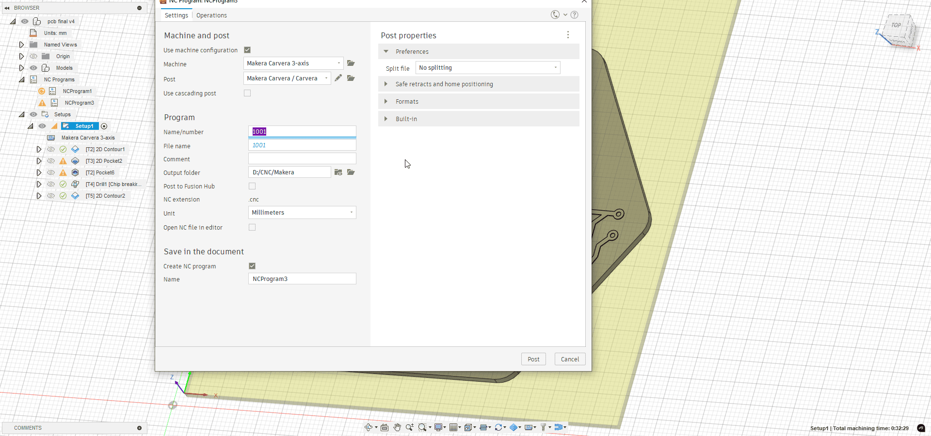
I selected the right post, output folder, file name, and generated the machine code.
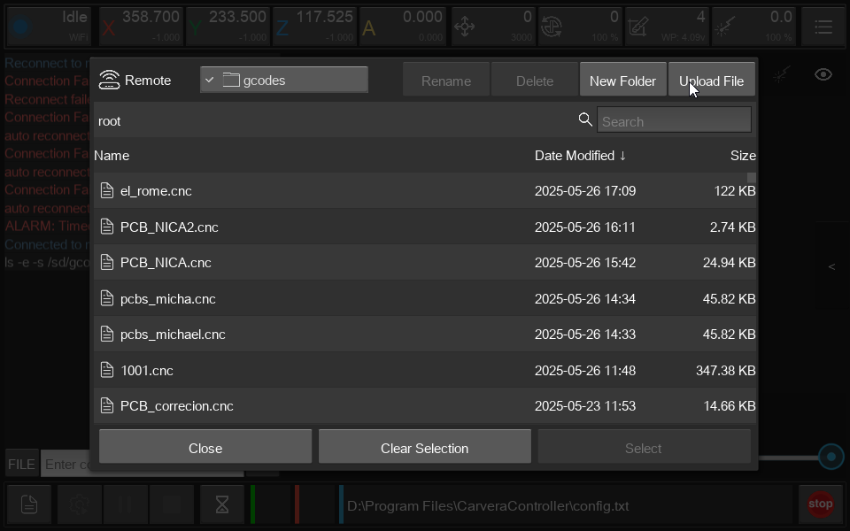
4.11 Carvera Controller Setup
The G-code was uploaded to the Carvera CNC machine using its dedicated controller software: Carvera Controller. After turning on the machine and connecting via Wi-Fi, I loaded the .gcode file.
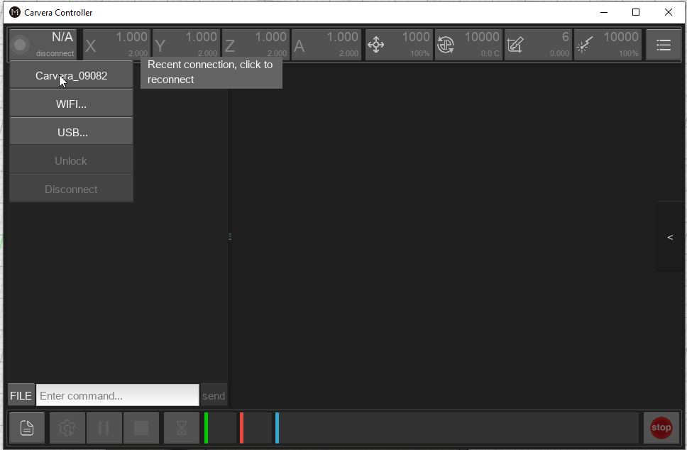
Machine turned on and recognized by the software.
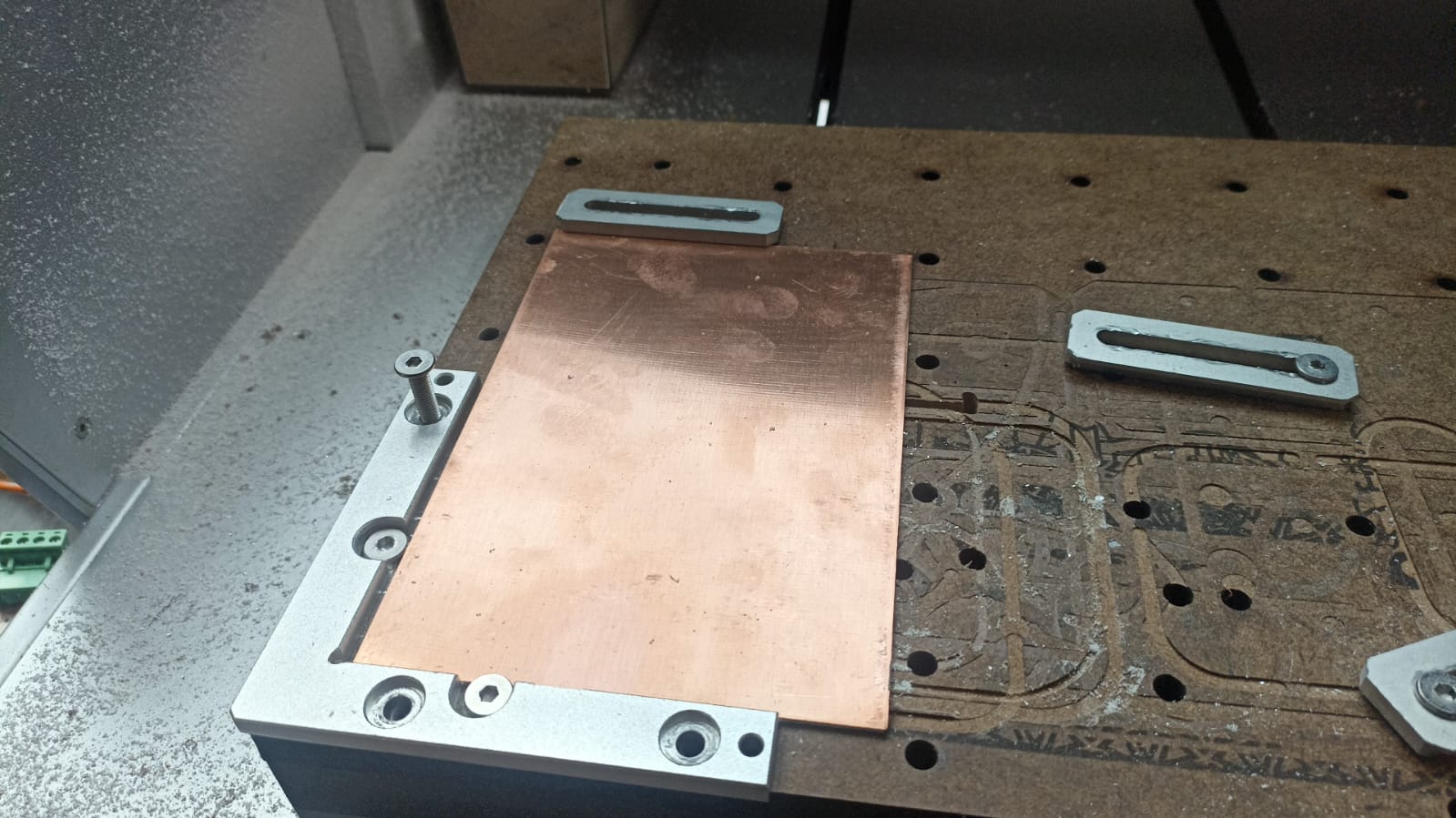
The board was mounted securely, with tools checked and aligned as in the CAM setup.
Loading and reviewing the job before sending it to the machine.
Enabling mesh leveling, margin probing, and setting material height before starting.
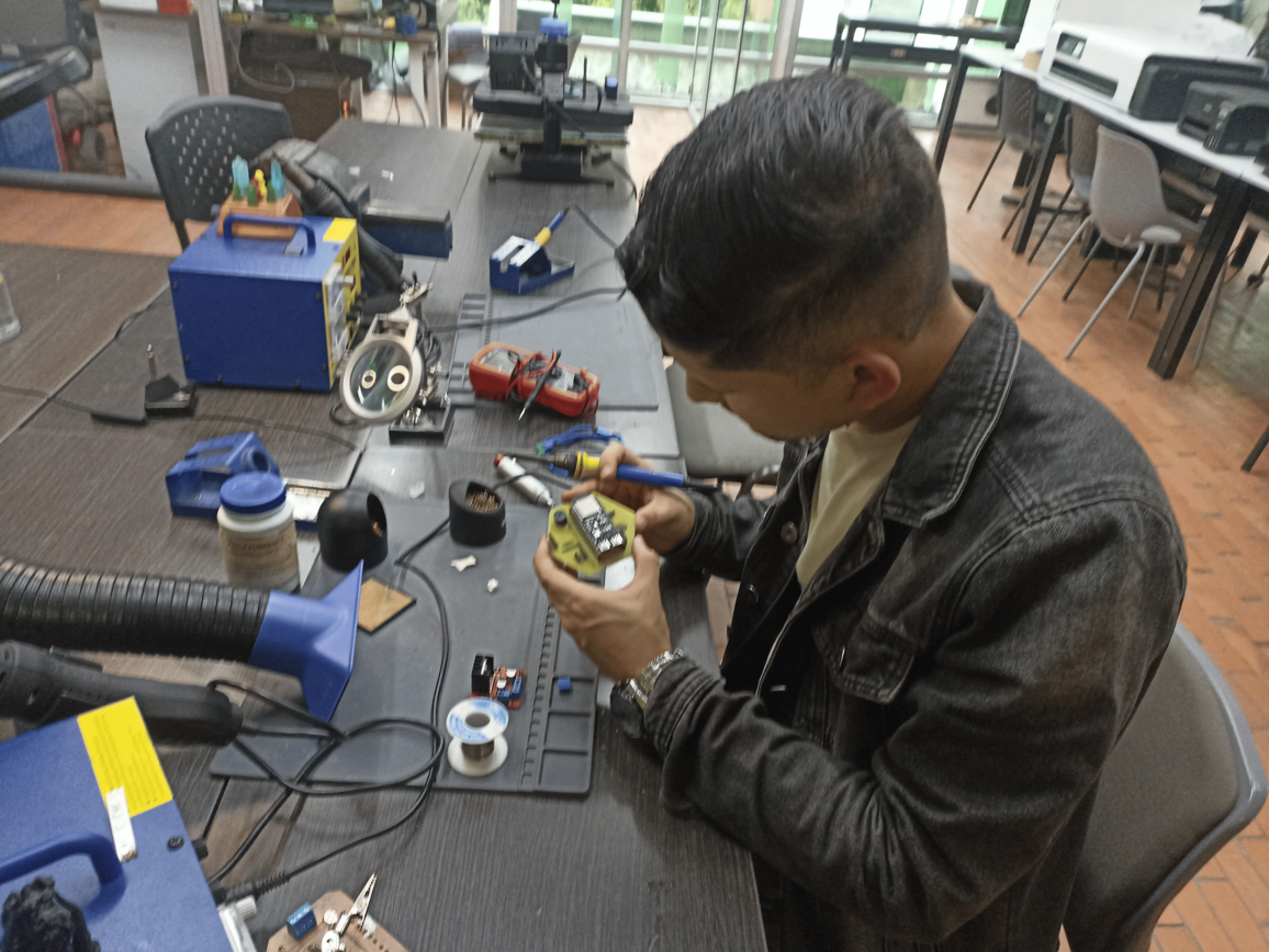
5). Board Finishing and Assembly
5.1 Sanding and Cleaning
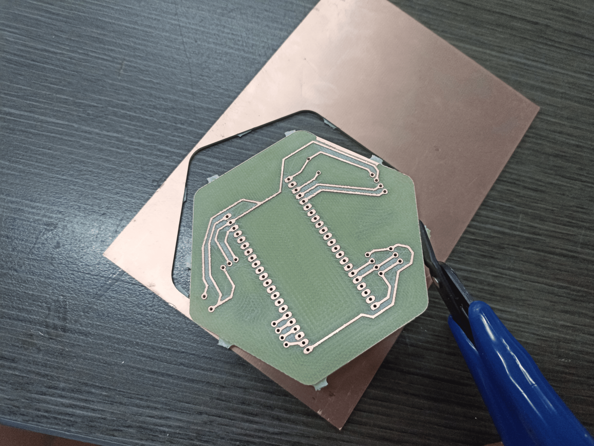
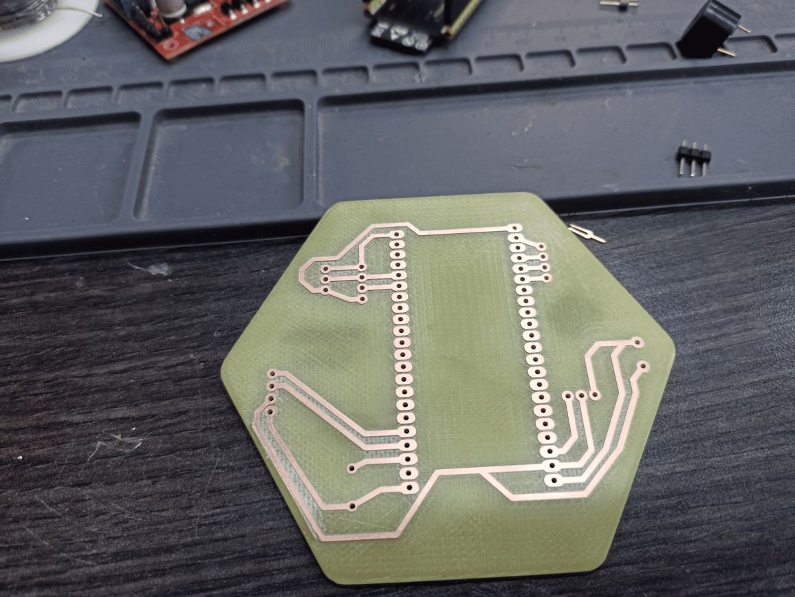
Once the board was cut, I manually removed the tabs that held the PCB to the copper sheet. Then, I lightly sanded the edges using fine sandpaper to eliminate any remaining burrs or debris left after milling.
5.2 Visual and Electrical Inspection
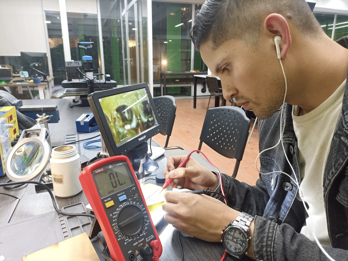
Before soldering, I performed a careful inspection to ensure no traces were shorted or unintentionally connected. I used a multimeter in continuity mode and a digital microscope to verify every detail of the circuit.
5.3 Soldering
Once the inspection was complete, I soldered the main components: headers for the ESP32-S3, a buzzer, and a power terminal block. I followed standard soldering practices to ensure secure and clean joints.
6). Testing
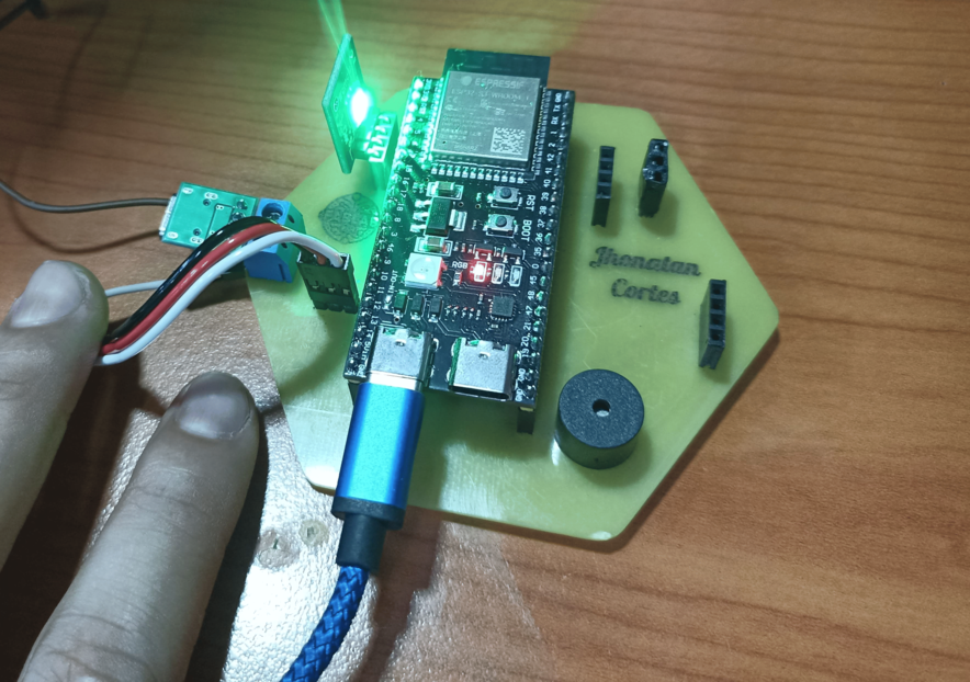
6.1 Power-On Test
After assembling the board, I inserted the ESP32-S3 without connecting any peripherals and powered it via USB. Once I confirmed that the board was functioning without issues, I connected an RGB LED to perform a basic lighting test. Everything worked perfectly.
ESP32-S3 RGB Test Code
Use this code to test your capacitive RGB LED connected to pins 4, 5, and 6:
#define GREEN_PIN 4
#define RED_PIN   5
#define BLUE_PIN  6

void setup() {
  pinMode(GREEN_PIN, OUTPUT);
  pinMode(RED_PIN, OUTPUT);
  pinMode(BLUE_PIN, OUTPUT);

  digitalWrite(GREEN_PIN, HIGH);
  digitalWrite(RED_PIN, HIGH);
  digitalWrite(BLUE_PIN, HIGH);
}

void loop() {
  digitalWrite(GREEN_PIN, LOW);
  digitalWrite(RED_PIN, HIGH);
  digitalWrite(BLUE_PIN, HIGH);
  delay(2000);

  digitalWrite(GREEN_PIN, HIGH);
  digitalWrite(RED_PIN, LOW);
  digitalWrite(BLUE_PIN, HIGH);
  delay(2000);

  digitalWrite(GREEN_PIN, HIGH);
  digitalWrite(RED_PIN, HIGH);
  digitalWrite(BLUE_PIN, LOW);
  delay(2000);

  digitalWrite(GREEN_PIN, LOW);
  digitalWrite(RED_PIN, LOW);
  digitalWrite(BLUE_PIN, HIGH);
  delay(2000);

  digitalWrite(GREEN_PIN, LOW);
  digitalWrite(RED_PIN, HIGH);
  digitalWrite(BLUE_PIN, LOW);
  delay(2000);

  digitalWrite(GREEN_PIN, HIGH);
  digitalWrite(RED_PIN, LOW);
  digitalWrite(BLUE_PIN, LOW);
  delay(2000);

  digitalWrite(GREEN_PIN, LOW);
  digitalWrite(RED_PIN, LOW);
  digitalWrite(BLUE_PIN, LOW);
  delay(2000);

  digitalWrite(GREEN_PIN, HIGH);
  digitalWrite(RED_PIN, HIGH);
  digitalWrite(BLUE_PIN, HIGH);
  delay(2000);
}
7). Problems and Learnings
One of the main issues I detected during the group assignment was that some EDA tools don’t always define hole distances properly. Because of this, I made sure to validate the layout before cutting the final board. I even ran a drilling test on a scrap PCB.
Another common mistake involves not using tabs during contouring. I avoided this issue by enabling them early on. Additionally, I’ve learned to monitor the machine closely, as some collets may not fully tighten, causing tools to slip or the machine to pause unexpectedly. This time, I had no issues — but I’ve experienced them in previous jobs.
During the fabrication of my final PCB, I didn’t encounter any problems or errors. The process went smoothly from start to finish. Although I hadn’t tested this exact board design before, I conducted multiple preparation tests using other boards and materials — including one specifically to validate the mechanical fit of the ESP32-S3 module footprint.
For the CNC milling process, I was already familiar with the machine’s tolerances — for example, the minimum trace clearance of 0.15mm — and I applied this knowledge to define the toolpaths, depths, and speeds carefully.
I also carried out some preliminary experiments using a fiber laser on other test materials, which helped me understand how different methods affect cut quality and resolution.
Thanks to all this testing and planning, the final PCB fabrication and soldering stages were successful. I was precise and patient while assembling components, and no errors such as shorts or misalignments occurred. This project reinforced the value of preparing carefully, validating assumptions, and applying lessons from earlier assignments.
Personal Reflections and Conclusions
This week was especially valuable for reinforcing my understanding of CNC machines and the full PCB production process. Although I’ve used this machine before, I still consider myself in training. This assignment pushed me to explore everything — from digital design to physical manufacturing — and do it cautiously to avoid mistakes.
I realized how important PCBs are for turning prototypes into reliable products. Unlike messy breadboards with fragile wiring, a good PCB layout offers structure, clarity, and stability. I didn’t make any significant mistakes this time, mostly because I was cautious, reviewed previous work from my peers, and applied what I learned from group sessions.