Assignments
Group Assignment:
- Use the test equipment in your lab to observe the operation of a microcontroller
circuit board (as a minimum, you should demonstrate the use of a multimeter and
oscilloscope).
- Document your work on the group work page and reflect what you learned on your
individual page.
Individual Assignment:
- Use an EDA tool to design a development board that uses parts from the inventory
to interact and communicate with an embedded microcontroller.
Week 6. Electronics Design
Reflection on Group Work and Personal Learning
As part of the group assignment, we used lab equipment to evaluate the behavior of a microcontroller development board. I worked with the ESP32-S3 DevKitC-1, focusing on a basic digital output test using an RGB LED.
I uploaded a simple program to blink the red channel of the RGB LED. Using a multimeter, I confirmed that the GPIO pin toggled between 0V and 3.3V, which corresponded to the ON and OFF states of the LED. Then, I used an oscilloscope to visualize the PWM signal generated by the ESP32-S3. This allowed me to observe the duty cycle and frequency in real time, validating the correct configuration of the timer and pin setup.
The oscilloscope showed a clean square wave during the blinking sequence, matching the expected HIGH and LOW timing. This confirmed that the board was executing the program properly, and that the hardware was stable and responsive.
This activity helped me reinforce the relationship between software configuration and real-time signal behavior, and how to validate digital outputs using both basic and advanced lab tools.
1). Introduction
This week focused on the process of designing a PCB (Printed Circuit
Board) using an EDA (Electronic Design Automation) tool.
Personally, I had limited prior experience with PCB design, so I approached this week
with caution and curiosity.
I began by researching various design tools to identify which ones were
beginner-friendly and best suited for this assignment.
After evaluating several options, I chose Fritzing for its intuitive
interface and ease of use — especially valuable for those just starting out in circuit
design.
I then explored tutorials and documentation to understand how to transition from a
breadboard-style circuit to a schematic and finally to a PCB layout.
This process helped me not only design my own board but also learn key concepts about
logical connections, track routing, and file generation for fabrication.
In the following sections, I’ll describe the step-by-step workflow I followed and the
considerations I took into account during the design process.
2). Comparative Analysis of PCB Design Tools
🔧 Tool Overview
- Fritzing – Beginner-friendly, drag-and-drop interface, excellent for early prototyping and educational use.
- EasyEDA – Web-based, integrates component libraries and PCB manufacturing, easy to access from anywhere.
- KiCad – Free and open-source, offers advanced features like 3D visualization, hierarchical schematics, and DRC checks.
- Eagle – Industry-level tool from Autodesk, includes advanced autorouting, component libraries, and commercial integration (Fusion 360).
📝 Key Comparison
| Tool | Difficulty | Main Features | Best For |
|---|---|---|---|
| Fritzing | ⭐ Very Easy | Visual design, schematic & PCB views | Beginners, students |
| EasyEDA | ⭐ Easy | Online editor, built-in ordering | Hobbyists, rapid prototyping |
| KiCad | ⭐⭐ Medium | DRC, 3D viewer, hierarchical design | Advanced users, open-source advocates |
| Eagle | ⭐⭐ Medium | Autodesk ecosystem, rich libraries | Professionals, Fusion 360 users |
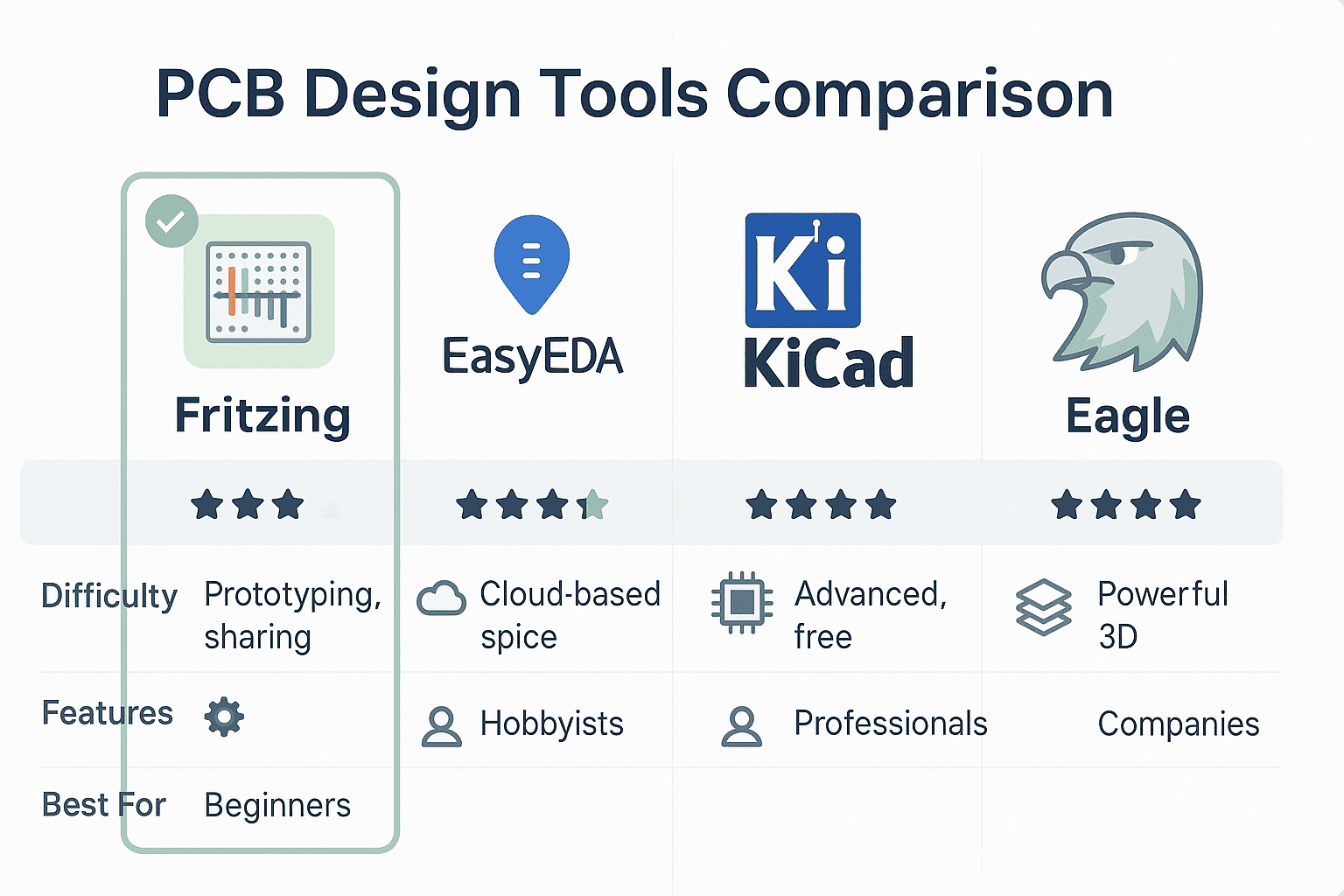
✅ My Choice: Fritzing
I selected Fritzing as my PCB design tool for this week due to its approachable interface and helpful visual model. As someone who is still learning PCB layout, I found Fritzing ideal for understanding how components relate both physically and logically. Its three-view system (protoboard, schematic, and PCB) helped me visualize the evolution of my circuit and made it easier to understand design flow.
3). Project Definition
For this week’s assignment, I decided to create a custom PCB expansion board that can support different sensors and actuators during future experiments with my ESP32-S3. The goal is to design something reusable that allows fast connection, testing, and removal of components — without having to solder everything each time.
The board will feature labeled header pin arrays with standardized layouts depending on the type of component:
- A 4-pin I2C header (for devices like an LCD 16x2 screen).
- A 3-pin PIR sensor input following the common VIN, GND, SIG order.
- Another 3-pin header following the GND, SIG, VIN scheme (to accommodate sensors wired differently).
- A 4-pin ultrasonic sensor connector matching VCC, TRIG, ECHO, GND.
- A direct soldered buzzer on the board to allow sound feedback without wiring.
- A header for a capacitive RGB LED module for visual or touch-based interaction tests.
- A terminal block (bornera) to connect external power supply, useful for 5V components.
To maintain flexibility, only the buzzer and terminal block will be soldered directly onto the PCB. All other component interfaces will use female headers, allowing me to connect or swap sensors quickly and without permanent mounting. This makes the board ideal as a modular, reusable expansion hub for the ESP32-S3.
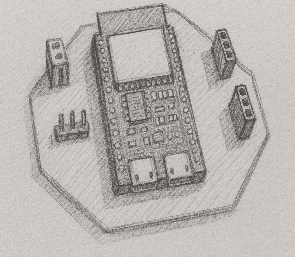
This sketch shows the proposed layout and headers for the PCB, organized to accommodate different types of sensors and peripherals during testing.
4). Software Setup
For this assignment, I used Fritzing as my PCB design tool. One of the advantages is that our university provides a fully licensed version, so I didn’t need to go through the full installation process this time.
However, I’ve installed Fritzing before on a personal computer. The process is very simple and user-friendly: just download the installer, select the destination folder, and follow the on-screen steps. Once installed, you only need to enter the licensing credentials (if required) to unlock the full version.
This is the Fritzing logo you'll see when launching the application.
Once inside the program, the interface is clean and organized. The top area contains the toolbar, while the main workspace is split into multiple views:
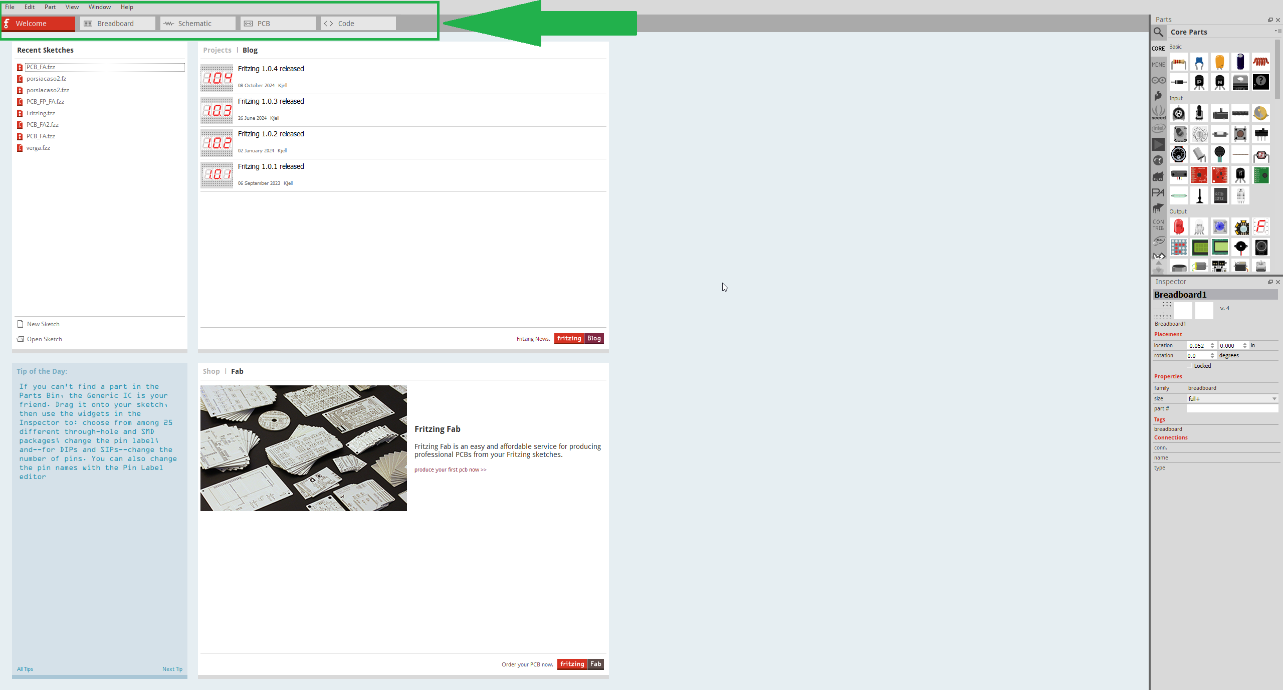
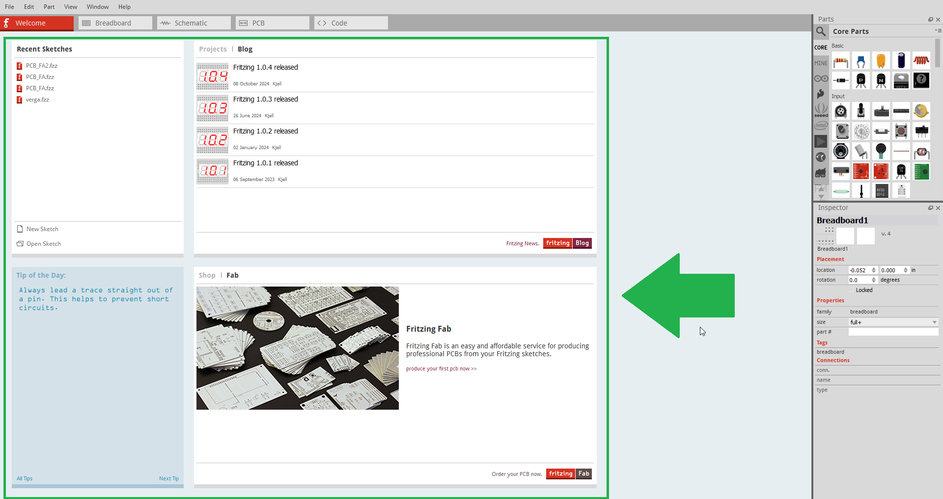
On the right, you’ll find the Parts Library — the most important section of the software. Here you can search for electronic components and drag them directly into your design.
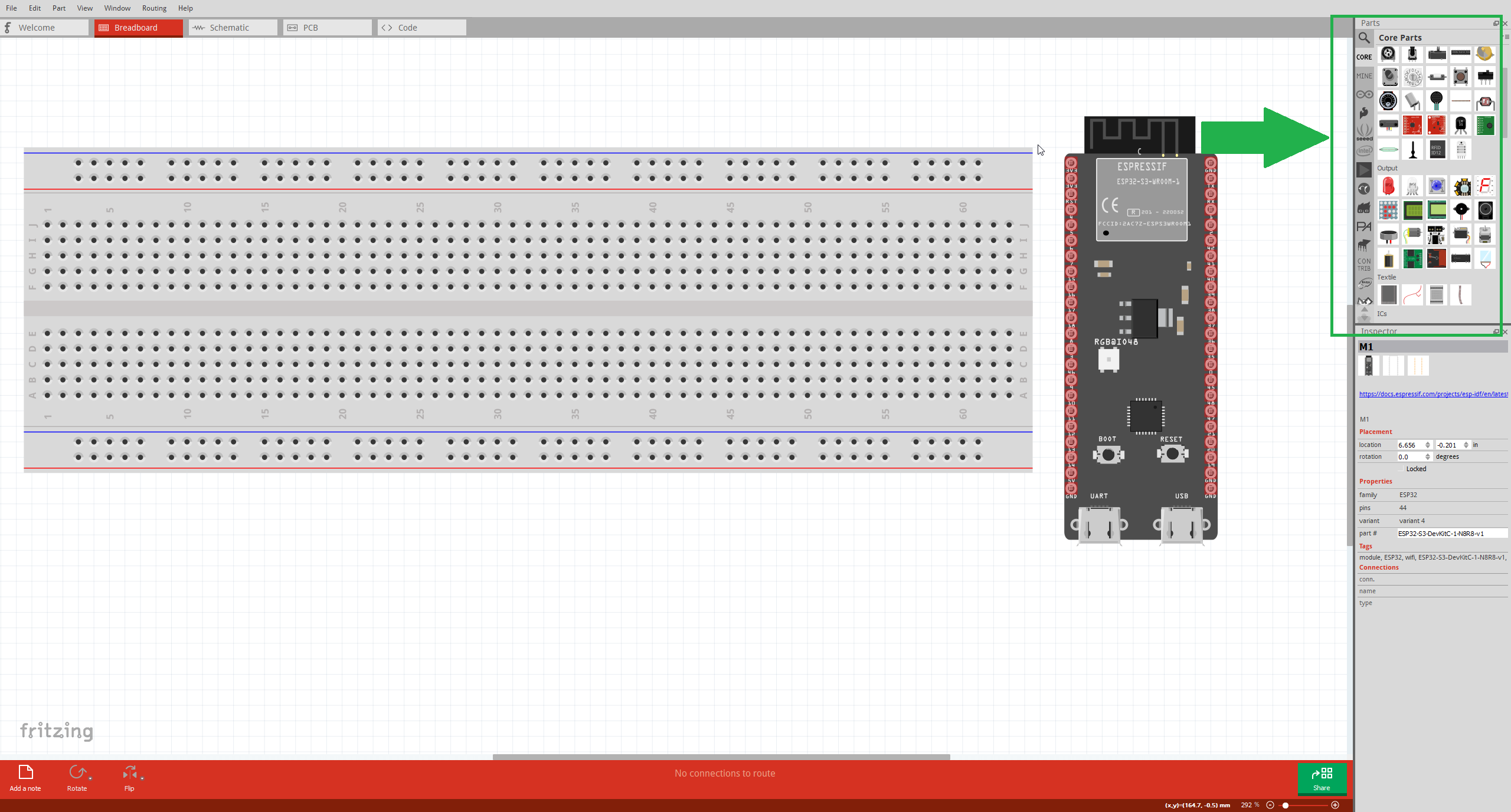
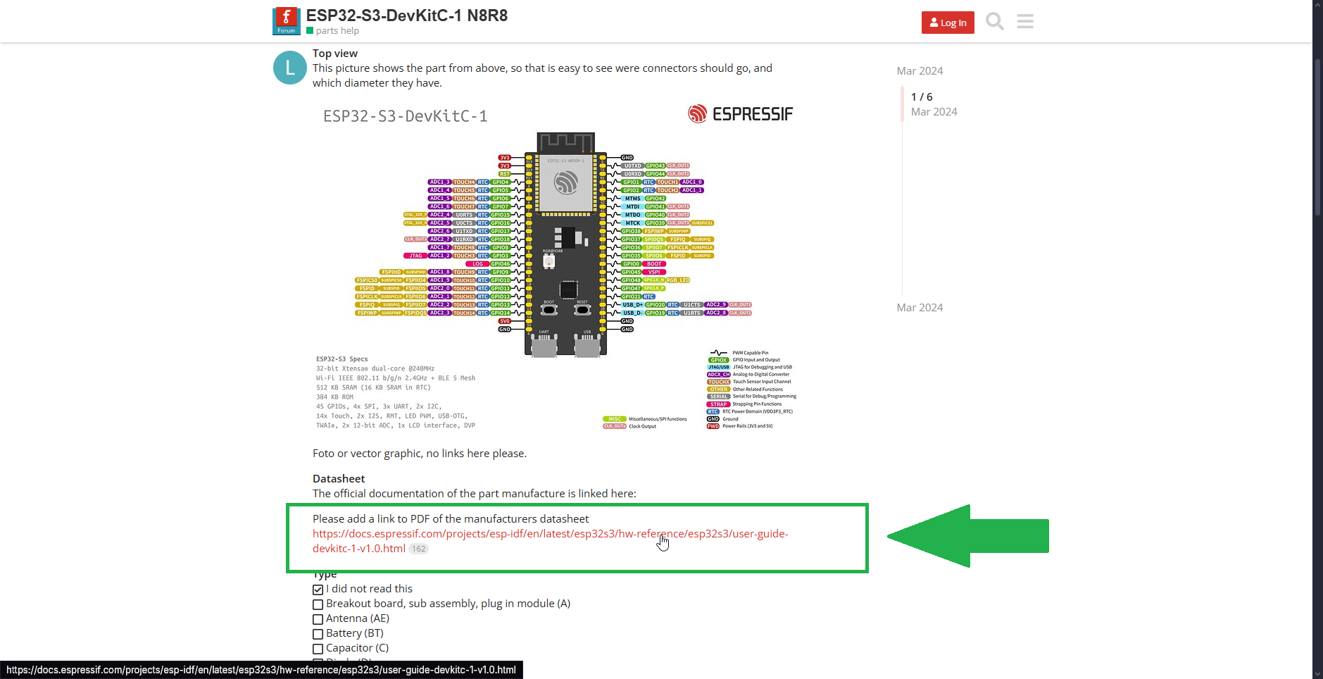
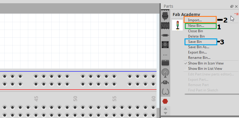
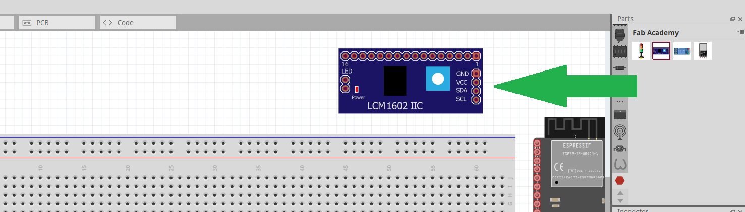
📦 How to Add Custom Parts
If a component is missing from the library, you can easily find custom parts online. Below is a simple example showing how I searched for a part on Google, downloaded it, and added it to a custom bin within Fritzing.
|
Step 1 - Search for part on Google
|
|
Step 2 - Download .fzpz file
|
|
Step 3 - Import into a custom bin
|
|
Step 4 - Use it in your design
|
5). Circuit Assembly (Protoboard View)
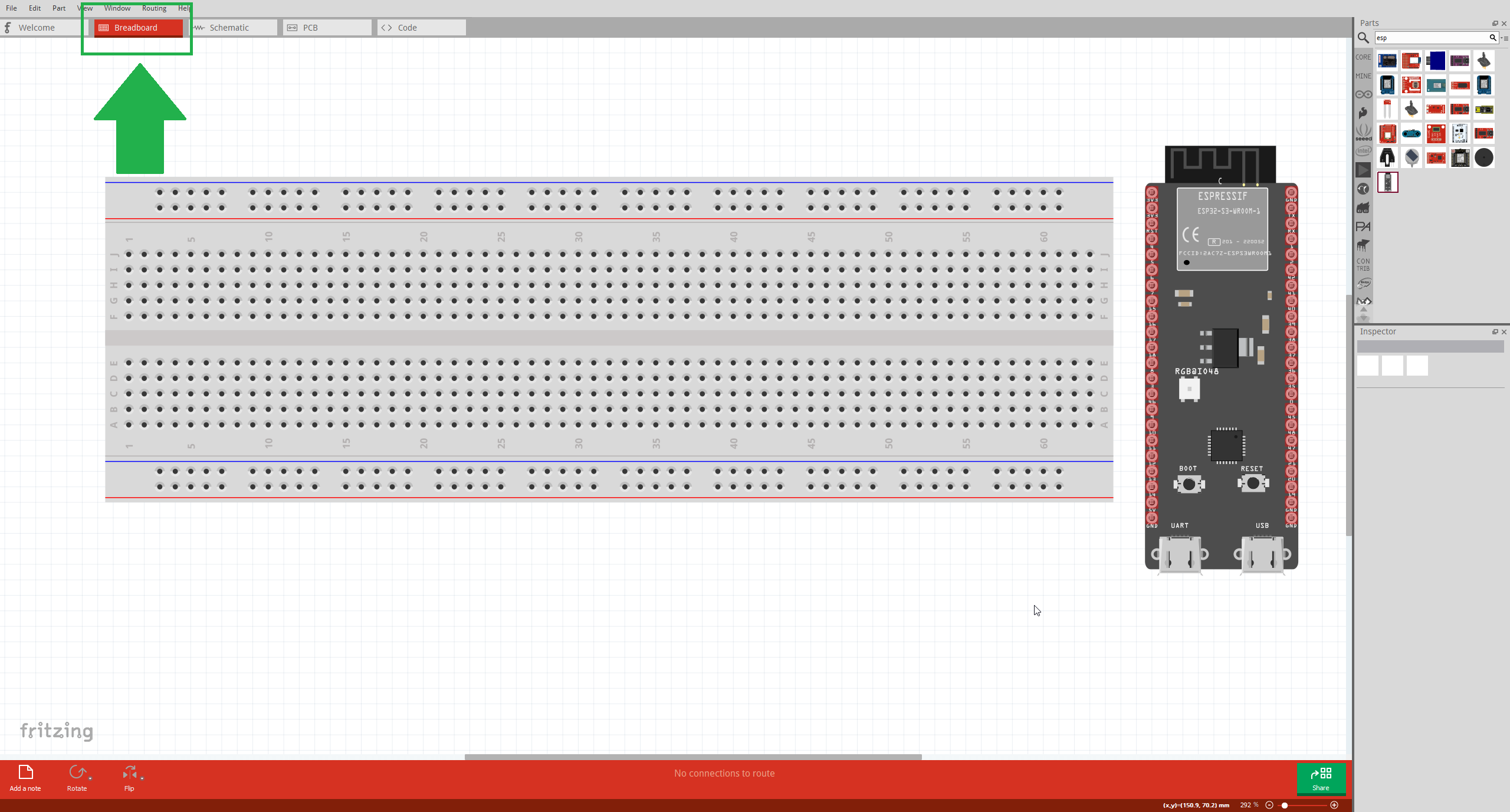
Not all components I needed were available by default in the Fritzing library. For this reason, I searched online and added them as a custom bin. One of the most important parts was the ESP32-S3, since it is the core of my board. Even though I plan to connect it using headers, I needed an accurate footprint to visualize pin positions, spacing, and logical connections.
I used the protoboard view in Fritzing to start the circuit layout. Here I placed the components and manually made all the connections based on the expansion design I planned earlier. Since I am designing a single-layer PCB, I made sure to arrange the wires and parts in a logical way, avoiding overlaps and crossing lines.
The intuitive interface of Fritzing allowed me to drag, align, and connect elements easily. I also used color-coded wires and added custom labels to identify connections clearly. These visual aids helped me organize the layout and will guide me when transitioning to the schematic and PCB views.
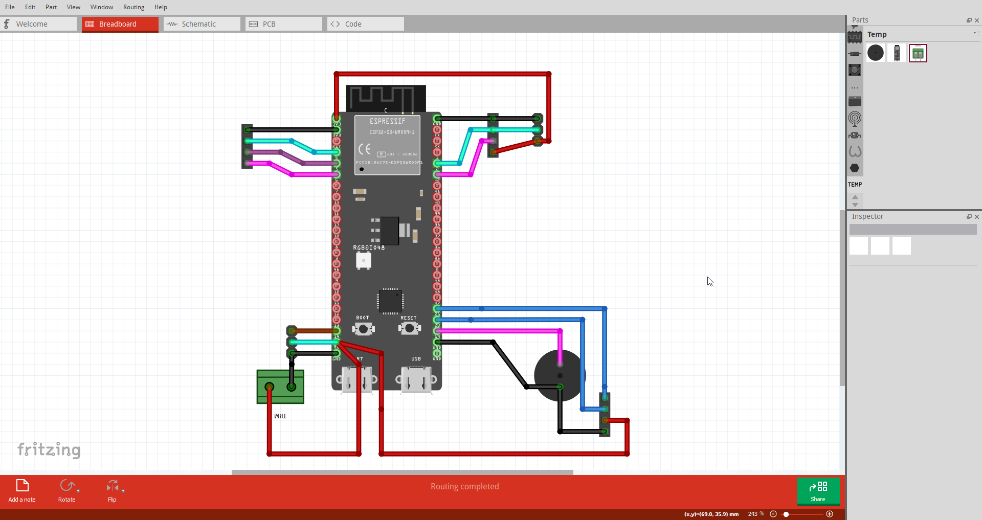
This image shows the protoboard layout created in Fritzing. The ESP32-S3 module was added as a custom part to ensure accurate spacing and logical routing for future PCB fabrication.
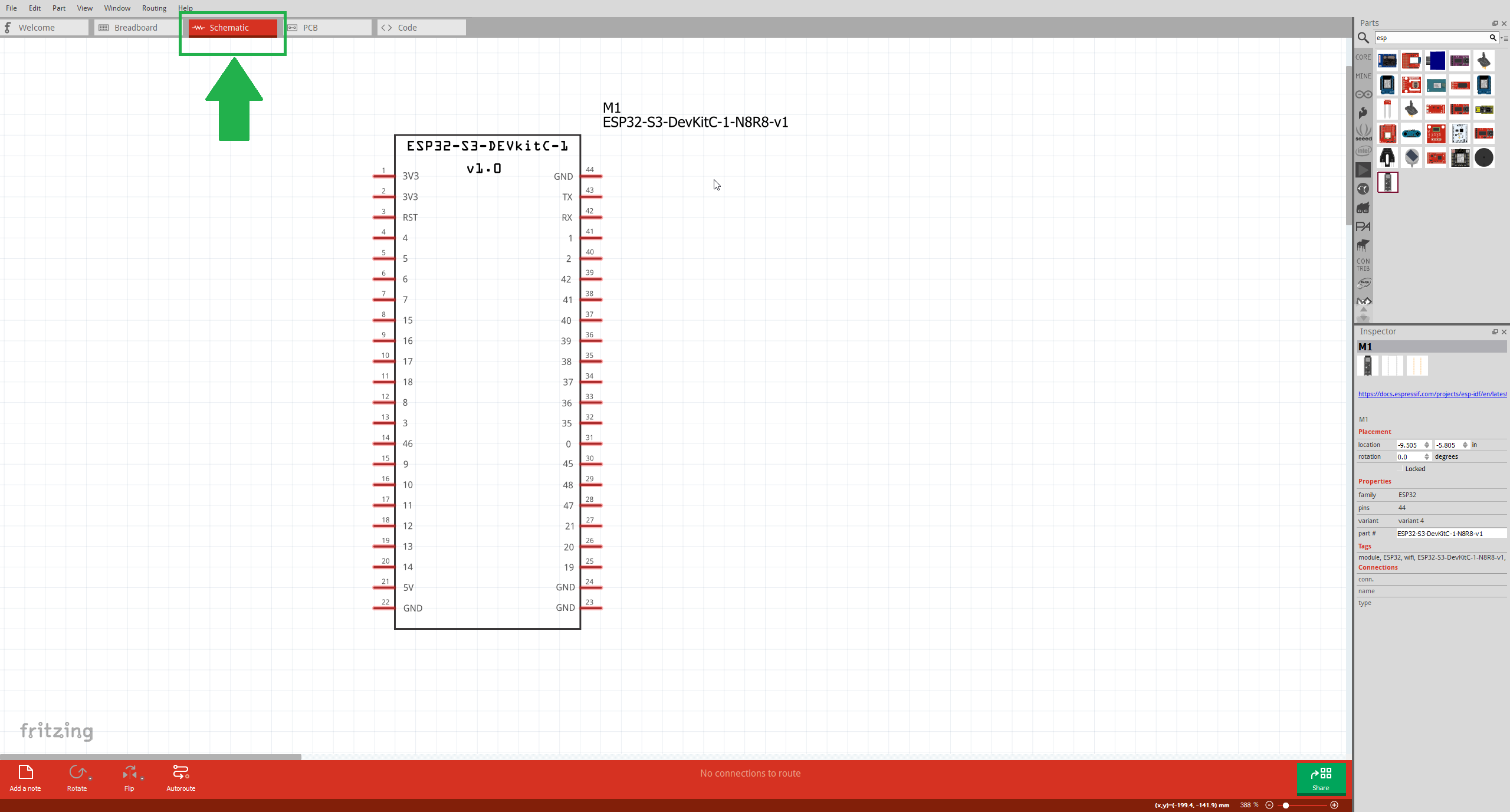
6). Schematic View Design
After completing the protoboard view, I moved to the schematic view to organize the logical connections of my circuit. This part was a bit more challenging, since I’m still learning how to read and design schematics properly.
My main goal at this stage was to keep the wiring clean and structured, avoiding overlapping connections and ensuring that each component was correctly represented. I didn’t go deep into electrical conventions yet, as I know I need to study more about proper schematic design, but I tried to keep it as close as possible to the PCB layout I envisioned.
The schematic is essential because it defines how components are logically connected, regardless of their physical position on the board. It helps detect errors early in the design process, ensures signal flow is correct, and serves as a reference when laying out the PCB. Tools like Fritzing allow you to switch between schematic and layout views, making it easier to spot mistakes and keep both representations aligned.
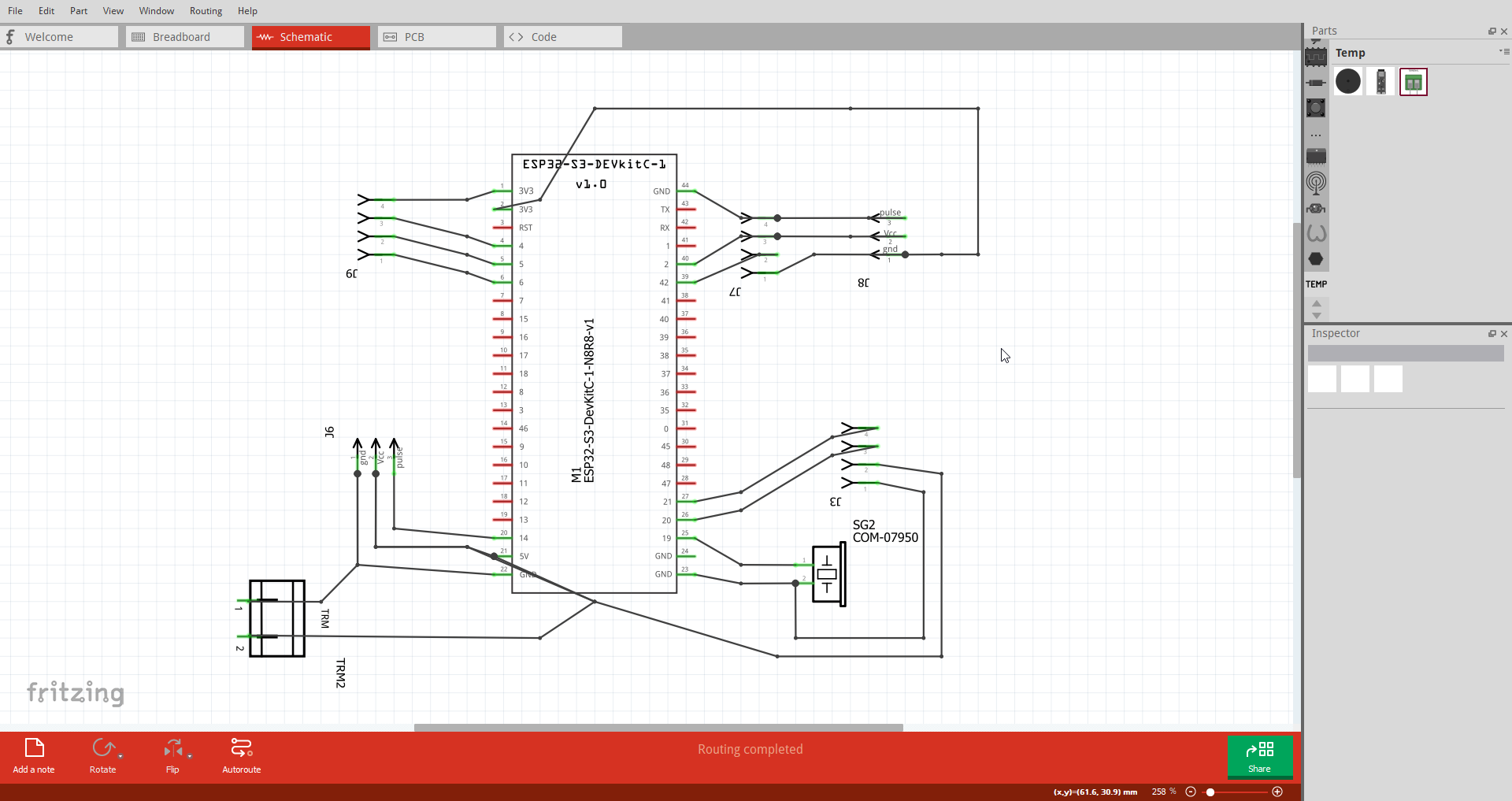
This is the schematic view I created in Fritzing. While I still rely heavily on the protoboard layout for now, this representation helped me verify all connections and plan the next step: the PCB design.
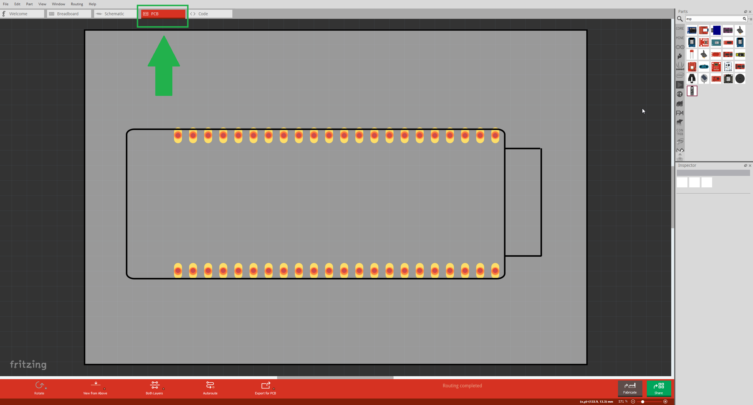
7). PCB Layout Design
For this part, I wanted my PCB to have a specific geometric shape. Since Fritzing doesn’t offer advanced shape editing, I designed a custom hexagonal outline using Inkscape. I’ll go deeper into how to create the custom vector in the next section, but for now, I imported it as a custom shape and started positioning components inside it.
My copper-clad PCB has a maximum usable area of 10 cm x 10 cm, so I had to fit everything within that size. Since a hexagon is not rectangular, I lose usable space in the corners — this forced me to organize the layout efficiently.
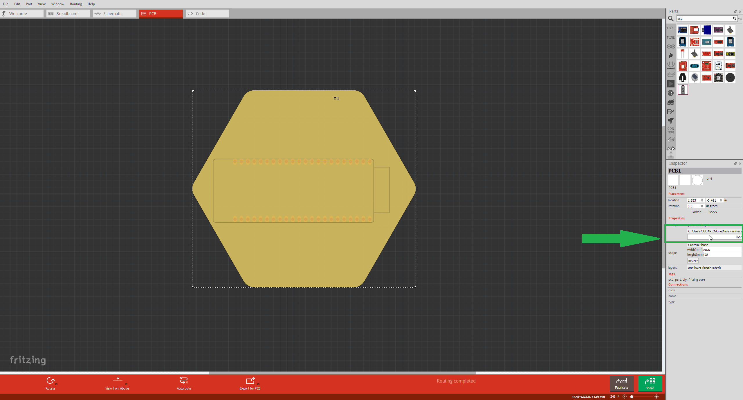
This is my PCB layout inside the hexagonal outline. The shape was designed in Inkscape and imported into Fritzing.
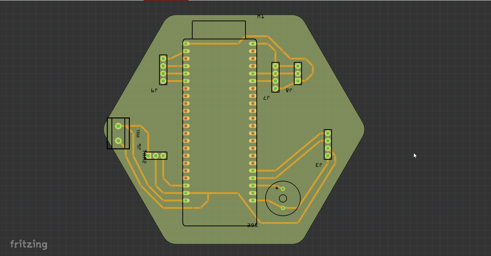
Fritzing offers an autorouting feature, but I found it not very reliable for my layout. It produced inefficient paths and occasionally ignored optimal connections. Because of that, I ended up manually rerouting several traces to make the design cleaner and more functional.
Once all the traces were placed, I double-checked for overlaps and alignment. This manual process gave me more control and made sure my final board met all basic standards for manufacturing.
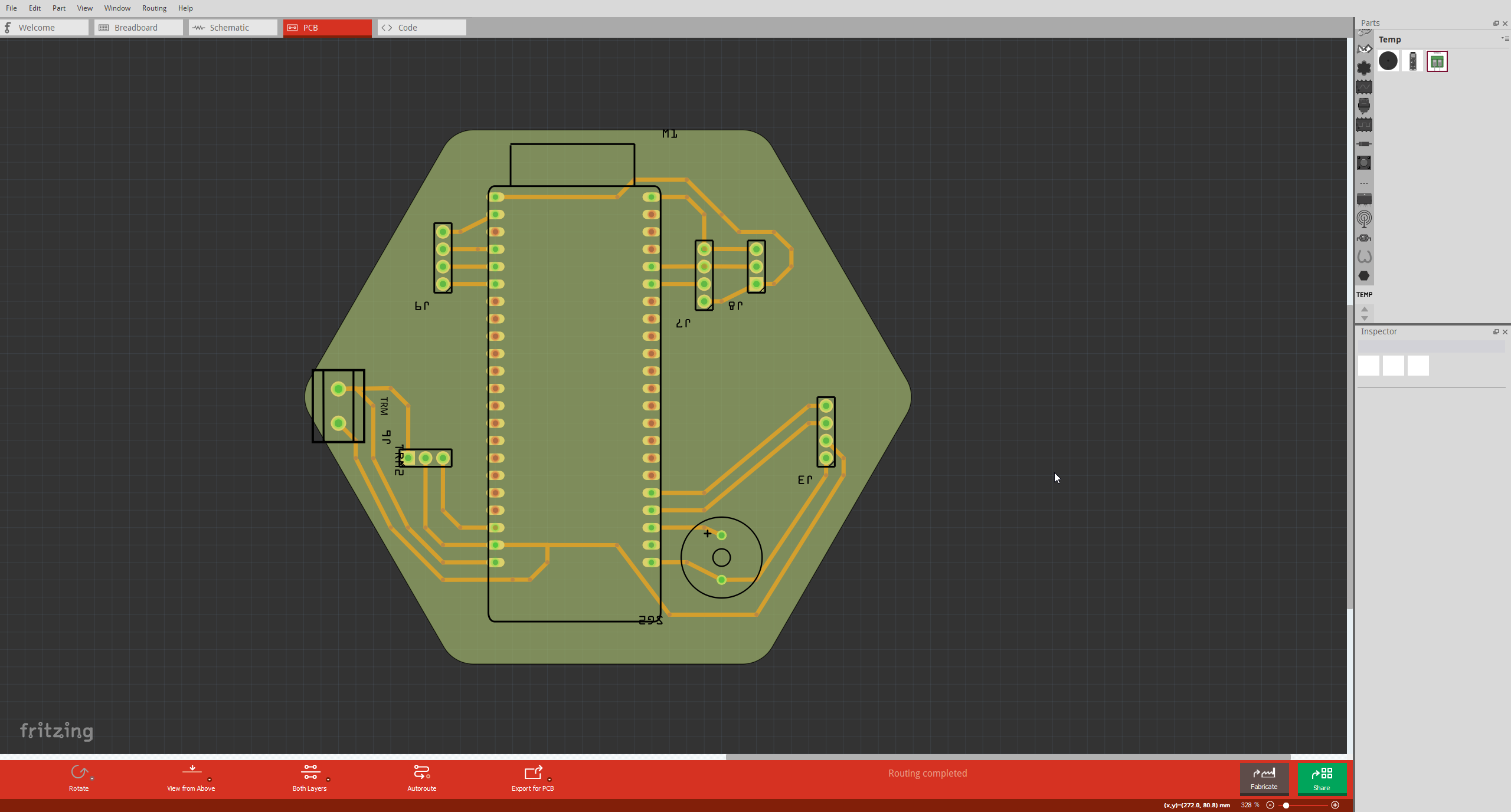
Final routed PCB in Fritzing. Some traces were manually adjusted after disabling the autorouter.
7.1 Custom Contour & Track Widths
Fritzing's default board outlines are rectangular or circular — both adjustable, but limited in customization. For a more personalized PCB shape, like a hexagon, you need to import a custom SVG created in a vector editor such as Inkscape.
I designed my hexagon in Inkscape with rounded corners and a final size of 10 cm across. Then I followed the specific format and structure required for Fritzing to interpret it correctly.
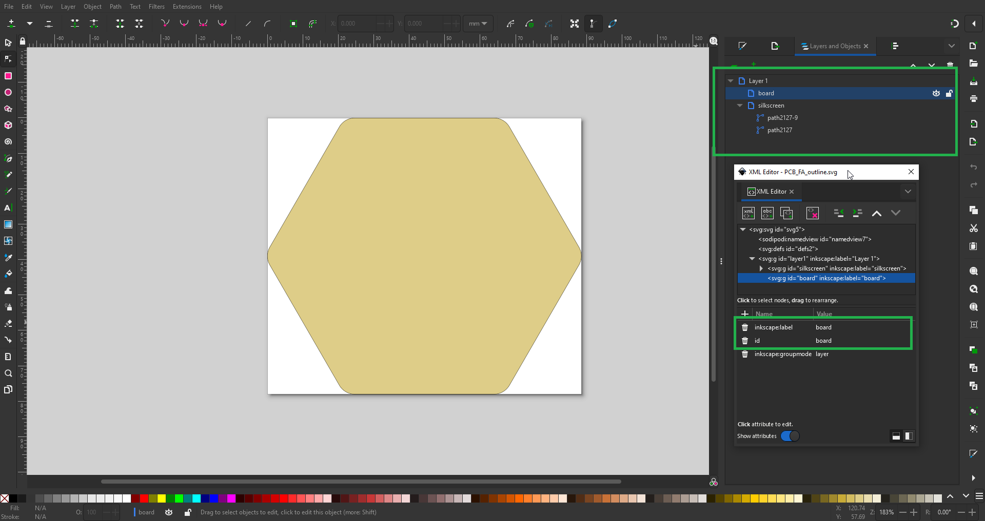
Screenshot showing the SVG structure and naming conventions used in Inkscape to define a valid board outline for Fritzing.
Requirements to create a custom PCB shape in Fritzing:
- The file must be in
.svgformat. - The board outline must be in a layer or group named
board. - The outline must be a closed vector path (no open lines).
- All dimensions must be in millimeters (or scaled accordingly).
- Use no fills and set a stroke width of 0.1 mm (or ~0.27px) for outline visibility.
- The final file should only contain the outline, no extra objects or layers.
I followed the steps from the following video tutorial which explains the full process: https://www.youtube.com/watch?v=ydcOzbCJltg
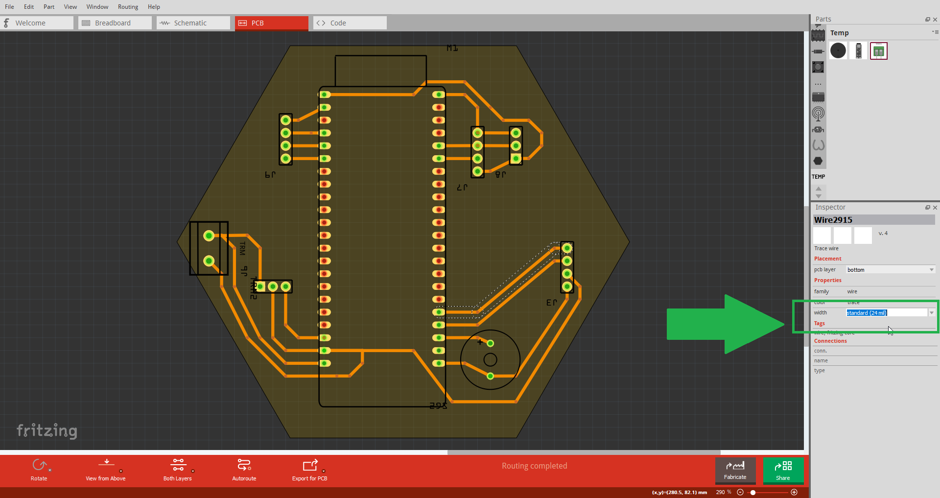
In Fritzing, you can manually change the width of each trace. This is done by selecting a track and adjusting the width from the right-hand menu.
8). Final Review and DRC
While working on my PCB, I encountered some doubts regarding electrical validation and layout quality. To guide myself, I asked for support using ChatGPT Plus, which helped me understand the importance of Design Rule Check (DRC).
Since I’m still learning about PCB design rules, I requested a simple checklist to help me ensure that the circuit was safe and ready for fabrication. The result was a set of easy-to-follow steps:
- 1. Everything is connected
- 2. Tracks are not too close together
- 3. Track width is appropriate
- 4. No components are outside the board area
- 5. 🧠 Run the DRC tool
I went through each item carefully, reviewing the layout and making sure nothing was overlooked. These small checks helped me catch some minor issues early. Once everything was in place, I ran Fritzing’s DRC tool for a final validation.
This step is critical to avoid problems during fabrication, especially since this board will eventually be made using the Makera Carvera, a precision CNC machine available in our lab.
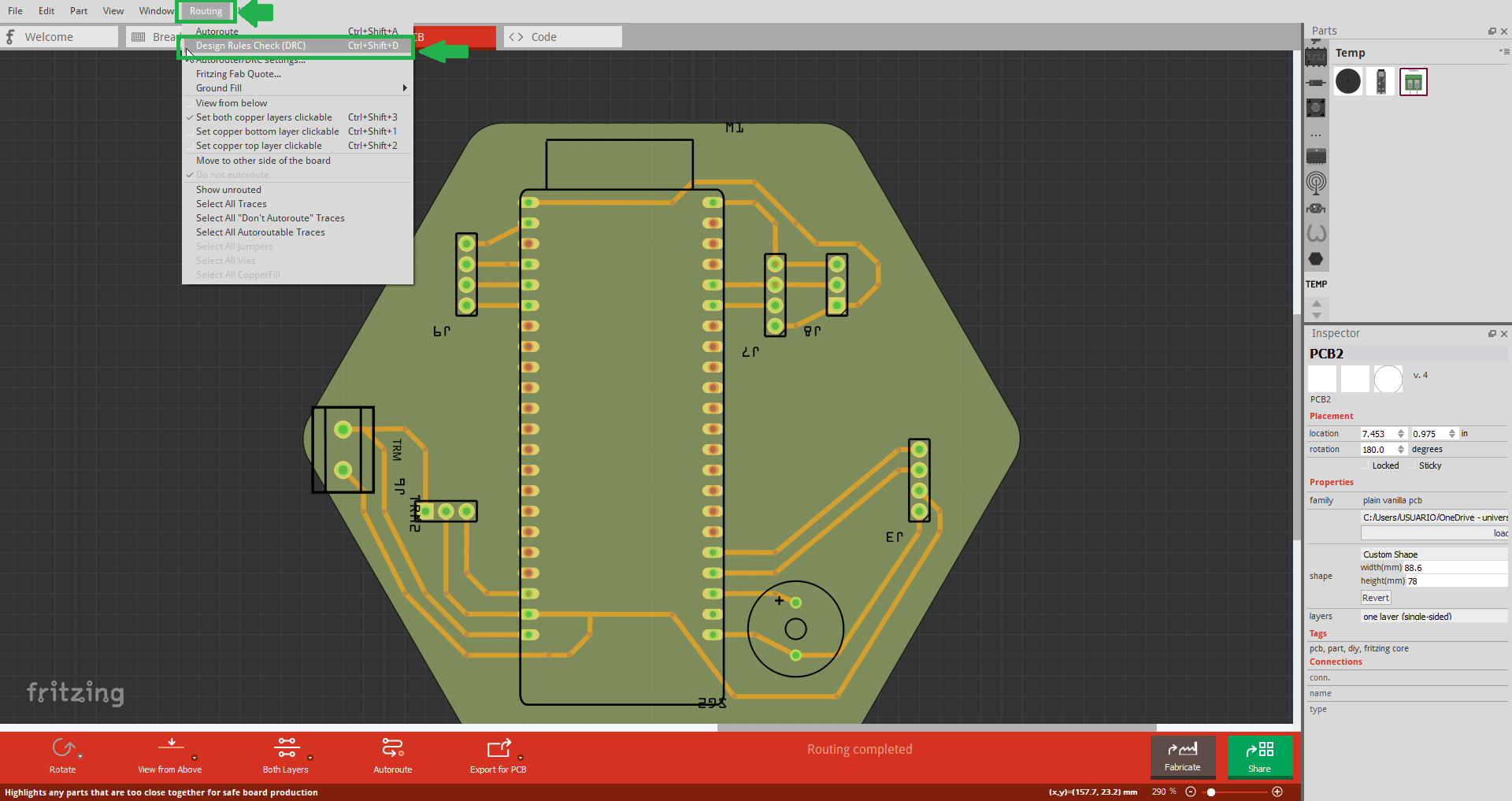
Screenshot of the DRC check running in Fritzing. This tool helped me confirm that no errors were present before exporting.
9). Exporting the Design
The final step is to export the design files. Although I won’t fabricate the board just yet — because I want to study the CNC process a bit more — I’ve prepared the files for future use.
This PCB will be manufactured using the Makera Carvera, a high-precision CNC machine controlled via Fusion 360. For this reason, the best formats to export are SVG or DXF, both of which are compatible with CAM tools in Fusion.
I’ve already generated these formats directly from Fritzing and saved them in my project folder, ready for future fabrication.
Conclusions
Personal Reflections and Lessons Learned
Despite having little prior experience with PCB design, this week turned out to be one of the most rewarding so far. I knew that the process could be tricky, so I made an effort to read documentation, watch tutorials, and explore the software thoroughly before starting. That preparation paid off — I didn’t encounter major errors, and the design process flowed smoothly.
One of the key takeaways was understanding how important it is to organize connections from the beginning. Thinking ahead about the board’s shape, logical pin layout, and space constraints helped me avoid messy routing later.
I also appreciated the value of switching between protoboard, schematic, and PCB views in Fritzing. This helped me visualize the design from different perspectives and catch mistakes early.
While I still have much to learn — especially about schematic standards and multi-layer routing — this week gave me the confidence to take on future PCB projects with a more structured and analytical approach.