
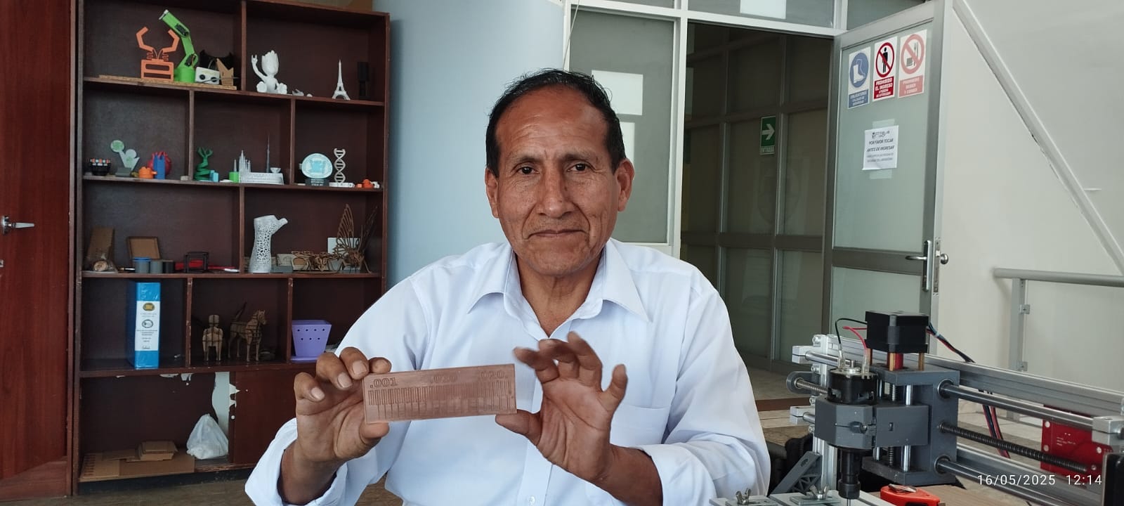
For this group assignment, I will be using the available CNC Router, as our milling machine is out of service. With the help of my instructor Cristian, we conducted several tests and obtained different results.
To start documenting this assignment, I met with my instructor Cristian, who provided some guidance. He shared recommendations based on the work he and his group did last year. The only difference is that, in my case, we don't have a milling machine to make our PCB, but we do have a CNC Router that will also help us with this task.
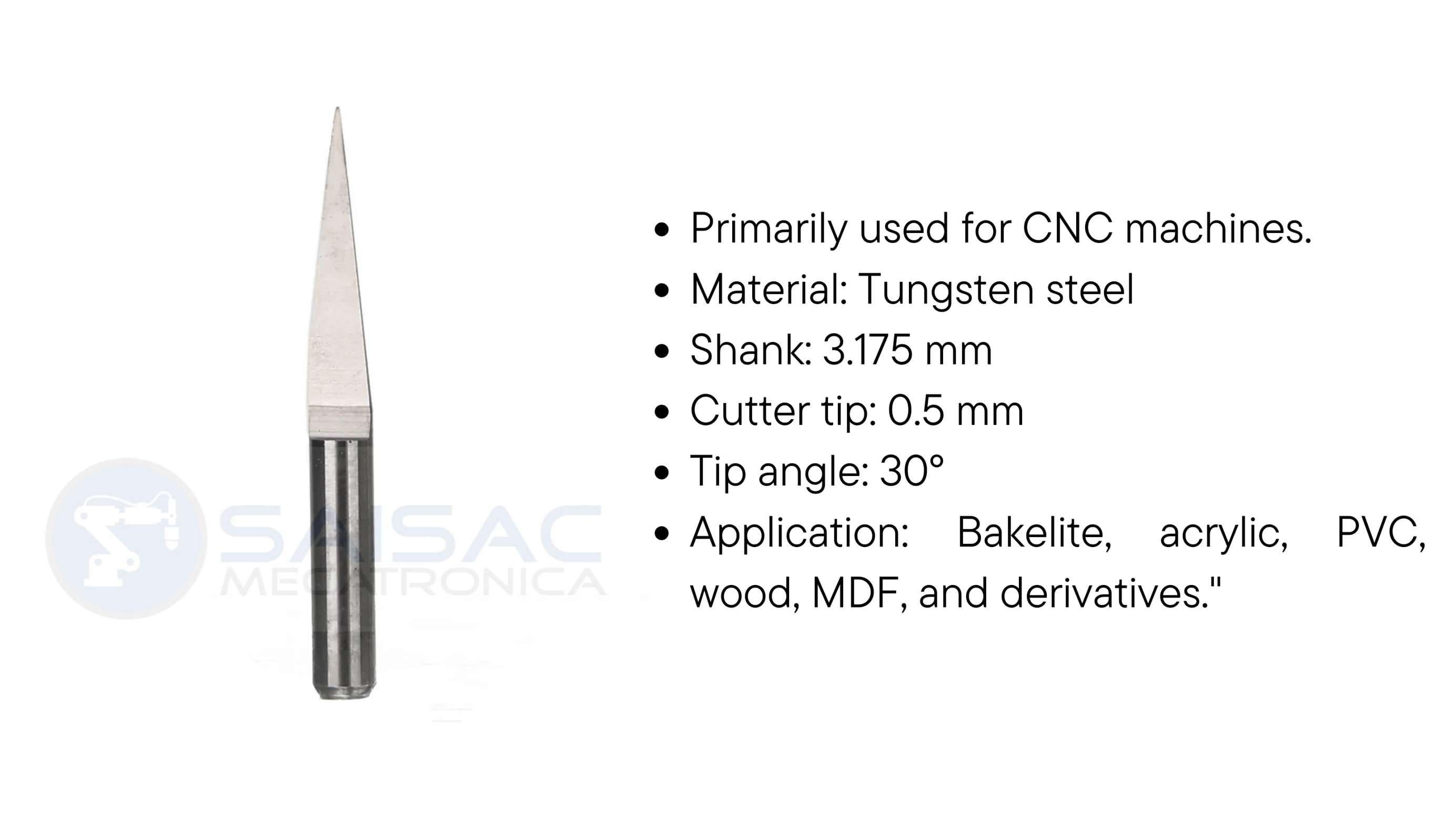
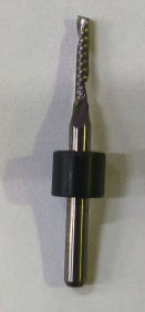
One of the things we were missing in the Fab Lab iFurniture were the end mills. We ended up purchasing a 30° angled end mill and a 0.5mm cutter tip. I found this end mill at the following link. Mecatrónica Saisac
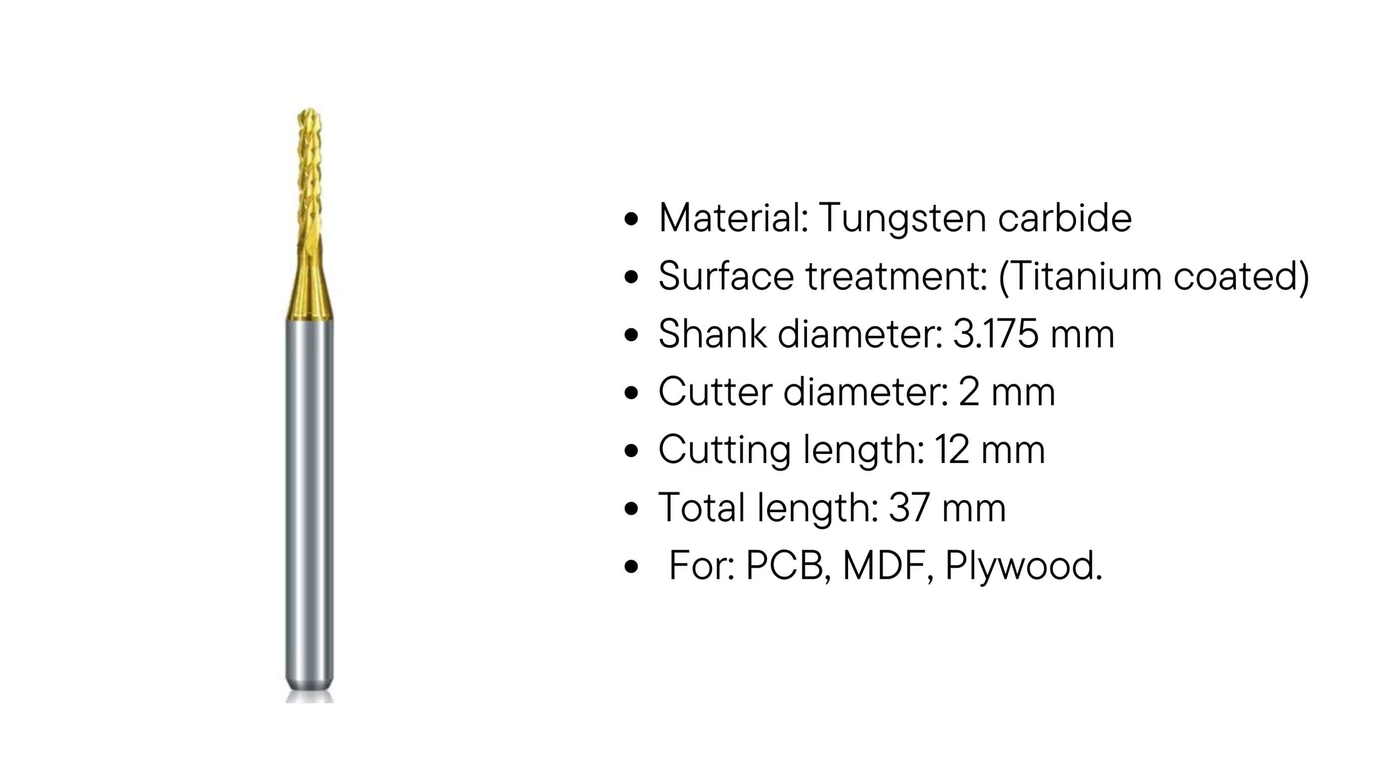
To cut the bakelite material, we purchased another end mill that would assist with the cutting, a cutter with a 2mm diameter. I also found this end mill at the same previous link. Mecatrónica Saisac
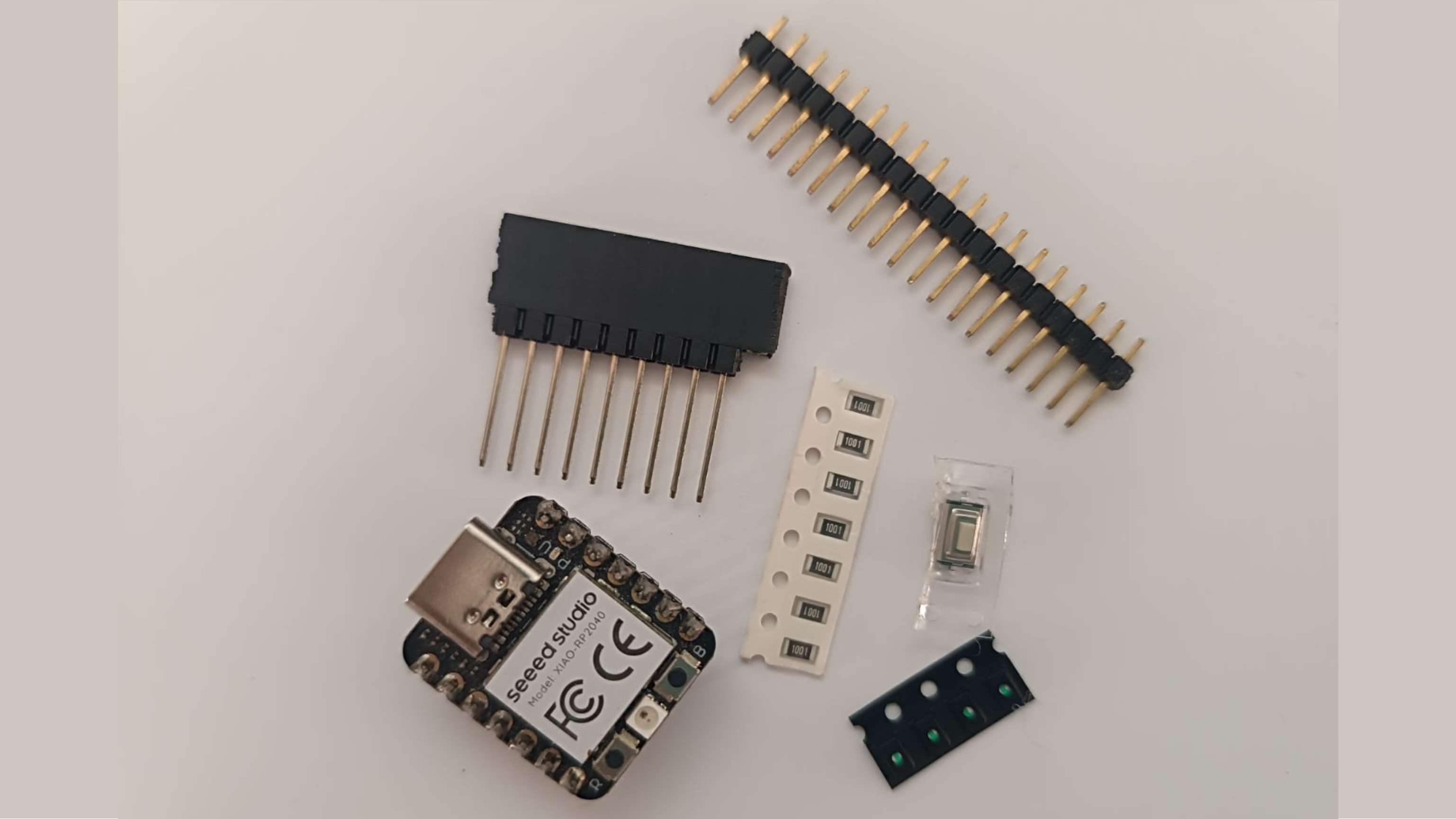
These are the electronic components that will be used in the individual assignment, but it is important to know them for this group assignment. This will help ensure that, when making the cut, we are working at the correct scale.
The machine we will use, which is available and easily accessible, is the CNC Router, the same one we used in the previous assignment. Although it is a larger-scale milling machine, it can also help us carry out this assignment of milling bakelite. This is the first time we are using it in the Fab Lab Ifurniture, so the process will involve trial and learning.
Here are the machine specifications.
| Specification | Details | |
|---|---|---|
| Cutting Area: | 1220 mm x 2440 mm x 150 mm | |
| XY Positioning Speed: | Variable, max. 1800”/min | |
| Z Positioning Speed: | Variable, max. 900”/min | |
| Input Voltage: | Single-phase 220V |
When purchasing the end mills, one of the key considerations was the shank size, which is 3.175 mm, as this is the correct size used by the machine. We decided to replace the previous end mill with a 30° V-shaped end mill with a 3.175 mm shank and a cutting diameter of 0.5 mm.
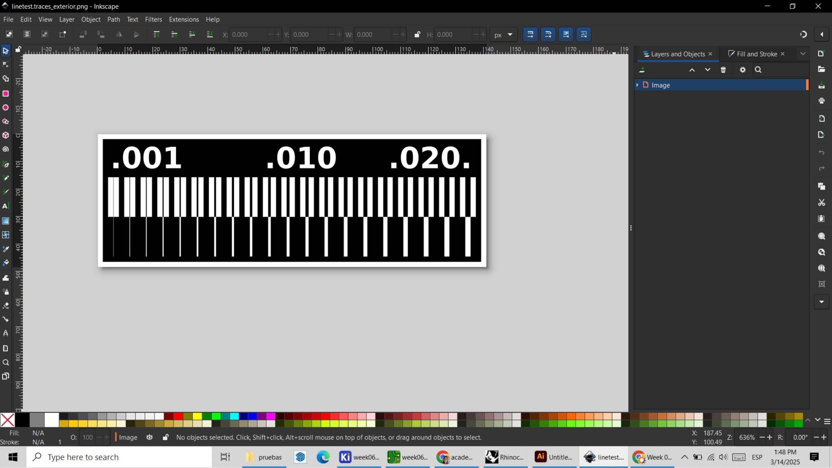
I downloaded the Traces+Exterior file in PNG format from the Academy website. Since the CNC Router we use in the Fab Lab operates with the ArtCAM software and the model configuration needs to be in DXF format, I proceeded to open the PNG file in Inkscape to convert it to the appropriate format.
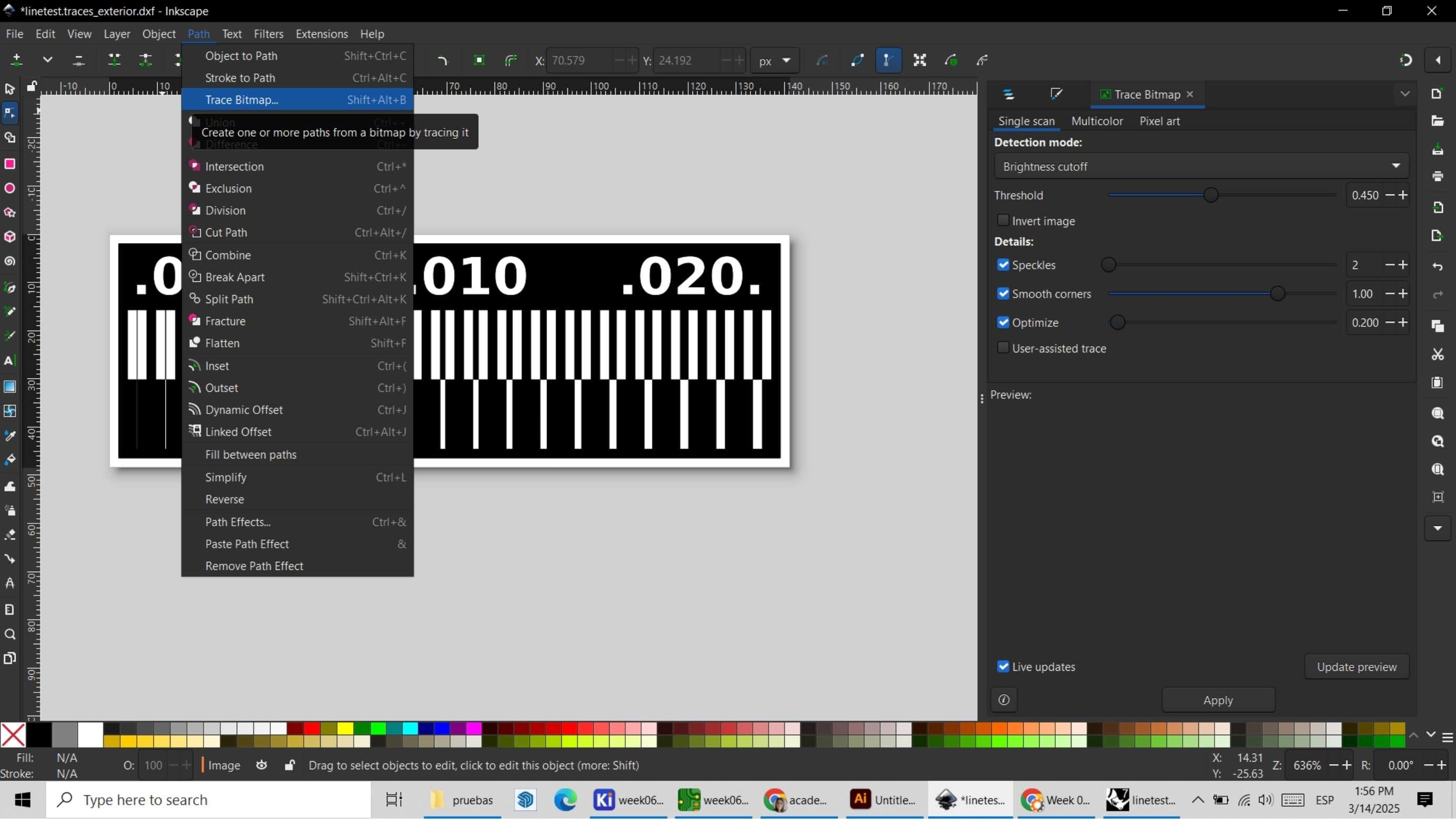
To vectorize this PNG file, I go to the "Path" menu and then click on "Trace Bitmap" to convert the image into a vector file.
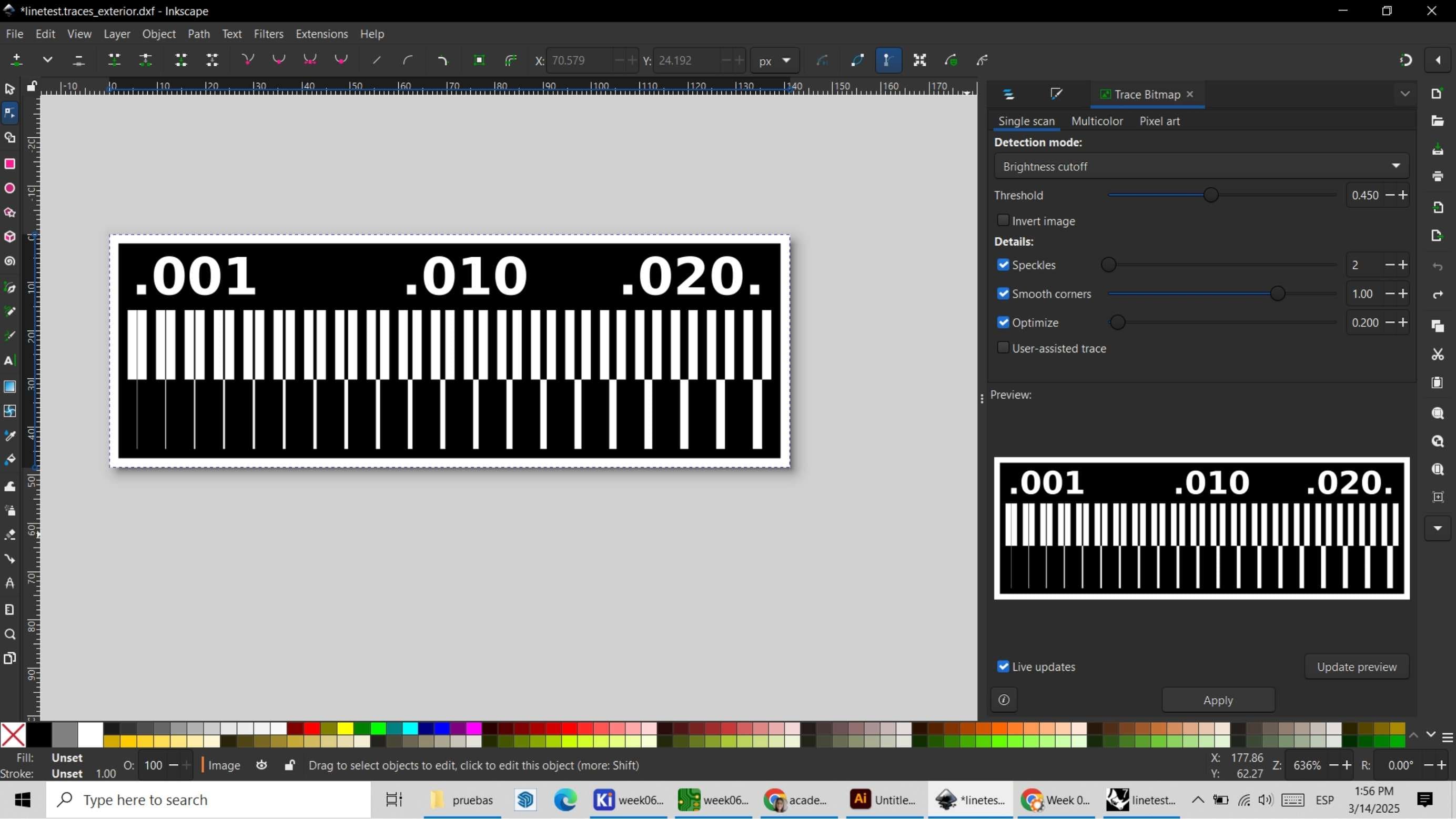
I select the PNG image and press Enter to apply the tracing and convert it into a vector file.
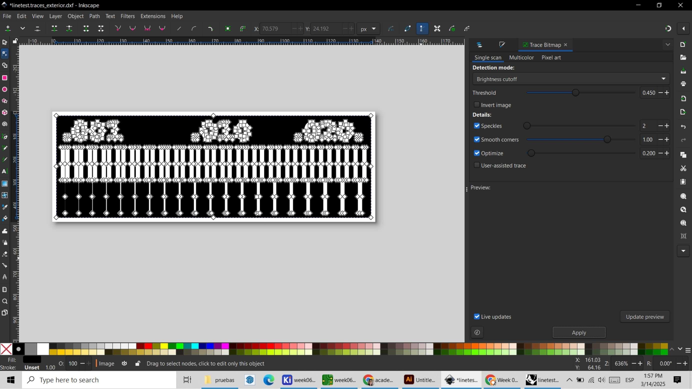
And done! The image is now in vector format!
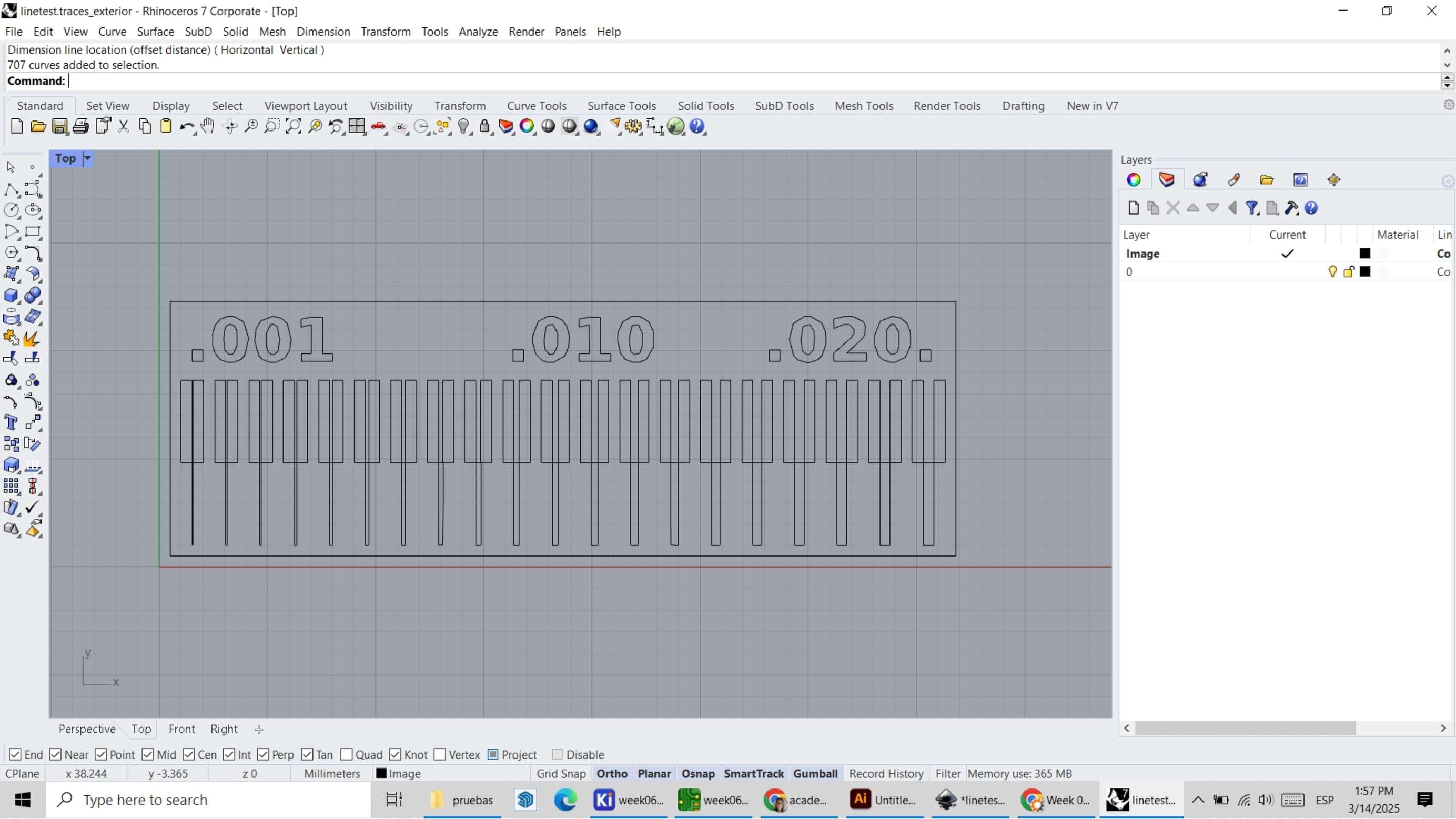
To do this, I open the file in Rhino and adjust the lines to ensure that the ArtCam software recognizes them correctly.
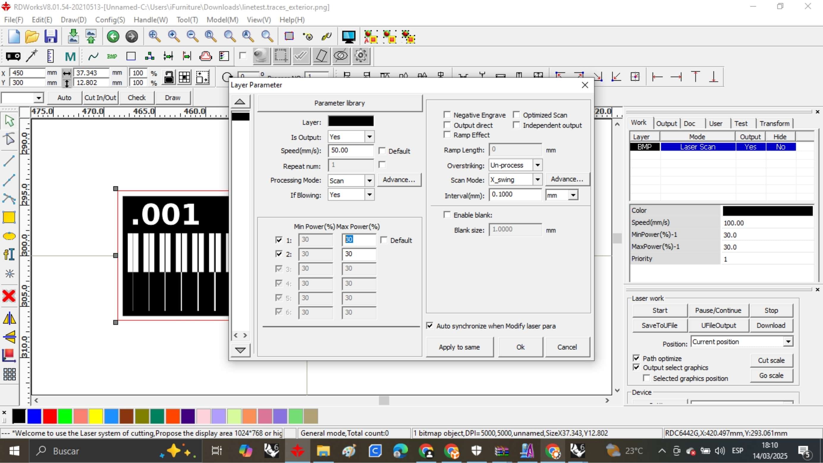
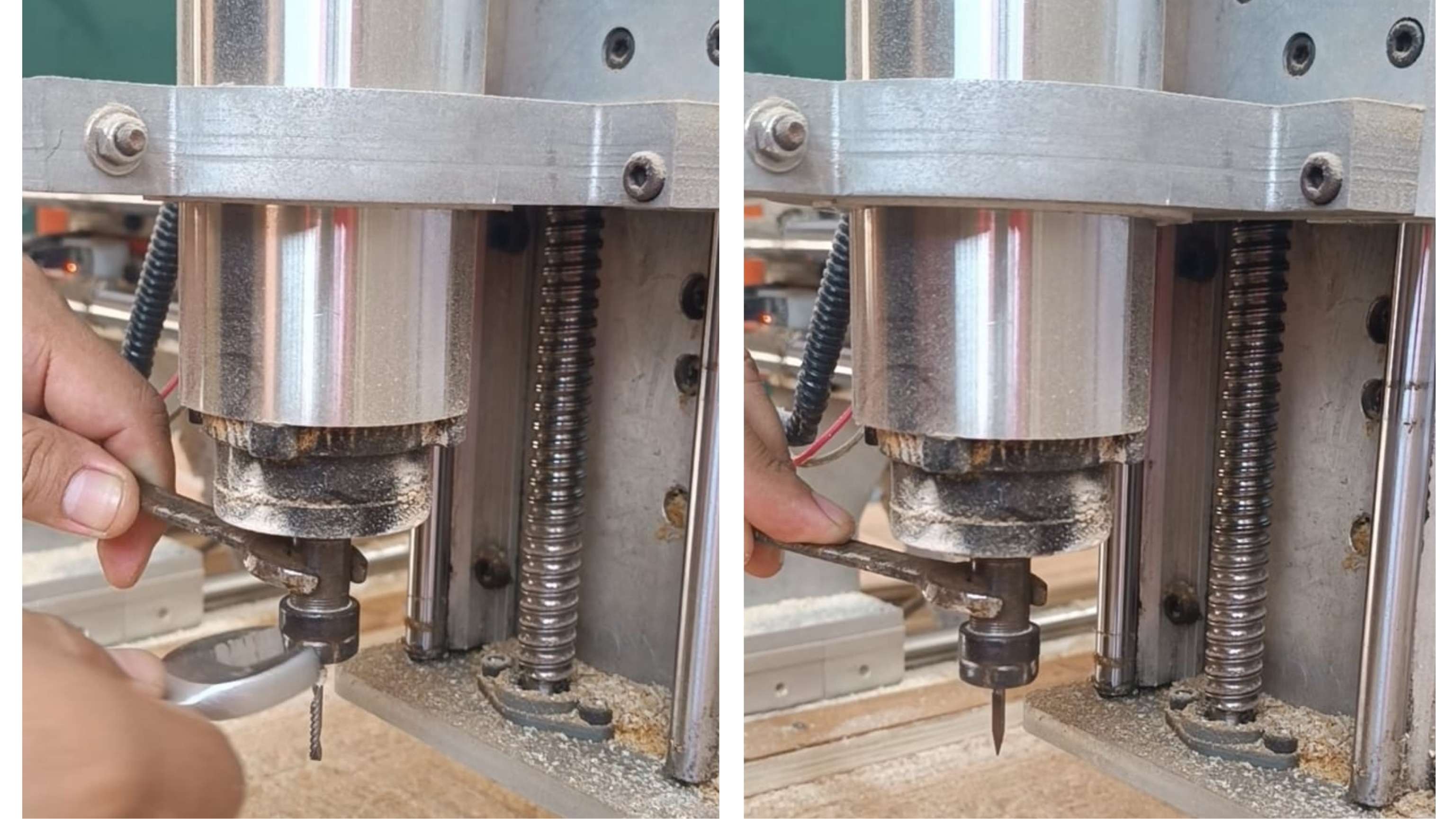
I tried to do this assignment with the laser, but the laser didn't make a dent. So, I took a chance and did it with the Router.
Once the design for the PCB was configured in ARTCAM, I proceeded to cut it with a thin 0.1 mm bit with a 15° angle. We got this bit later to be able to cut my individual project board. The challenge with this board was being able to cut it, but the difference was that the tracks in this design were thinner and the scale was about 37 mm. So, as I was milling the lines, I ended up milling everything. 😞
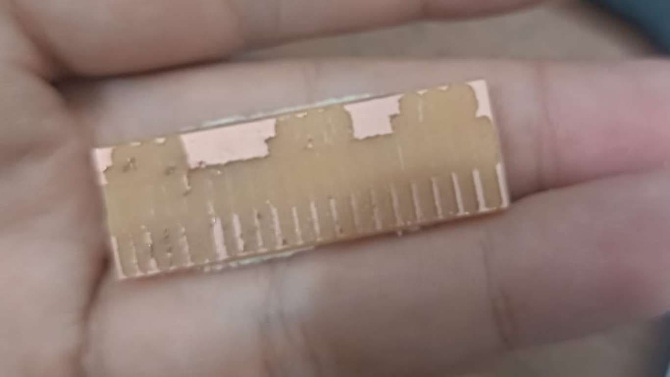
So this little board ended up, sad and empty.

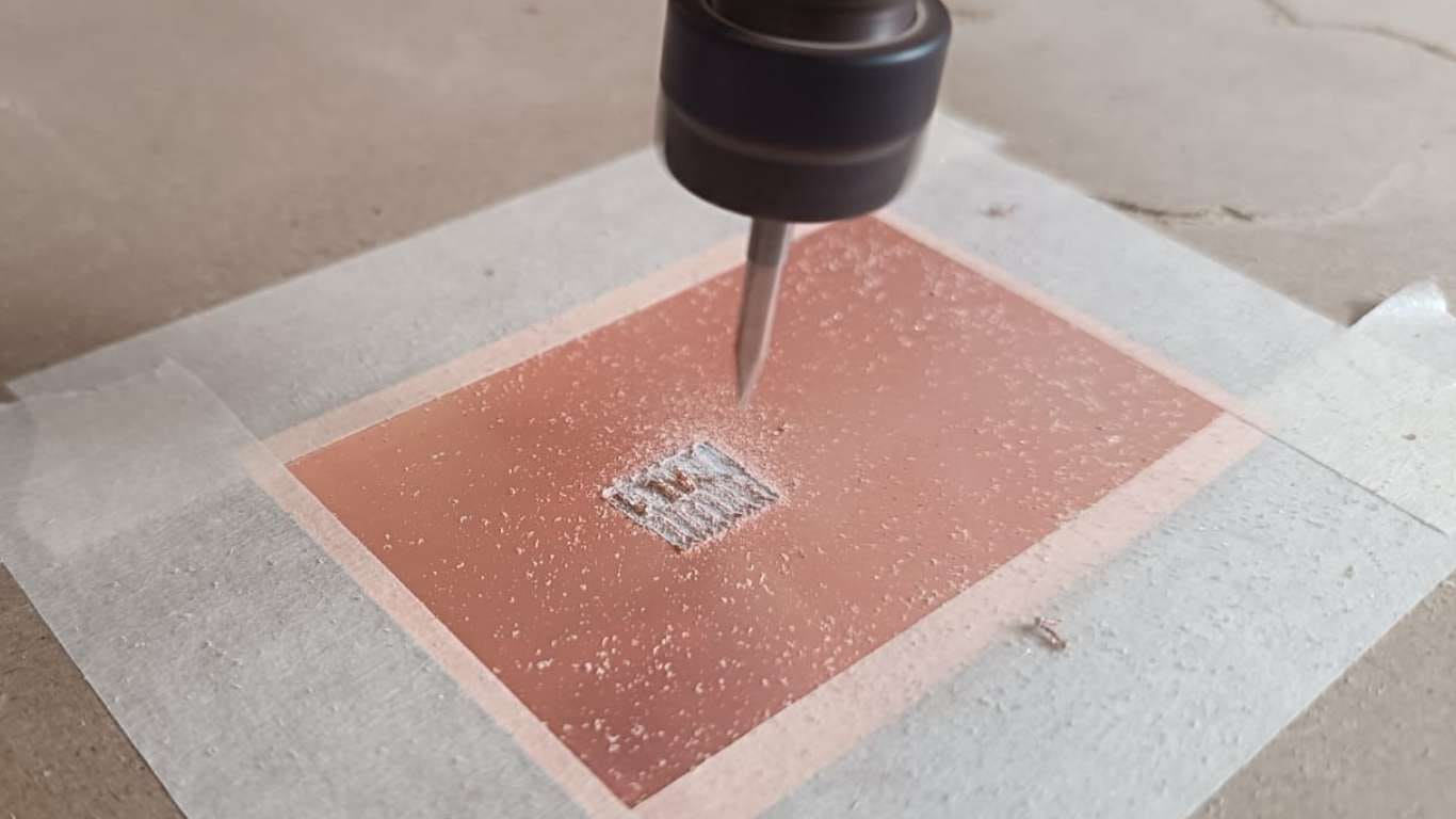
However, since I wanted it to turn out well, in the workshop, they did the cutting service for me so I could see the differences (don't forget to include the specifications).
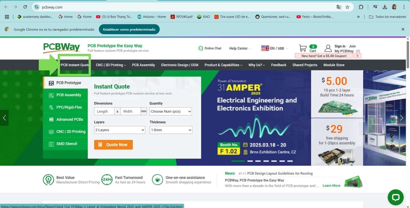
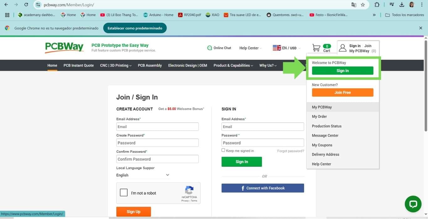
The first thing I do is create an account to access the service on the website.
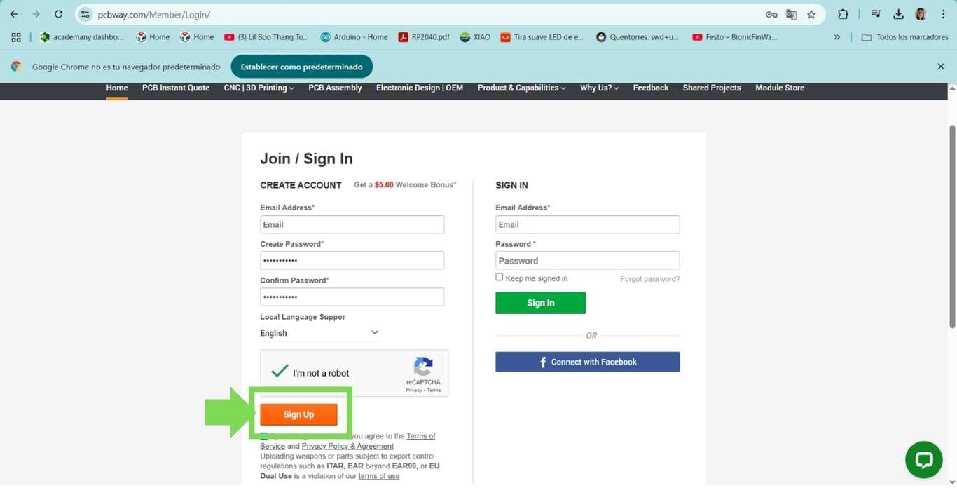
I enter my details, create a password, and that's it, I click on 'Sign Up'.
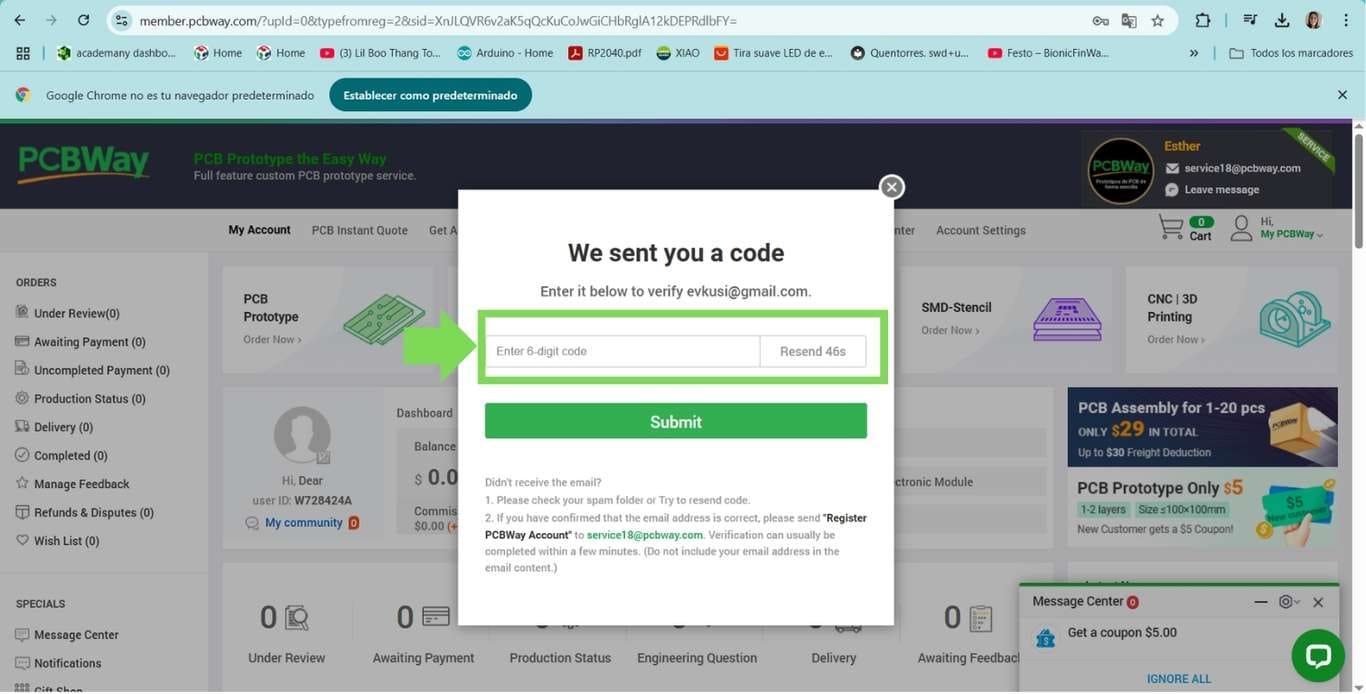
In the box, I need to enter a code that was sent to my email to be logged into the account. Once I enter the code, I click 'Submit'.
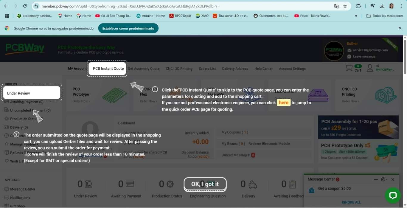
The website gives me a brief explanation of how it works.
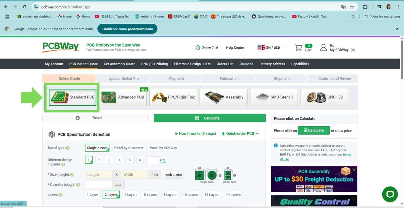
Once this is done, I make a selection of how I want my PCB to be. In my case, I chose 'Standard PCB', which links me to another page.
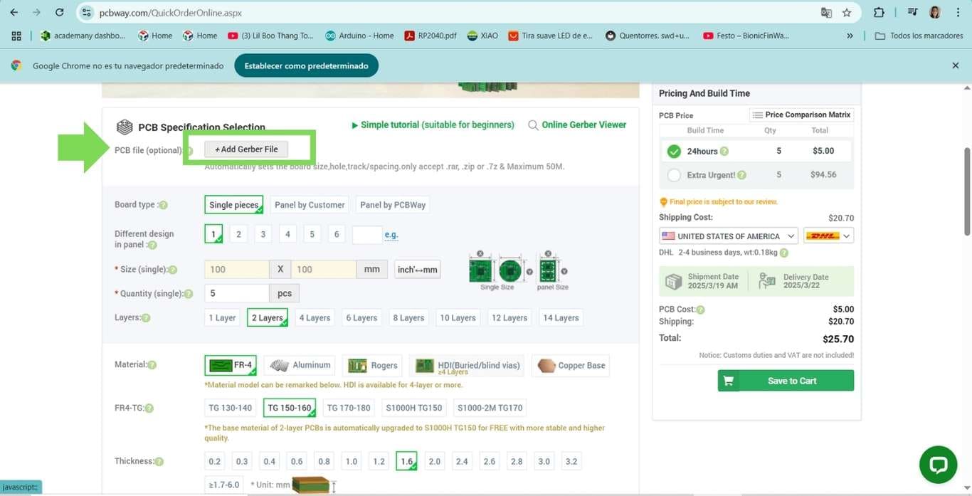
To get a quote for my design, I need to upload the document in Gerber format, which I do from the KiCad software by following the plotting process, and there I find the option to save as Gerber. Once this is done, I upload the design on the PCBWay website.
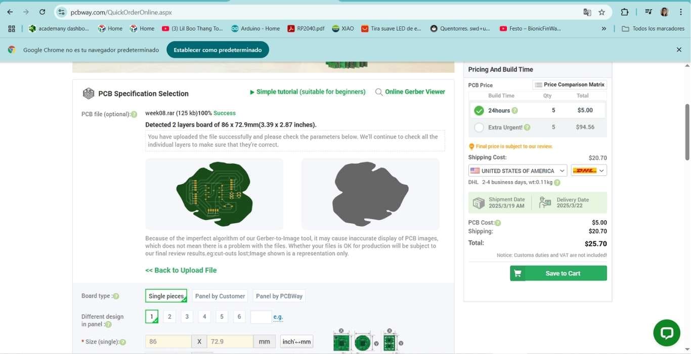
Once that's done, I leave the specifications as default. Now I can see my design previewed on the website.
Now, in the green box area, you can see the price of the PCB and the shipping cost. And you can make the purchase online, just like in any online store.
This week, we used the Makera Carvera, a high-precision desktop CNC milling machine, to fabricate printed circuit boards (PCBs) in-house. Thanks to its automatic tool changer, intelligent surface calibration, and high-speed spindle, we were able to achieve fast, precise, and professional-quality prototyping.

The Makera Carvera is a fully automated CNC machine designed for rapid prototyping and small-batch manufacturing. It supports a wide range of milling operations and materials. Key features include:
We used this machine to mill both the traces and the outline of our PCB using different end mills, ensuring accuracy in every stage of the process.
| Feature | Specification |
|---|---|
| Machine Type | Desktop CNC Milling Machine |
| Work Area (XYZ) | 356 × 234 × 120 mm |
| Spindle Speed | 3,000 – 24,000 RPM (variable via software) |
| Tool Holder | Automatic Tool Changer (ATC) with 4–6 tool slots |
| Supported Tool Diameter | 0.2 mm – 6.0 mm |
| Max Feed Rate | 2000 mm/min |
| Repeatability | ±0.01 mm |
| Z-Probing & Auto-Leveling | Yes – built-in smart surface probing system |
| Camera System | Integrated (for origin detection and alignment) — optional use |
| Supported Materials | FR1, FR4, Acrylic, Wood, Aluminum, Waxes |
| Axes | 3-axis standard + optional 4th rotary axis |
| Connectivity | USB-C, Wi-Fi, SD card |
| Control Software | Makera Carvera App (G-code compatible) |
In our project, we used the 3-axis mode, auto-leveling, and automatic tool changes. The spindle speed was adjusted based on the milling stage, and FR1 board was selected for its machinability.
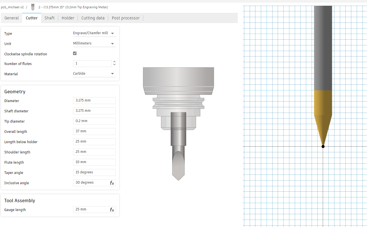
This tool is ideal for trace isolation on copper-clad boards like FR1. Its fine tip allows for sharp path definition while minimizing burrs. It was selected for its precision and compatibility with thin copper layers.
This flat end mill was used to cut the outer contour of the PCB. Its flat tip ensures clean edges on FR1 boards, and its single flute design helps remove material efficiently without overheating. It was selected for its durability and smooth finish.
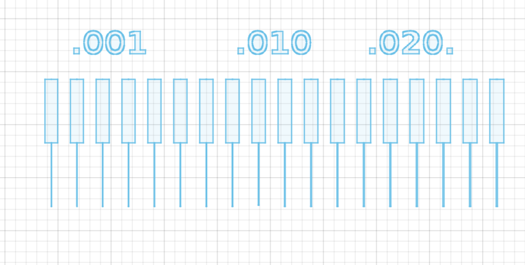
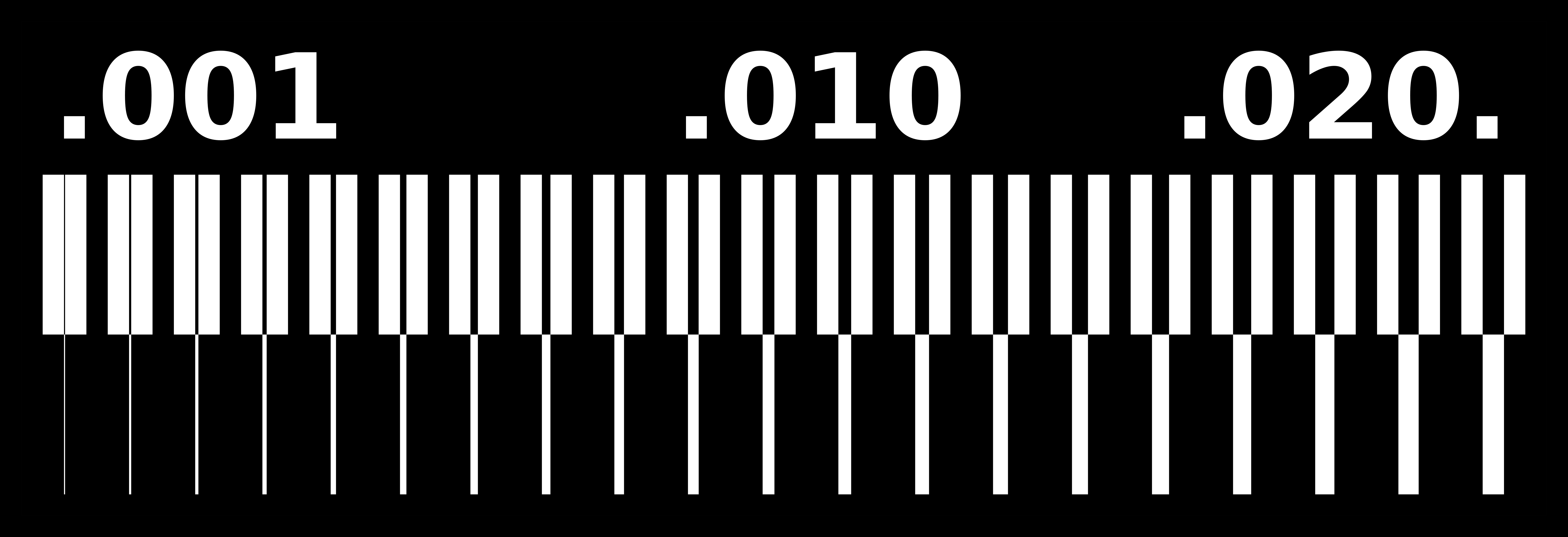
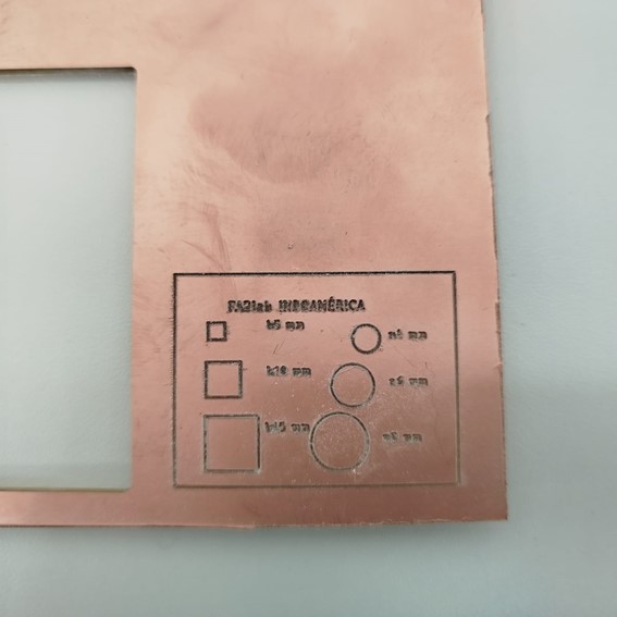
To characterize the engraving resolution and milling accuracy of the Makera Carvera, we created a custom trace isolation test using Fusion 360. The design includes a sequence of lines and gaps labeled 0.01, 0.10, and 0.20 mm, which represent progressively wider spacing between features.
This test allowed us to:
This tracing test pattern was milled before processing the final PCB to ensure tool compatibility and accuracy with the FR1 material.
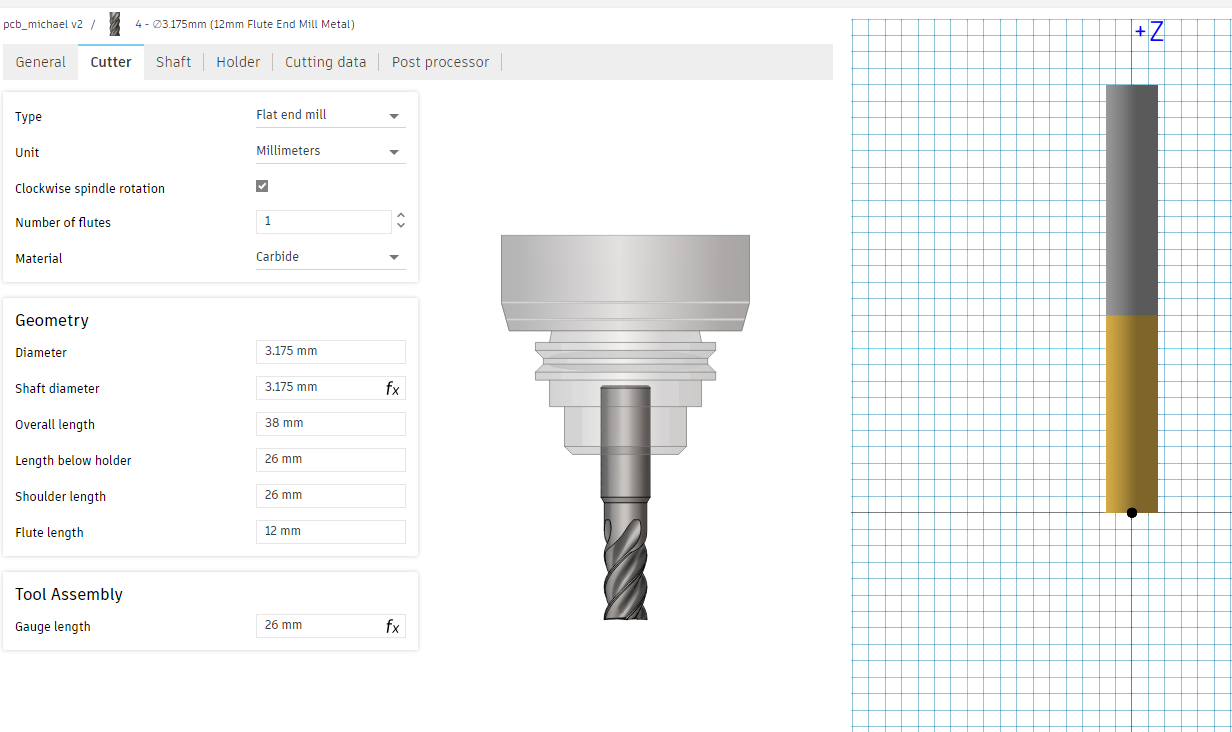
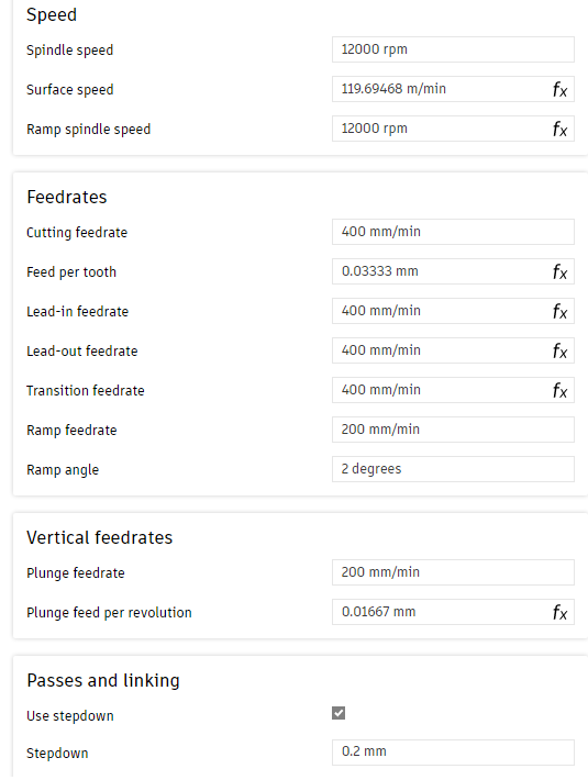
Proper speed and feedrate values are essential to ensure clean cuts, avoid tool breakage, and prolong bit life. Below is a breakdown of the parameters used for PCB engraving in this project:
Screenshot of Fusion 360 CAM settings used for engraving traces on FR1 material.
12000 rpm – Common range for copper engraving:
10000–16000 rpm.
400 mm/min – Horizontal tool movement during material
removal.0.033 mm – Distance advanced per tooth per rotation.400 mm/min – Smooth entry/exit to reduce tool stress.
400 mm/min – Speed when moving between toolpaths.
200 mm/min – Slower speed for gentle entry into material.
2° – Entry angle to avoid vertical plunges.200 mm/min – Vertical descent rate to prevent tool
breakage.0.016 mm – Informative value based on rpm and
feedrate.0.2 mm – Depth removed per layer until final depth is
reached.These cutting parameters were selected based on extensive experience using the Makera Carvera CNC machine at the EAN University's FabLab. The lab routinely offers PCB milling services to students, which has helped establish well-tested and effective machining profiles for FR1 boards. Thanks to this ongoing usage and continuous refinement, we were able to confidently apply settings that ensure clean trace isolation, accurate board outlines, and safe, reliable tool performance.
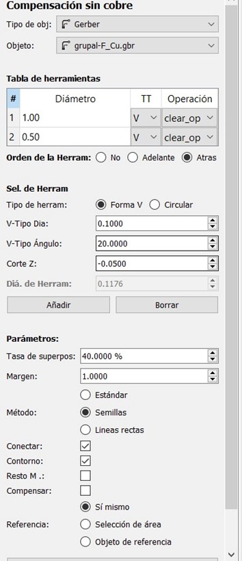
In the Manufacture workspace of Fusion 360, we used the 2D Contour operation to isolate the copper traces on the top layer of the PCB. This strategy allowed precise engraving using the geometry of the PCB design.
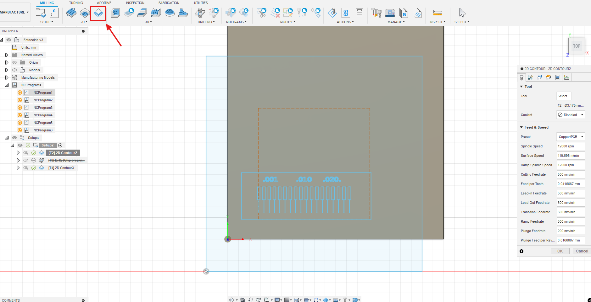
2D Contour operation applied to the top copper layer of the PCB layout.
Configuration highlights:
Speeds, feeds, and cutting depth were inherited from the FabLab EAN standard PCB milling settings, ensuring consistency and reliability across engravings.
The height settings define how the tool approaches and leaves the surface during machining. For PCB trace engraving, the tool must cut just deep enough to remove the copper layer without reaching the substrate.
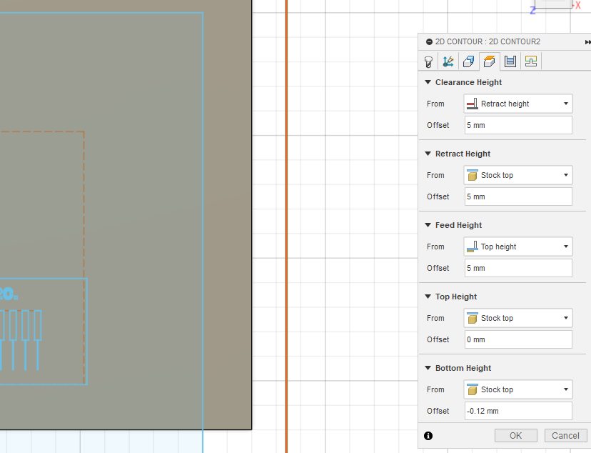
Height settings for 2D Contour operation in Fusion 360.
These values ensure consistent Z-depth across the board surface, especially when combined with the Carvera’s built-in auto-leveling.
For the final stage of the PCB milling process, we created a separate 2D Contour operation specifically for cutting out the board outline. This operation used a different tool and adjusted height parameters to cut through the full thickness of the FR1 substrate.
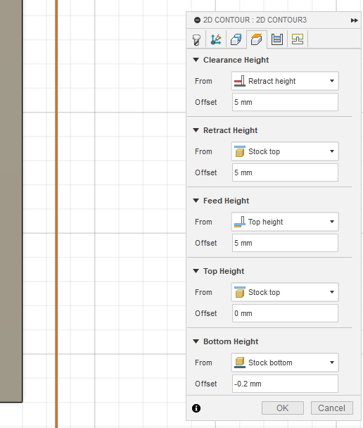
Height settings configured in Fusion 360 for the board outline operation using the Flat End Mill (Flute Bit).
Configuration details:
From Stock bottom – Offset: -0.2 mm – ensures full material
separation with a slight overcut.Using a dedicated operation and the Flat End Mill (Flute Bit) allowed us to perform the final cutout efficiently and without damaging the board. The tool’s geometry and cutting depth were ideal for removing the material in one or two passes, supported by the automatic tool change system of the Makera Carvera.
Once all toolpaths were created and validated, the final step was to generate the machine-readable G-code. For this, we used the Post Process function within the Fusion 360 Manufacture workspace.
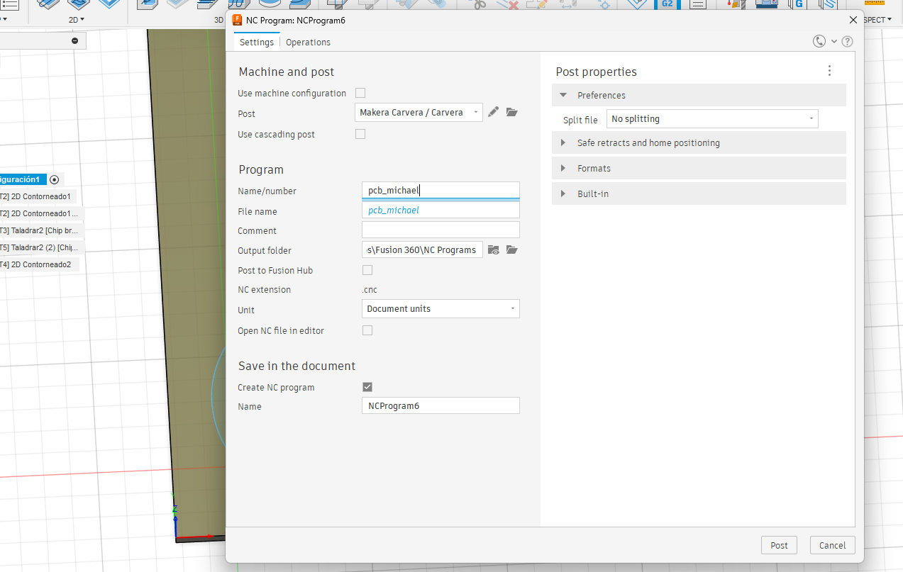
Post-processing configuration using the Makera Carvera-specific post processor.
Steps followed:
pcb_michael..cnc extension, ready for upload to the machine’s control
software.This step ensures that all toolpath operations are correctly translated into G-code instructions that the Carvera understands, including motion control, feedrates, spindle speed, and safe retracts. The post processor handles any formatting or command translation specific to the Makera firmware.
With the G-code exported, we proceeded to set up the Makera Carvera and manufacture the PCB. This process involved mounting the board, uploading the file, calibrating the machine, and supervising the milling.
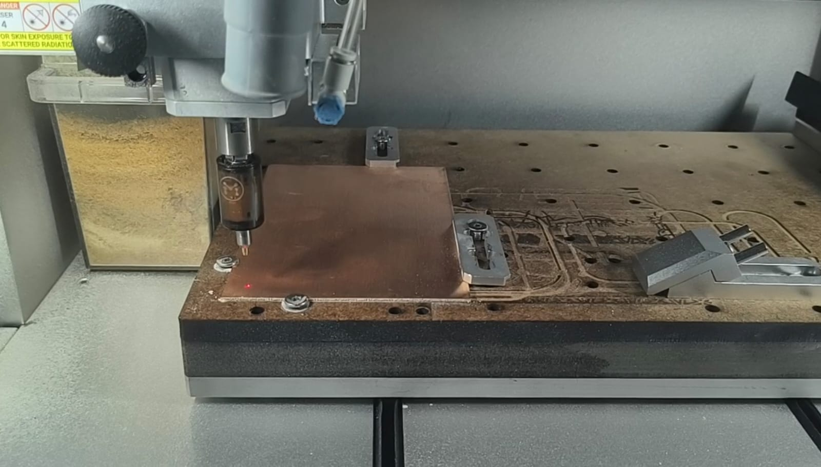
In this image, the Carvera is performing the Z-axis height calibration with the V-bit tool installed.
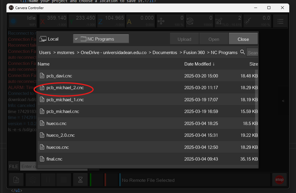
G-code file selection screen showing the uploaded pcb_michael_2.cnc
file.
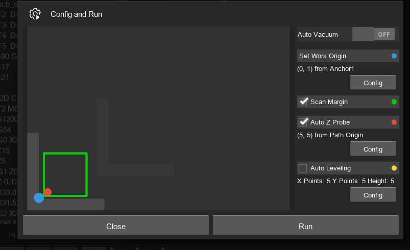
Makera interface for defining work origin, Z probing, and scan margin before milling.
The Makera Carvera's features like smart probing and automatic tool changing made the manufacturing workflow smooth and reliable. Proper fixturing, origin setup, and Z calibration were critical to ensuring accuracy throughout the job.
After completing the manufacturing process with the Makera Carvera, the final test board was carefully inspected under a microscope. Below is a visual summary of the milling process and results.
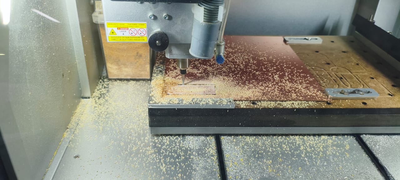
Makera Carvera actively engraving the copper surface to create trace isolation paths.
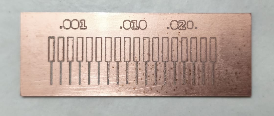
Final result of the milled test board, showing three trace width groups: 0.001", 0.010", and 0.020".
We used a digital microscope to verify the quality, precision, and depth of the engraving. The following images highlight various trace widths:
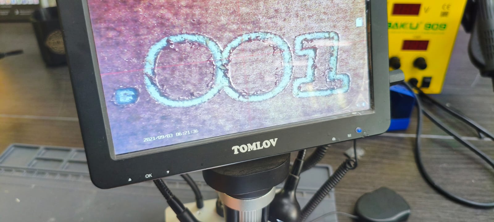
Engraving detail of .001" group under microscope.
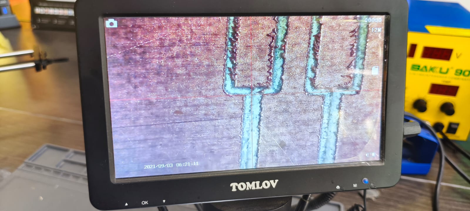
Close-up of a narrow channel showing trace isolation effectiveness.
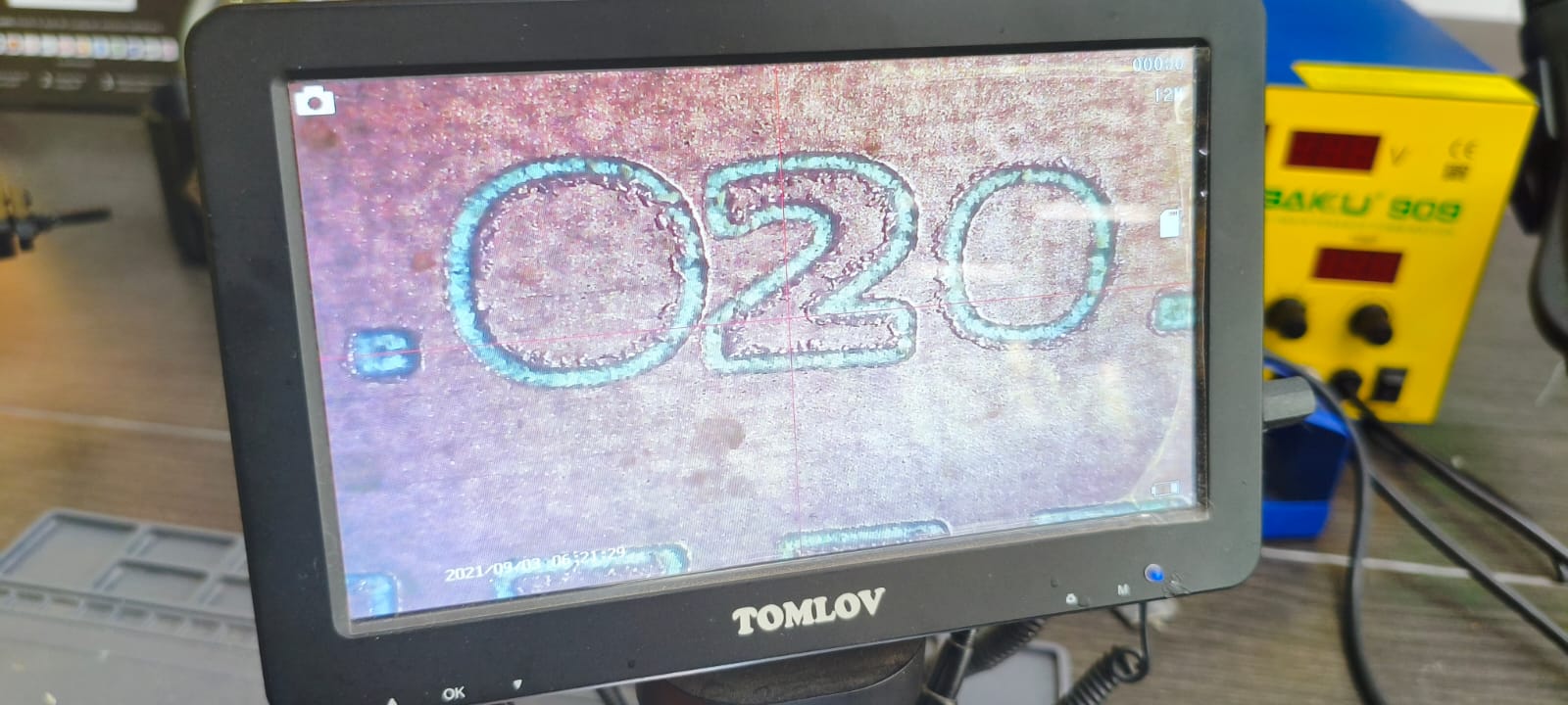
View of the .020" text under the microscope, confirming sharp engraving.
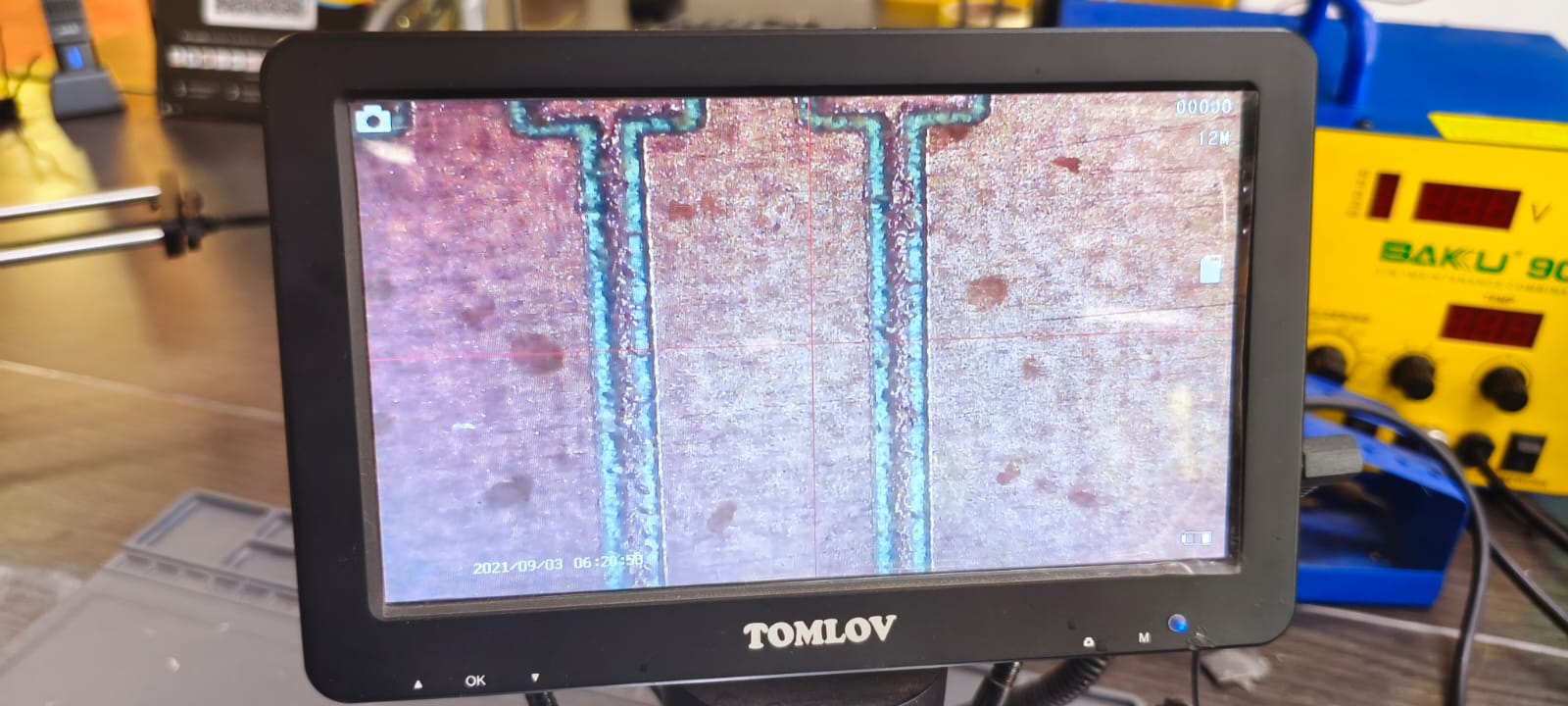
Inspection of wider traces, confirming consistent depth and definition across the board.
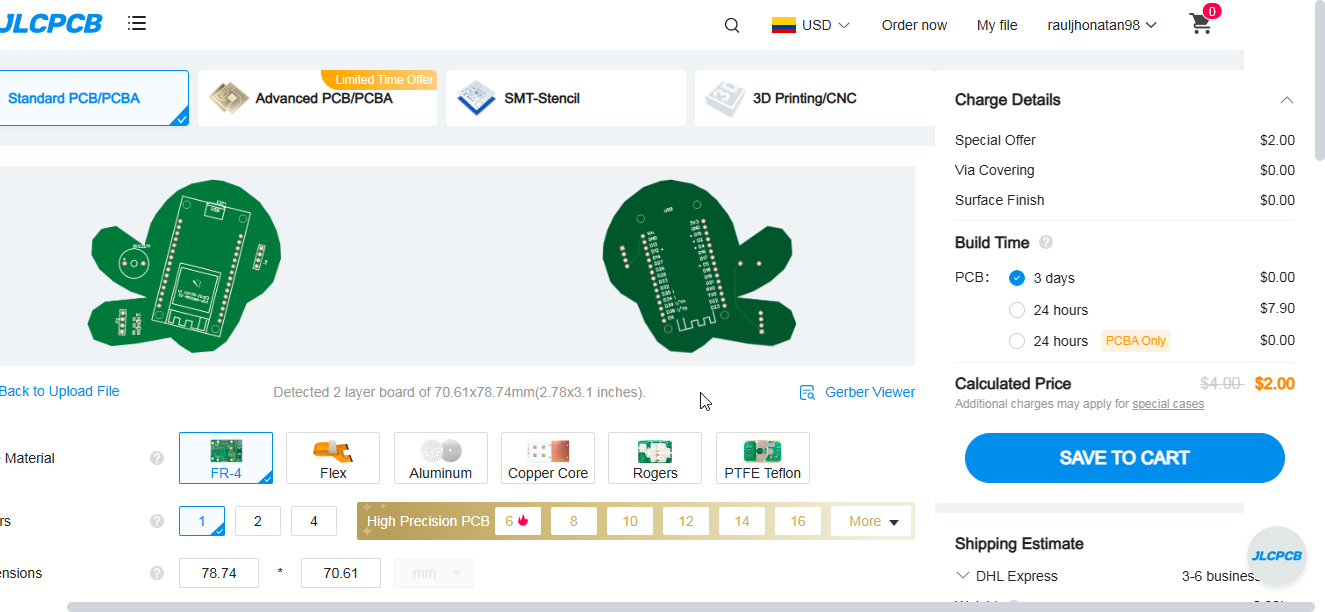
After completing the design of my PCB in EasyEDA, I decided to manufacture it using JLCPCB, one of the most accessible and reliable PCB fabrication services available. Fortunately, EasyEDA integrates directly with JLCPCB, which simplifies the workflow from design to production.

Within EasyEDA, I used the "Fabrication > Order at JLCPCB" option to start the process directly from my design file.

This opened the JLCPCB interface where I could configure all fabrication parameters including board thickness, color, finish and delivery speed.
Before submitting, I reviewed my PCB layout and used the “Export Gerber” function. EasyEDA then opened a DRC check window, followed by an upload panel to submit the Gerber directly to JLCPCB.

Here I confirmed that everything was ready for fabrication and chose to proceed with Gerber upload to JLCPCB.
The platform automatically loaded the design, saving me time and ensuring consistency between the layout and the file to be manufactured.
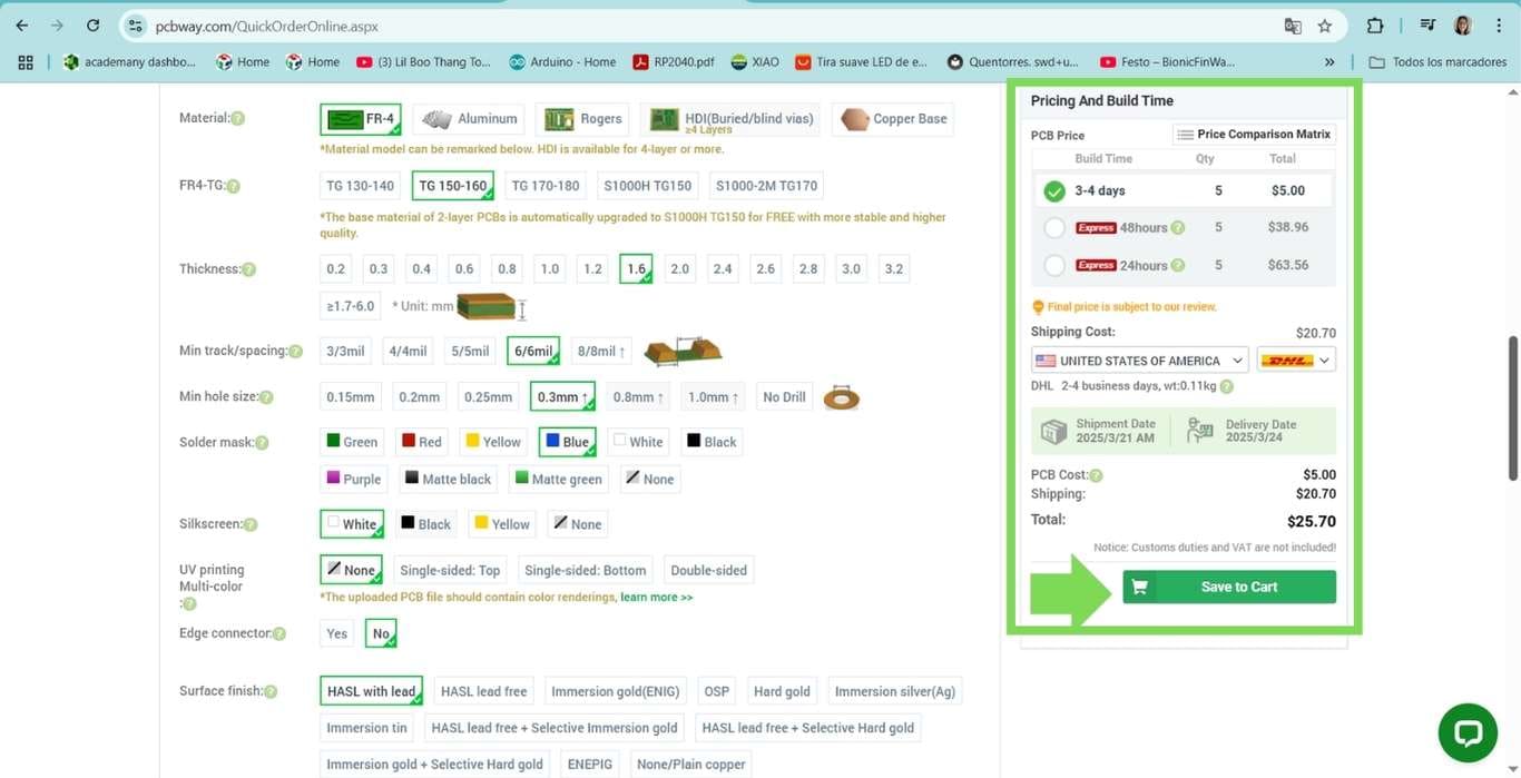
For this board, I configured the following settings: 1.6 mm PCB thickness, green solder mask, white silkscreen, HASL (with lead) surface finish, 1 oz copper weight, and tented vias. I selected a regular outline tolerance of ±0.2 mm and a production time of 2 days.


After confirming all parameters, I proceeded to the cart, where I entered shipping and billing information. The platform allows easy checkout and international delivery, making it possible to receive professional-quality PCBs at an affordable cost.

Final checkout step, where I confirmed country of delivery, quantity, and other order details before placing the order.
This assignment allowed me to deepen my understanding of the full PCB fabrication workflow using CNC technology. I learned how to properly configure cutting parameters in Fusion 360, apply toolpath strategies for both traces and outlines, and export G-code compatible with the Makera Carvera machine.
One of the most valuable aspects was calibrating the Z-axis and understanding how small changes in depth and feedrate significantly affect engraving quality. Observing the microscopic results helped me analyze the precision achieved at different trace widths and reinforced the importance of using the right tool for each job.
Working at the FabLab EAN has been an enriching experience, as it provides access to advanced prototyping equipment and a collaborative space where students can manufacture their own PCBs. I now feel more confident using CNC milling machines for electronic production and look forward to applying this knowledge in future projects.
After analyzing the test results under the microscope, I concluded that the 0.020" trace width offers the best balance between precision, tool durability, and electrical reliability. The engraving is clean, the copper removal is consistent, and there is minimal risk of over-etching or trace breakage during milling. In contrast, the 0.001" width, while visually sharp, tends to produce fragile and narrow paths that can be affected by slight tool or surface variations, making them less reliable for functional circuits. This insight will guide my future designs, especially when considering manufacturability and repeatability in PCB fabrication.
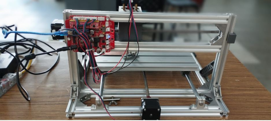
The group project was carried out at the UNCP Fab Lab. We used a small CNC-PBC machine in this lab. Initially, it presented some problems, such as looseness in some of the engine mount bolts. We had to make some adjustments and also install the finest 0.1 mm and 0.2 mm cutters. We then used the CNC milling machine and performed some initial motion tests.
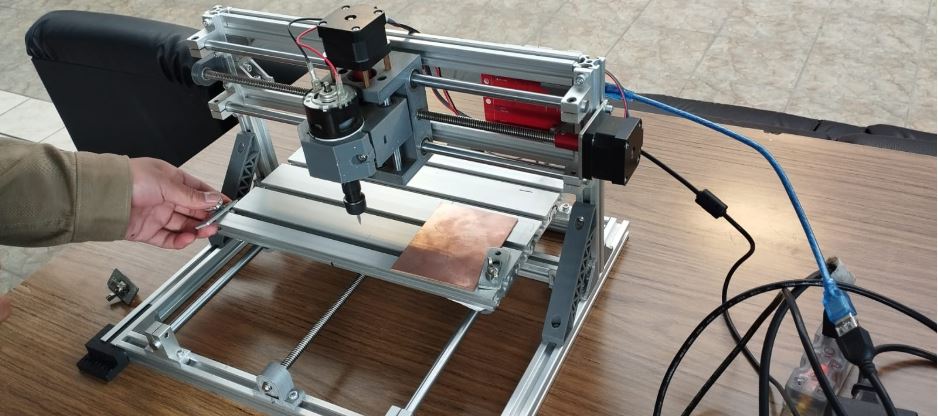
For this work we have used the CNC machine type CNC 2418, which is commonly used for PCB engraving, wood milling, and light router, with a working area of approximately 240 x 180 mm, below are its technical specifications.
| Feature | Specification |
|---|---|
| Machine Type | Desktop CNC Engraving & Milling Machine |
| Work Area (XYZ) | 240 × 180 × 40 mm |
| Axes | 3 (X, Y, Z) |
| Motors | NEMA 17 Stepper Motors |
| Controller | GRBL-based (usually Arduino) |
| Spindle | DC 12–24V, 3000–12000 RPM |
| Precision | ~0.01 – 0.05 mm |
| Max Speed | ~3000 mm/min (depending on setup) |
| Supported Materials | PCB, wood, acrylic, soft plastic |
| Software | UGS, Candle, bCNC |
| Frame Material | Aluminum + ABS components |
Motion testing on CNC PCB (printed circuit board) milling machines is essential to ensure the equipment's accuracy, repeatability, and safety before milling the board. In addition, no-load testing is also essential to verify that the axes move according to the programmed path
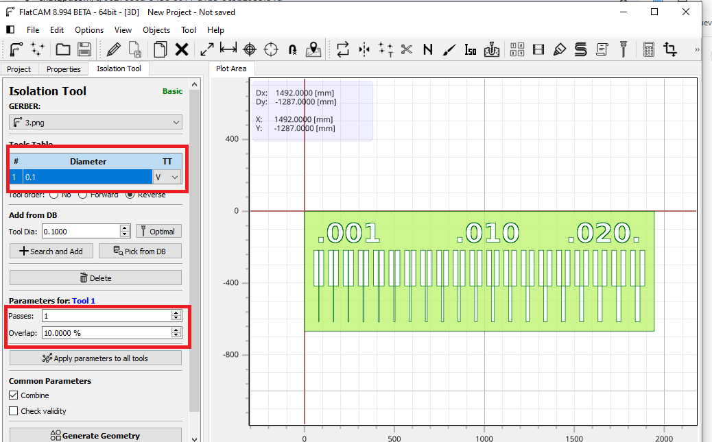
To carry out the tests with the machine, we first download the file from the example provided in class. Then, using the Flatcam software, we import the downloaded image.
PNG image downloaded from the Fab Academy files, once downloaded, we imported the image as an object in Flatcam.
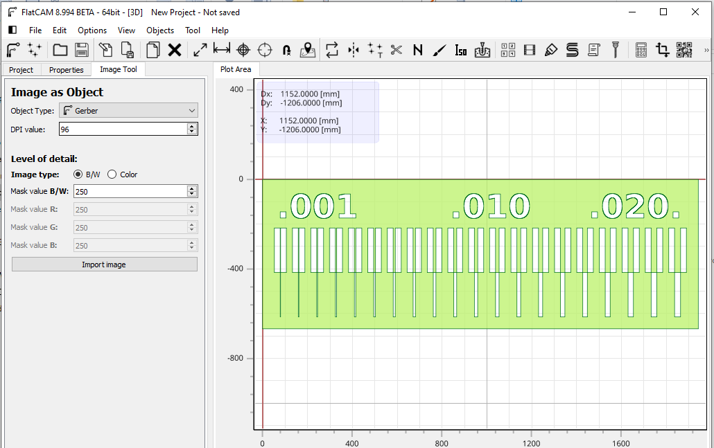
As you can see, the downloaded image was imported successfully. Next, we set up the tool; in this case, we selected a 0.1 mm, 30° V-shaped cutter.
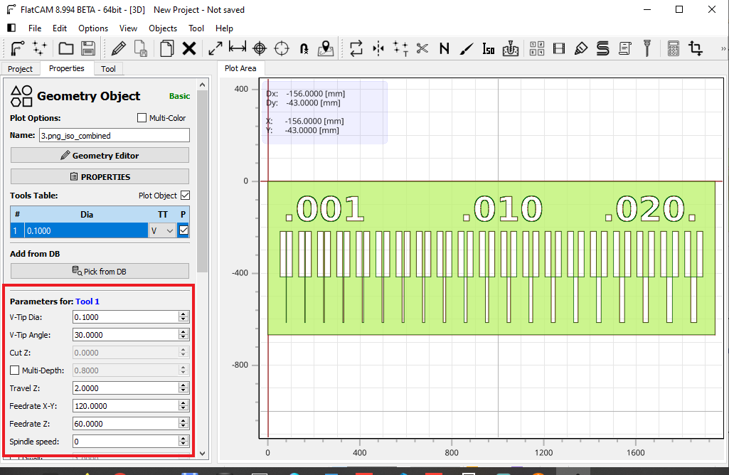
A window will then open where we will set the speed parameters for the XY axes and the lowering and raising speed in Z.
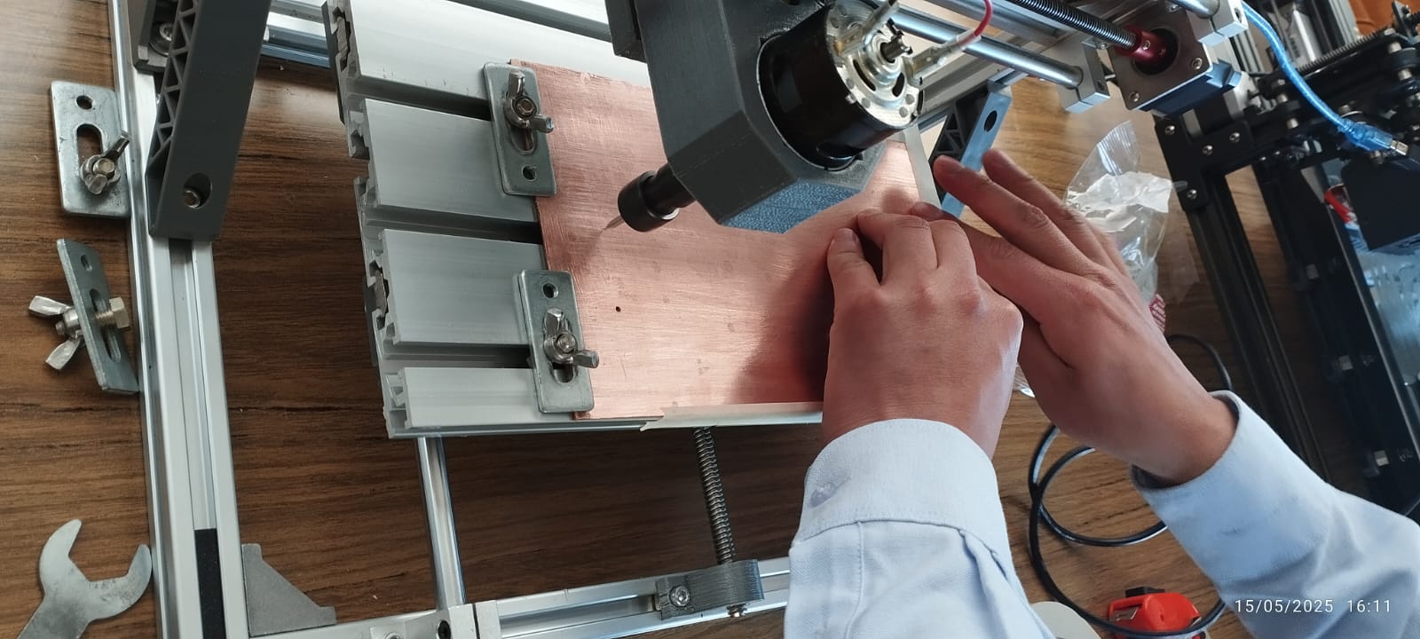
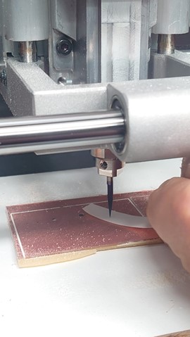
Once the test image design was configured in FlatCAM, I proceeded to fix the Bakelite in the work area. To be able to cut the Bakelite, I used a 0.1 mm cutter with a 30° angle.
Machining process.
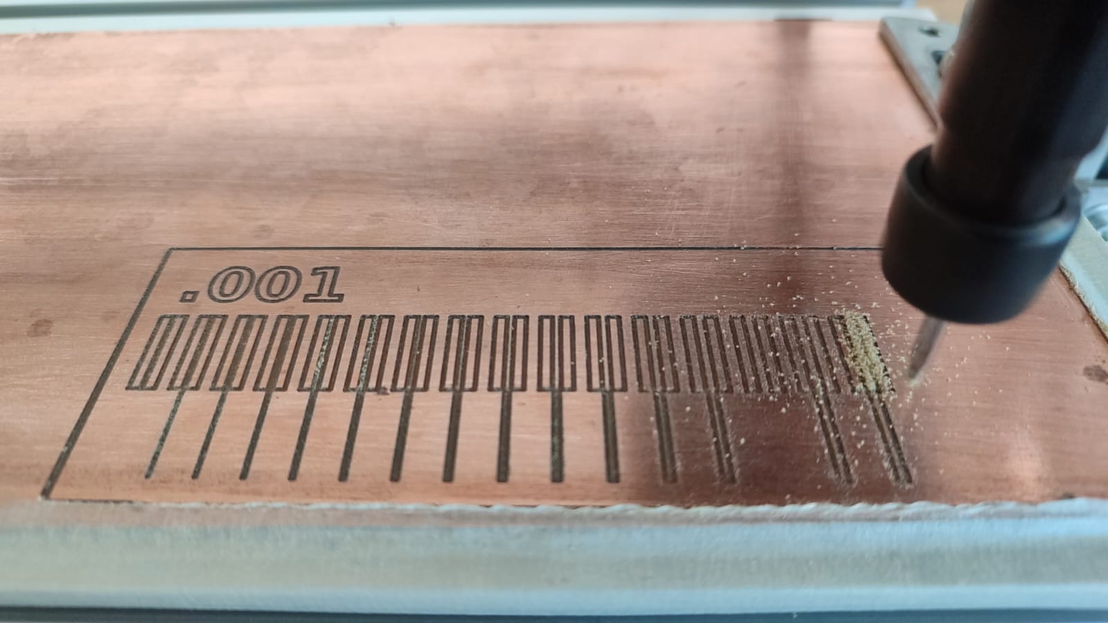
Almost finishing the machining process and we see that the results are satisfactory.
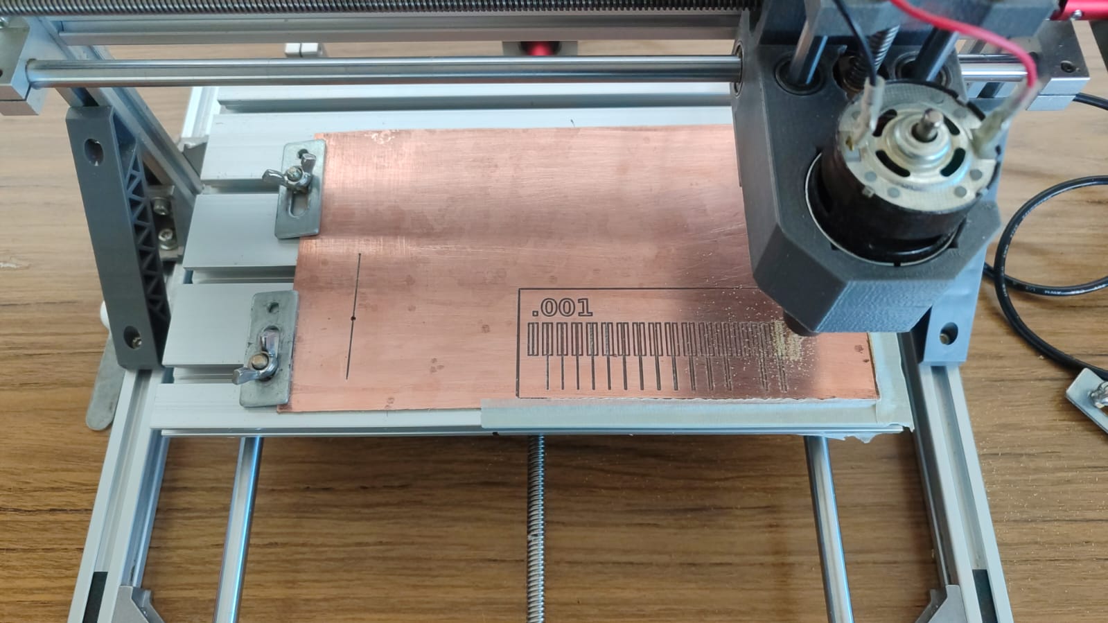
After completing the manufacturing process with the CNC 2418 PCB, the work area was cleaned and the final test board is shown with satisfactory results, with the appropriate adjustments, and the necessary configurations a good result was achieved.
Another way is to send our PCB to be manufactured by companies dedicated to this sector. In this case, look for PCBWay, a Chinese company dedicated to the manufacture of PCBs on a large scale.

To fabricate the board, we first accessed the website PCBWay

After entering the website https://www.pcbway.com, we logged into an existing account (or created a new one if needed). Having an account allows access to features like:

Then we fill in the information they ask for, such as the email address, among others.

After logging in and accessing the main dashboard, we navigated to the "PCB Instant Quote" section and selected the "Standard PCB" option. This category is suitable for most custom PCB prototypes and small production runs.

After selecting the "Standard PCB" option and filling in the basic specifications, we uploaded the Gerber ZIP file containing all the necessary manufacturing files.

PCBWay automatically processed and displayed a preview of the design, allowing us to verify:
If any issues were found in the preview, the design could be corrected and re-uploaded. Once the Gerber files were verified, we proceeded to submit the order.
This report presents our group's collaborative experience in characterizing the process of fabricating printed circuit boards (PCBs) in our lab. We carefully documented key parameters such as feed rates, spindle speeds, depths of cut, and tooling setups, while also reflecting on the workflow from start to finish.
| Parameter | Value |
|---|---|
| Feed Rate (X/Y) | 120 mm/min |
| Plunge Rate (Z) | 60 mm/min |
| Spindle Speed | 10,000 RPM |
| Cut Depth (Traces) | 0.1 mm |
| Cut Depth (Outline) | 0.8 mm |
| Tooling | V-bit (0.4 mm), End mill (1.0 mm) |
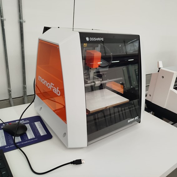
Our team used the Monofab SRM-20 CNC milling machine, known for its precision on FR-4 or phenolic copper-clad boards. It proved ideal for our prototyping needs.
To ensure everything was working properly, we started with a standard test design. This allowed us to verify the basic setup and machine functionality before moving on to custom designs.

We selected specific calibration patterns from the Fab Academy library. These are designed to help verify the accuracy and alignment of the machine across small and detailed geometries.

As a group, we thoroughly reviewed the PCB design in our CAD software to confirm the geometry was correct and error-free before exporting.

We exported the required Gerber files for traces and the accompanying drill files. This step was crucial for preparing the layout for the milling process.

All generated files were saved and organized for easy import into FlatCAM during the toolpath generation stage.

Using FlatCAM, we imported the Gerber and drill files to create toolpaths. This software allowed us to fine-tune machining parameters before generating the final G-code.

We carefully examined the imported files to ensure trace alignment and correct toolpath generation.

Our team opted for V-bit tools (typically 0.4 mm) for the trace isolation milling and a 1 mm flat end mill for the board outline.

We configured the CNC settings as follows: 120 mm/min feed rate, 60 mm/min plunge rate, 0.1 mm depth of cut for traces, 0.8 mm for outline cuts, and spindle speeds ranging from 8000 to 12000 RPM.
FlatCAM generated the final G-code files, which we saved for use in the SRM-20 milling software.

We established the zero point (G54) on the material surface, ensuring alignment before starting the job.

The previously generated G-code was loaded onto the SRM-20 interface, and we confirmed all settings matched our defined parameters.

We carefully adjusted the tool height on the Z-axis using a manual calibration process to ensure the first layer cut through the copper surface cleanly.

The CNC milling process was initiated. Each team member took turns supervising the job, checking for consistent toolpaths and material removal.


The result was a clean, precisely milled PCB with accurate traces and a defined board outline, ready for component soldering.
This project allowed us to collaboratively explore each stage of the PCB fabrication process. From design to milling, we gained hands-on experience in toolpath generation, machine calibration, and file management. We also learned to work as a team, ensuring quality control at every step and troubleshooting minor issues together. The process enhanced our understanding of digital fabrication and PCB prototyping workflows.